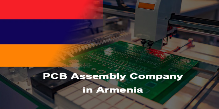
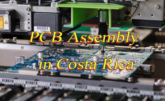
Looking for reliable, fast PCB assembly in Costa Rica? Tired of delayed lead times, inconsistent quality, unstable components, or incomplete turnkey services? EBest is your trusted solution for PCB assembly in Costa Rica and the top pick among PCB assembly companies in Costa Rica. We solve your biggest production headaches with speed, certified quality, and end-to-end support. Read on to see how we power your project success.
Why Choose EBest for PCB Assembly in Costa Rica?
Choosing the right partner for PCB assembly in Costa Rica directly impacts your product quality, lead time, and project success. EBest combines two decades of expertise, industry‑leading certifications, advanced equipment, and end‑to‑end support to deliver consistent, high‑quality results. Here’s why we stand out among PCB assembly companies in Costa Rica.
- 19+ Years of Professional PCB Assembly Experience: We bring proven process stability and technical expertise to every PCB assembly in Costa Rica project, from prototypes to high-volume production. Our long-term experience reduces risks and improves efficiency for your products.
- One‑Stop Full Turnkey PCB Assembly Solutions: We handle everything: PCB fabrication, component sourcing, assembly, testing, and final box build. You save time, simplify management, and avoid coordination issues across multiple suppliers.
- Ultra‑Fast Lead Times & Quick‑Turn Support: Standard lead time is just 1–5 days for PCB assembly in Costa Rica. Urgent orders ship in 24 hours to support your tightest deadlines and speed up time‑to‑market.
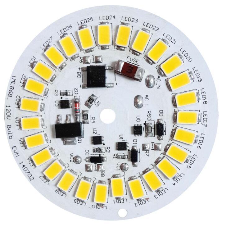
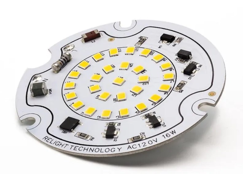
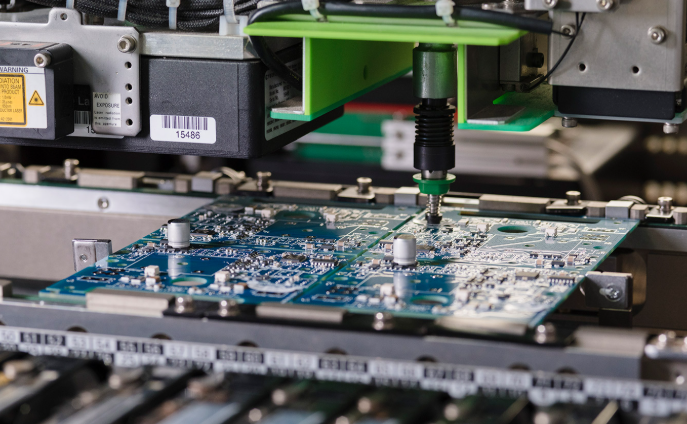
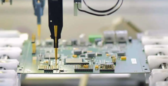
- High‑Precision Assembly Capabilities: We support 01005 micro components and 0.25mm fine‑pitch BGA with full X‑ray inspection. High‑density designs run reliably with zero quality compromise.
- Global Certifications for High‑Rel Industries: IATF 16949, ISO 9001, ISO 13485, AS9100D, RoHS, REACH, UL certified. Your PCB assembly in Costa Rica fully meets medical, aerospace, automotive, and industrial standards.
- Stable & Secure Component Supply Chain: Our global sourcing network ensures reliable delivery of electronic components. We minimize shortages, delays, and obsolescence risks for your production plan.
- 100% Full Inspection Before Shipment: Every board passes AOI, X‑ray, functional testing, and visual inspection. You receive consistent, defect‑free quality for every order.
- Dedicated Customer Support & Custom Solutions: We provide personalized service, clear communication, and flexible processes tailored to your project needs. You get responsive support from quote to delivery.
Common Pain Points in PCB Assembly in Costa Rica & Our Solutions
Pain Point 1: Long and unpredictable lead time.
Our Solution: 1–5 day standard lead time; 24-hour expedite service for urgent orders.
Pain Point 2: Unstable electronic component supply.
Our Solution: Global stable supply chain for SMD, BGA, QFN, QFN, QFP and all parts.
Pain Point 3: Cannot assemble micro-components and fine-pitch BGA.
Our Solution: Support 01005 components and 0.25mm BGA pitch with X-ray inspection.
Pain Point 4: Lack of medical, aerospace, automotive certifications.
Our Solution: IATF 16949, ISO 9001, ISO 13485, AS9100D, RoHS, REACH, UL certified.
Pain Point 5: Inconsistent quality and high defect rates.
Solution: 100% full inspection including AOI, X-ray and functional testing.
Pain Point 6: Fragmented suppliers and complicated management.
Our Solution: One-stop full turnkey PCB assembly solutions.
Pain Point 7: No support for prototypes and small-batch production.
Our Solution: Professional prototype & quick-turn PCB assembly services.
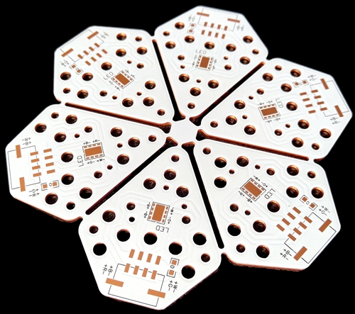
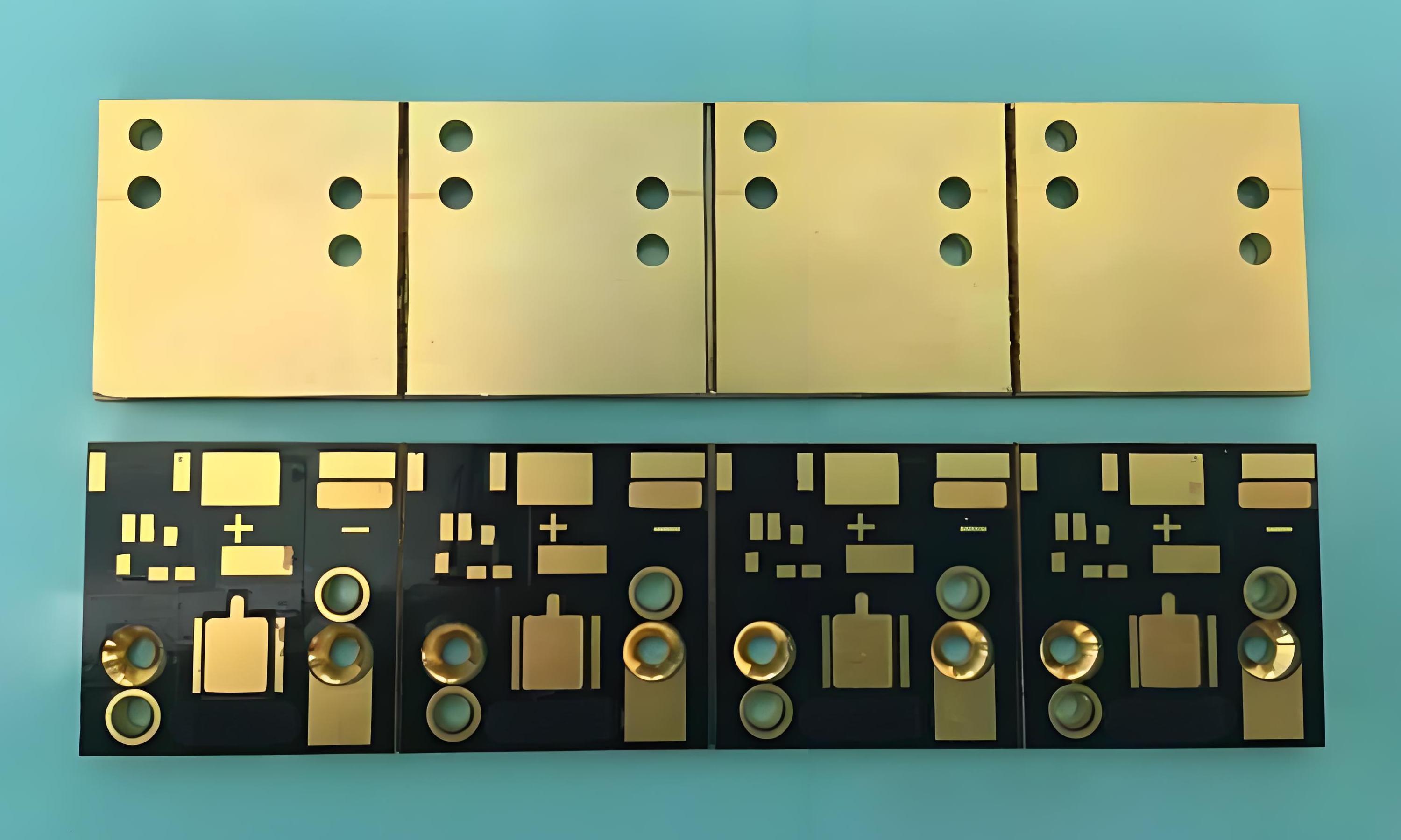
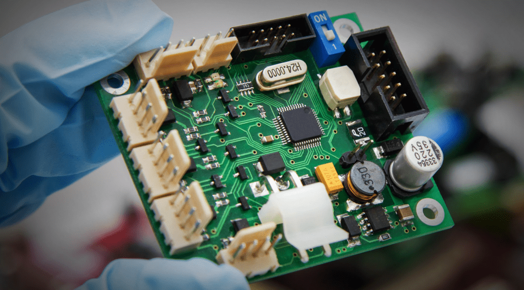
Our Full PCB Assembly Services in Costa Rica
Core Assembly Services
- SMT Assembly
- Through‑Hole (THT) Assembly
- Mixed SMT + THT Assembly
- BGA Assembly
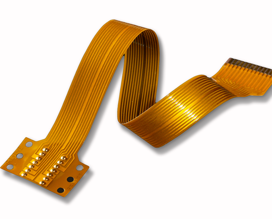
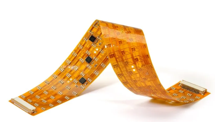
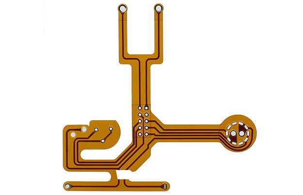
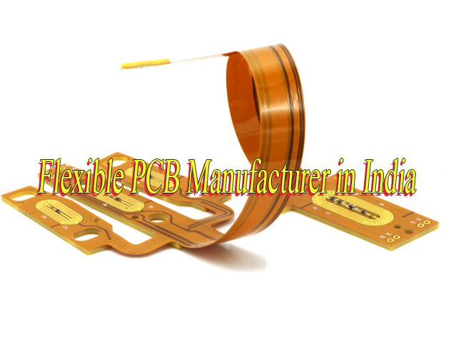
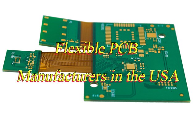
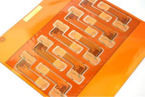
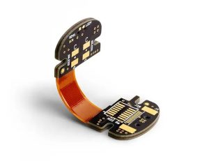
- Flex PCB Assembly
- Ceramic PCB Assembly
- Prototype PCB Assembly
- Quick Turn PCB Assembly
- Full Turnkey PCB Assembly
Value‑Added Services
- Component sourcing
- Box assembly
- Injection molding
- CNC machining
- Sheet metal fabrication
EBest’s Quality Certifications for Reliable PCB Assembly in Costa Rica
EBest maintains global certifications to support regulated PCB assembly in Costa Rica:
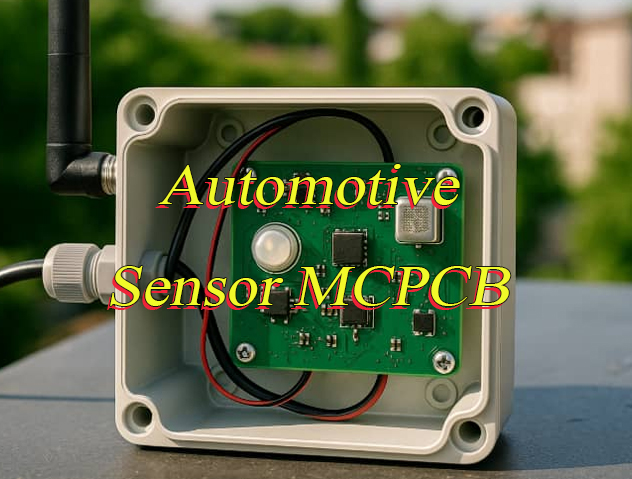
- IATF 16949: Certification for automotive quality management systems.Supports automotive PCB assembly with strict process control and zero-defect targets.
- ISO 9001:2015: Global general quality management system standard. Ensures consistent, repeatable quality across all PCB assembly in Costa Rica orders.
- ISO 13485:2016: Medical device quality management system certification. Essential for medical equipment, patient monitoring, and diagnostic PCBs.
- AS9100D: Aerospace industry quality standard. Supports high‑reliability aerospace PCB assembly for extreme environments.
- RoHS & REACH: Environmental and substance restriction compliance. Ensures products meet EU and international environmental requirements.
- UL: Safety certification for electronic products. Validates safety performance for commercial and industrial electronics.
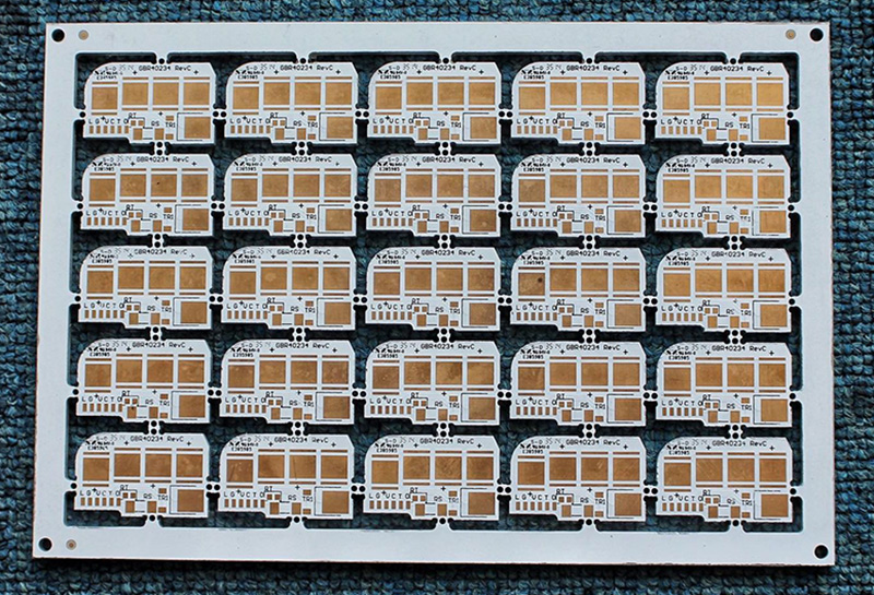
EBest’s Technical Capabilities for PCB Assembly in Costa Rica
| Item | Specification |
| Placement Speed | 13,200,000 chips/day |
| Bare Board Size | 0.2×0.2 in – 20×20 in / 22×47.5 in |
| Minimum SMD | 01005 |
| Minimum BGA Pitch | 0.25mm |
| Max Component Area | 50×150mm |
| Assembly Type | SMT, THT, Mixed |
| Component Package | Reel, Cut Tape, Tube, Tray, Loose Parts |
| Lead Time | 1–5 days |
How Fast Is PCB Assembly in Costa Rica with EBest?
At EBest, we optimize sourcing, production, and inspection workflows to deliver industry‑leading lead times without compromising quality. We support both standard orders and urgent requests to match your project timeline.
- Standard lead time: 1–5 business days for most PCB assembly in Costa Rica orders.
- Expedited service: 24‑hour turnaround for emergency prototype and production boards.
- Parallel processing: Component sourcing, PCB fabrication, and assembly run at the same time to cut total lead time.
- Quick‑turn lines: Dedicated production lines for prototypes and small batches to avoid delays.
- Stable logistics: Efficient order handling and shipping coordination for on‑time delivery to Costa Rica.
Whether you need rapid prototyping, small‑batch production, or urgent mass assembly, EBest ensures your PCB assembly in Costa Rica is completed and shipped as fast as you need.
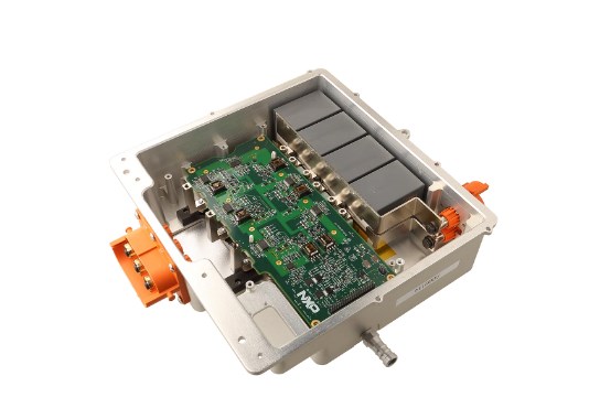
Medical & Aerospace & Industrial PCB Assembly Cases
We have rich experience in PCB assembly in Costa Rica for high‑reliability industries, with certified processes to meet strict performance and compliance demands.
For medical device PCB assembly, we operate under ISO 13485 standards with full ESD protection, complete traceability, and strict quality controls. Our assemblies are widely used in patient monitoring, diagnostic equipment, and portable medical devices, ensuring stable and safe operation in clinical environments.
For aerospace PCB assembly, we follow AS9100D requirements to deliver highly robust boards engineered for extreme temperatures, vibration, and harsh conditions. Every board undergoes rigorous inspection and testing to meet the high‑reliability demands of aviation and aerospace systems.
For industrial equipment PCB assembly, we focus on durability, long lifecycle, and stable performance under continuous operation. Our high‑density assembly and strong anti‑interference design support industrial controls, automation systems, and heavy‑duty electronic equipment.
All these projects confirm our ability to provide professional, compliant, and stable PCB assembly in Costa Rica for the most demanding industry applications.
Quality Control for PCB Assembly in Costa Rica
Here are our quality control for PCB assembly in Costa Rica:
- Incoming material inspection for PCBs, components, and accessories.
- SMT line monitoring and real-time process control.
- AOI automated optical inspection for fast and accurate defect detection.
- X-ray inspection for BGA, QFN, and hidden solder joints.
- Functional testing to verify electrical performance.
- 100% full inspection before shipment.
- Complete production traceability for all batches.
Prototype & Quick-Turn PCB Assembly in Costa Rica
We specialize in fast, reliable prototype and quick-turn services to speed up your R&D and product launch.
- Support 1-piece to small-batch prototype orders.
- Fast 1–5 day lead time, with 24-hour expedite options.
- High-precision assembly for 01005 components and 0.25mm BGA.
- Consistent process matching mass production.
- Professional testing to validate design and function.
- Flexible order adjustments for R&D needs.
- Quick response for engineering and technical questions.
Full Turnkey Solutions for PCB Assembly in Costa Rica
Our one-stop full turnkey model simplifies your supply chain and reduces management workload.
- Complete PCB fabrication based on your design files.
- Stable global component sourcing for all device types.
- Full SMT, THT, and mixed assembly processes.
- Precision injection molding, CNC, and sheet metal support.
- Box assembly and final product integration.
- Full testing, inspection, and quality certification.
- Single-point contact for order tracking and support.
- On-time delivery to meet your project schedule.
FAQ About PCB Assembly & Manufacturing in Costa Rica
Q1: Do you support prototype and mass PCB assembly in Costa Rica?
A1: Yes, we support both prototype and volume production.
Q2: What is the smallest component you can assemble?
A2: We reliably assemble 01005 chip components.
Q3: Can you process fine‑pitch BGA?
A3: Yes, we support 0.25mm BGA pitch with X‑ray inspection.
Q4: How long is standard lead time?
A4: 1–5 days; urgent orders in 24 hours.
Q5: Do you provide full turnkey PCB assembly?
A5: Yes, we manage PCB fabrication, components, and full assembly.
Q6: Is 100% inspection included before shipping?
A6: Yes, every order is fully inspected before delivery.
Q7: Can you support medical, aerospace, and industrial projects?
A7: Yes, with certified processes and strict quality controls.
Contact EBest for Your PCB Assembly in Costa Rica Project
Tired of delayed lead times, inconsistent quality, unstable components, or incomplete turnkey services for PCB assembly in Costa Rica? Stop letting production headaches slow down your project. EBest delivers fast, certified, high‑precision PCB assembly in Costa Rica with full turnkey solutions and 100% inspection. Ready to start your project with a reliable partner? Send us your files and requirements to place your order today: sales@bestpcbs.com.