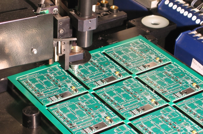
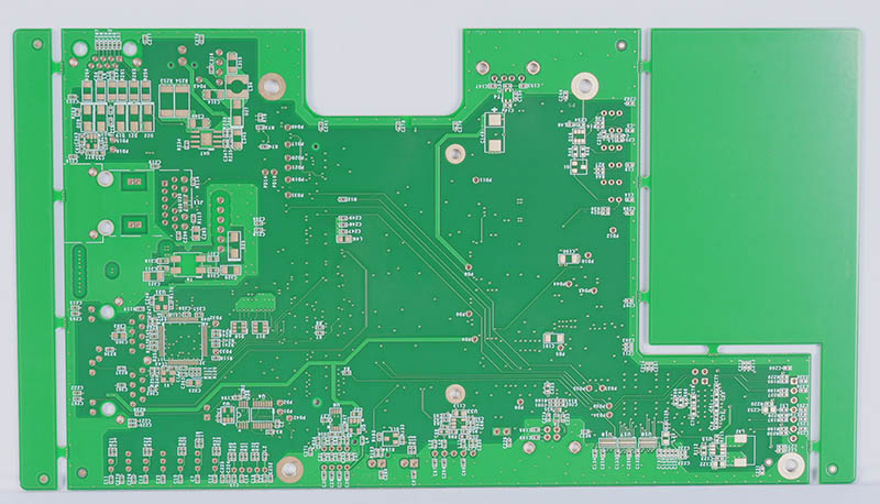
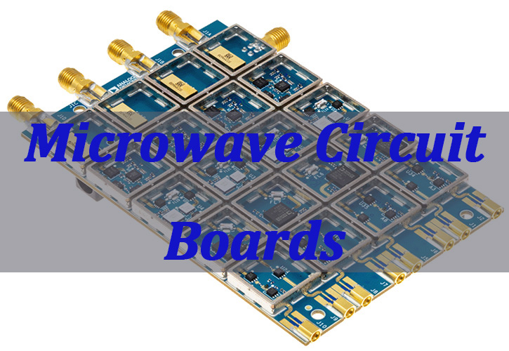
Microwave circuit boards are the specialized backbone of modern high-frequency electronics, enabling the transmission and processing of signals in the GHz to tens of GHz range. This article delves into the design, manufacturing, and material intricacies of these critical components, providing a comprehensive guide for engineers and procurement specialists navigating the RF and microwave PCB landscape.
Developing a successful high-frequency product is fraught with challenges. What Are Key Performance Challenges in RF and Microwave Printed Circuit Boards for Multi-GHz Systems?
- Signal Degradation & Loss: Excessive insertion loss and poor signal integrity at target frequencies, rendering the system inefficient or non-functional.
- Impedance Mismatch & Reflections: Inconsistent dielectric constants and imprecise trace geometries causing signal reflections, standing waves, and degraded power transfer.
- Thermal Management Failures: Inadequate material selection or design leading to overheating, delamination, and permanent performance drift in active circuits.
- Prototype-to-Production Inconsistency: Performance metrics that are achievable in the lab but cannot be reliably replicated in volume manufacturing due to process variability.
- Cost and Timeline Overruns: Unforeseen manufacturing complexities, material waste, and multiple prototype spins that blow budgets and miss critical market windows.
Overcoming these hurdles requires a manufacturer with deep domain expertise and a holistic approach. A premier microwave circuit board manufacturer like BEST Technology addresses these core issues directly.
- Advanced Material & Process Mastery: Utilizing low-loss, thermally stable substrates and controlled processes to minimize Df and ensure consistent Er, directly combating signal loss.
- Precision Engineering & DFM: Implementing strict impedance control with tight tolerances on trace width, spacing, and copper profile to eliminate mismatches and reflections.
- Integrated Thermal Design Support: Recommending and processing materials with optimal thermal conductivity and designing for efficient heat dissipation from the outset.
- Design for Manufacturing (DFM) Review: Providing expert, early-stage DFM analysis to ensure designs are not only functional but also manufacturable and scalable with high yield.
- Streamlined Turnkey Project Management: Offering a complete microwave circuit board factory service—from material procurement to assembly—under one roof, ensuring control, faster turnaround, and predictable costing.
BEST Technology is a premier China microwave circuit board manufacturer specializing in high-frequency, high-reliability PCBs. Our expertise lies in delivering full turnkey solutions for complex RF and microwave projects, combining state-of-the-art manufacturing with rigorous testing to ensure your designs perform as intended, from prototype to volume production. For your next project, pls feel free to contact us at sales@bestpcbs.com.
What Are Microwave Circuit Boards?
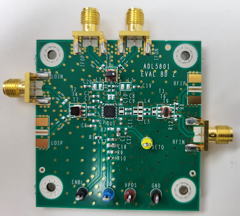
Microwave circuit boards, often referred to as RF and microwave printed circuit boards, are a specialized class of PCBs designed to operate at frequencies typically ranging from about 300 MHz up to 100 GHz and beyond.
Unlike standard digital boards, their primary function is to guide, manipulate, and process electromagnetic waves with minimal loss and distortion. Their performance is critically dependent on the board’s material properties and physical geometry.
How Does Microwave Circuit Board Design Differ From Standard RF and Digital PCB Layouts?
Microwave PCB design transitions from considering signals as simple voltage changes to managing them as electromagnetic waves traveling across a transmission line. This paradigm shift introduces several critical design disciplines not found in lower-frequency layouts. The focus moves from mere connectivity to controlling the electromagnetic field itself.
- Transmission Line Theory is Paramount: Every trace is a controlled-impedance transmission line (microstrip, stripline, coplanar waveguide). Its dimensions must be meticulously calculated based on the substrate’s dielectric constant (Dk) at the target frequency.
- Parasitics Are Performance-Killers: Stray inductance and capacitance from vias, bends, and component pads can no longer be ignored. They must be modeled, minimized, or incorporated into the design as functional elements.
- Material Properties Dictate Design: The dielectric constant (Dk) and its consistency, as well as the dissipation factor (Df), are first-order design inputs, not afterthoughts. Design starts with material selection.
- EM Simulation is Non-Optional: Extensive 3D electromagnetic field simulation is required to predict and optimize S-parameters (e.g., S11 for return loss, S21 for insertion loss) before fabrication.
- Grounding and Shielding are Critical: Preventing radiation loss, crosstalk, and mode conversion requires continuous, low-inductance ground planes and thoughtful cavity isolation.
In essence, microwave circuit board design is an exercise in electromagnetic integrity, where the interplay between physics, materials, and geometry determines success or failure.
Why Manufacturing Precision Matters When Working With Microwave Printed Circuit Boards?
At microwave frequencies, the wavelength of the signal becomes comparable to the physical dimensions of the PCB features. Minor manufacturing variances that are negligible at lower frequencies can cause catastrophic performance shifts. Precision is not a luxury; it is the foundation of functionality.
- Impedance Control: A ±10% variation in trace width or dielectric thickness can lead to a significant impedance mismatch, causing reflections (high VSWR) and reducing power delivered to the load.
- Surface Roughness: Excessive copper foil roughness increases conductor loss, as the signal propagation concentrates near the conductor surface (skin effect). Smoother copper is essential for low-loss performance.
- Dielectric Constant (Dk) Tolerance: Inconsistent Dk across a panel or from batch to batch alters the electrical length and phase of signals, ruining the performance of filters, phase arrays, and couplers.
- Registration and Alignment: Misalignment between layers in multilayer boards changes the effective geometry of controlled impedance lines and can short or couple unintended elements.
| Manufacturing Variance | Potential Impact at Microwave Frequencies |
|---|---|
| Trace Width Tolerance ±15% | Impedance deviation, degraded return loss (S11) |
| Dielectric Thickness Variation | Changed phase & impedance, filter frequency shift |
| Poor Etch Profile (Trapezoidal) | Increased loss, impedance inaccuracy |
| Laminate Dk Tolerance ±0.5 | Shift in electrical length, disrupted timing/phase |
Therefore, partnering with a microwave printed circuit boards factory in China like BEST Technology, which maintains tight process controls, is crucial for predictable, high-performance outcomes.
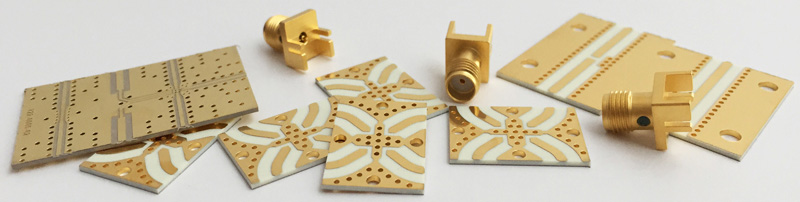
Which Microwave Circuit Board Material Options Support Stable Performance at GHz Frequencies?
The choice of substrate material is the first and most critical decision in microwave printed circuit board design. Ideal materials provide stable electrical properties, low loss, and consistent manufacturability across the required frequency and temperature range.
- PTFE-Based Laminates (e.g., Rogers RO4000® Series, Taconic RF-35): The industry standard for high-performance. They offer extremely low dissipation loss (low Df), stable Dk over frequency/temperature, and low moisture absorption. Ideal for critical circuits like antennas and filters.
- Hydrocarbon Ceramic Filled (e.g., Rogers RO3000® Series): Excellent electrical performance with a lower cost profile than pure PTFE. They provide good thermal conductivity for heat dissipation and are suitable for a wide range of applications.
- Polyphenylene Oxide (PPO)-Based Materials: Offer a balance of performance and cost, with stable Dk and lower loss than standard FR-4, often used in automotive radar and telecom infrastructure.
- Standard FR-4: Not recommended for core microwave functions above 1-2 GHz due to its high and variable Df, inconsistent Dk, and significant loss tangent. It may be used in mixed-signal boards for the digital sections only.
How Are Microwave Circuit Boards Used in High-Frequency Applications?
Microwave circuit boards are enabling technologies across industries that demand high-speed wireless communication, sensing, and data processing.
- Aerospace & Defense: Phased array radars, electronic warfare (EW) systems, satellite communication (SATCOM) terminals, and missile guidance systems.
- Telecommunications: 5G/6G base station antennas and power amplifiers, microwave backhaul links, and millimeter-wave equipment.
- Automotive: Advanced Driver-Assistance Systems (ADAS), including radar sensors (77 GHz) for collision avoidance and adaptive cruise control.
- Medical & Scientific: MRI systems, radiation therapy equipment, and high-frequency test & measurement instrumentation like network analyzers.
Cost Factors That Influence Microwave Circuit Board Price From Prototype to Volume Production
The microwave circuit board price is influenced by several key factors beyond standard PCB costing.
- Substrate Material: Specialty microwave laminates (e.g., Rogers, Taconic) are significantly more expensive than FR-4.
- Layer Count and Complexity: More layers and hybrid constructions (mixing different materials) add cost and processing difficulty.
- Tolerances and Feature Size: Tighter impedance control, finer lines/spaces, and smaller via sizes require advanced equipment and processes, increasing cost.
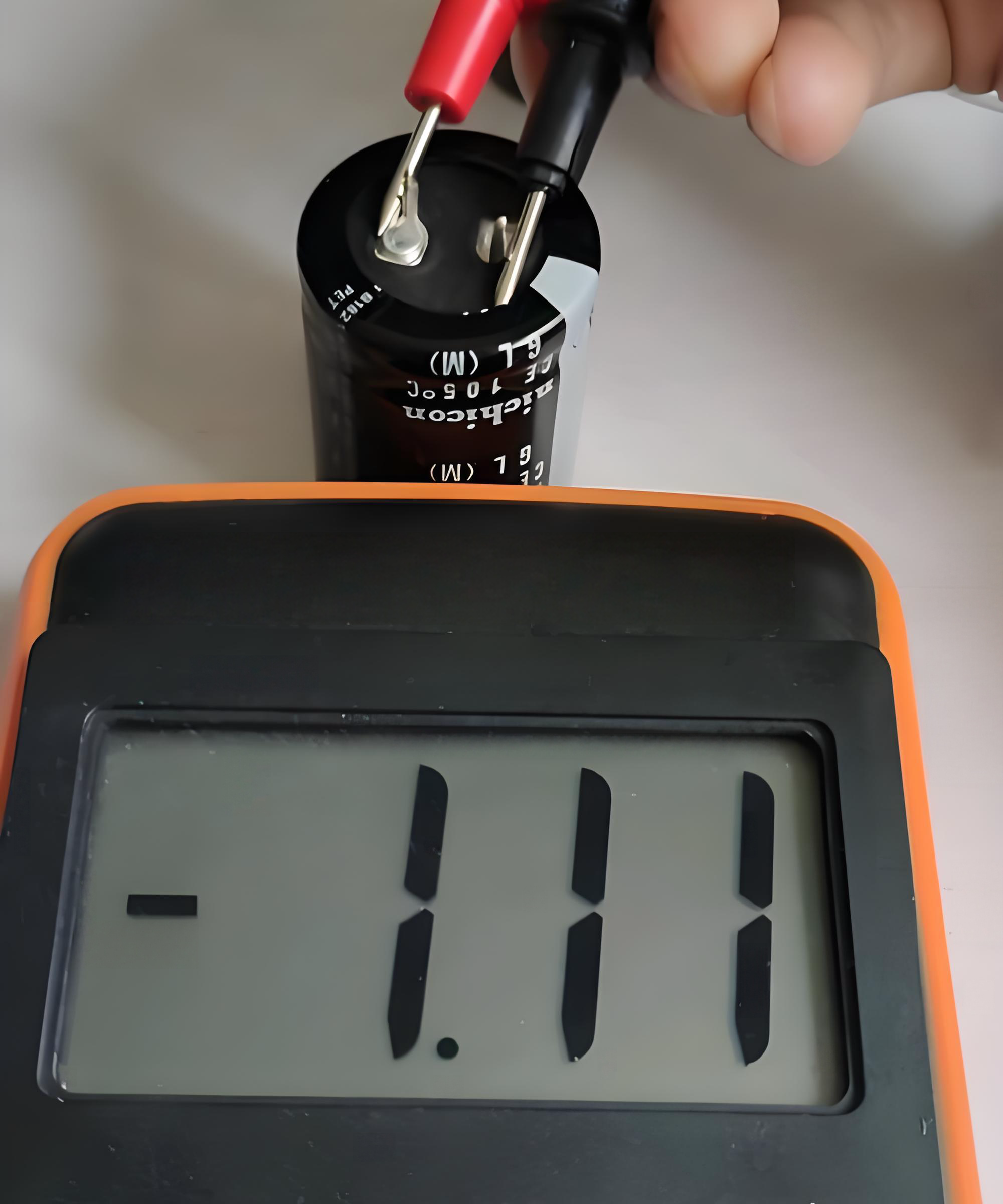
- Testing and Certification: Extensive RF testing (e.g., net analyzer testing), impedance testing, and industry-specific certifications (e.g., ISO, AS9100) add to the cost but are essential for quality assurance.
- Order Volume: Unit cost decreases with higher volumes due to amortized setup and tooling costs, but material cost remains a dominant factor.
How to Select Reliable Best HDI PCB Manufacturers for RF and Microwave Circuit Boards?
Choosing the right partner is critical. Look for manufacturers that demonstrate proven expertise, not just capability. The best HDI PCB manufacturers for RF and microwave circuit boards will exhibit the following:
- Proven High-Frequency Portfolio: Request and review case studies or sample reports of previous work in your target frequency band.
- Material Expertise & Partnerships: They should have deep knowledge of and reliable supply chains for premium laminate suppliers.
- Advanced Process Controls: Inquire about their controls for impedance, etch compensation, lamination, and plating specifically for RF boards.
- In-House RF Testing Capability: The ability to perform basic S-parameter or impedance testing in-house is a strong indicator of serious commitment to the RF market.
- Engineering Support: They should offer proactive microwave circuit board design review (DFM) to catch issues before fabrication begins.
Why is EBest Circuit (Best Technology) Considered a Premier Microwave Circuit Board Manufacturer for Complex RF Projects?
EBest Circuit (Best Technology) has solidified its reputation as a leading microwave and RF circuit board manufacturer by combining nearly two decades of specialized experience with robust manufacturing capabilities and an unwavering commitment to quality.
1. Proven Experience and Scale:
- 19 Years of Focused Expertise: Founded in 2006, we possess 19 years of deep industry knowledge in advanced PCB manufacturing, specifically catering to the demands of high-frequency applications.
- Significant Production Capacity: Our factory boasts a monthly production capability of 260,000 square feet (28,900 square meters), handling over 1,000 different boards monthly. This scale ensures we can manage both prototype and mass production needs reliably.
- Global Client Trust: We have successfully served 1,700+ satisfied clients across 40+ countries, demonstrating our ability to meet international standards and project requirements.
2. Specialized Material and Manufacturing Capabilities for RF/Microwave:
Our technical specifications, as detailed in our capability charts, are precisely aligned with the needs of RF and microwave boards:
- High-Frequency Materials: We are highly experienced in processing specialized laminates critical for RF performance, including Rogers (4003, 4350, 5880), Taconic, and Isola high-speed materials (e.g., FR408HR). We also offer high-Tg FR4 (up to TG >180) for demanding applications.
- Precision Engineering: We achieve fine lines and spaces down to 3/3 mil (0.075/0.075mm) for standard processes and 2/2 mil (0.05/0.05mm) for HDI, which is essential for controlling impedance in high-frequency designs.
- Advanced Layer and Thickness Control: We manufacture multi-layer boards up to 32 layers, accommodating complex RF circuit architectures with controlled impedance tolerances of ±10% (>50 ohm) or ±5 ohm (≤50 ohm).
3. Certified Quality Assurance and Rigorous Testing:
Quality is non-negotiable in RF projects. Our commitment is validated by:
- International Certifications: We hold ISO9001:2015 for quality management and IATF 16949:2016 for automotive quality, underscoring our process discipline. Additionally, we are ISO 13485:2016 certified for medical devices and compliant with RoHS and REACH environmental standards.
- Comprehensive Testing Regime: Our facility is equipped with advanced test equipment like Automatic Optical Inspection (AOI), X-Ray copper thickness testers, Flying Probe Testers, and Micro-section Analysis systems to ensure every board meets stringent quality criteria for signal integrity and reliability.
4. Full Turnkey Solution with Unmatched Speed and Support:
We simplify the supply chain for our clients, providing a seamless journey from concept to final product.
- True One-Stop Service: Our services encompass PCB design, fabrication, component sourcing, PCB assembly (SMT & THT), and full box-build integration.
- Rapid Prototyping: We understand the iterative nature of RF design. We offer expedited services, with urgent FR4 prototypes (1-8 layers) shipping in as fast as 24 to 72 hours.
- Reliable Delivery: We maintain an On-Time Delivery rate of 97%, ensuring your project timelines are met without compromise.
By integrating deep technical expertise, transparent and verifiable capabilities, and a quality-centric culture, EBest Circuit (Best Technology) provides the essential foundation for success in complex microwave and RF projects. We don’t just make boards; we deliver reliable, high-performance solutions backed by data and decades of experience.
To wrap up, microwave circuit boards are the critical, high-performance platforms that make advanced wireless and sensing technologies possible. This guide has explored their unique design requirements, material science, manufacturing imperatives, and application landscapes. BEST Technology stands ready as your full-service partner, offering the material knowledge, precision engineering, and manufacturing excellence needed to bring your most ambitious RF and microwave projects to life with speed. For more information or if you would like to send us any inquiry, please send us an email through the contact form at the bottom of our Contact Page.