Wireless module PCB is a crucial component in modern electronics, enabling seamless communication between devices without the need for physical connections. From smart home systems to agriculture and IoT applications, these PCBs are the backbone of wireless technologies that drive innovation. In the agriculture sector, for instance, wireless module PCBs are enhancing livestock management through solutions like multisensory bands for poultry, providing real-time data to improve productivity and animal welfare. In this blog, we’ll explore how wireless module PCBs work, their applications, and how they are shaping the future of industries like agriculture, IoT, and beyond.
What is a Wireless Module?
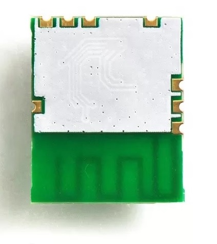
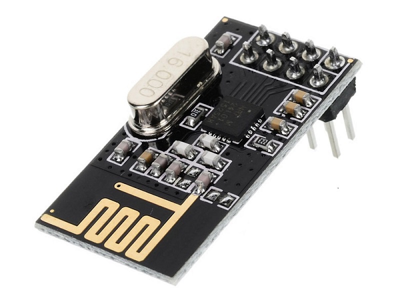
A wireless module is a vital component that allows devices to communicate without physical connections. These modules handle the transmission and reception of wireless signals, making them integral to modern wireless communication systems. They enable IoT (Internet of Things) devices to send and receive data seamlessly, opening the door to smart technologies across various industries.
The key functionality of a wireless module is its ability to handle protocols such as Wi-Fi, Bluetooth, or Zigbee, ensuring data can travel over short or long distances. This communication allows smart devices, like sensors and controllers, to operate in real-time without being tethered to a central hub.
In agriculture, for example, wireless modules provide the backbone for systems like multisensory bands for poultry, where devices transmit critical data about the health and behavior of animals. These modules connect different devices, creating a cohesive network that drives efficiency and innovation.
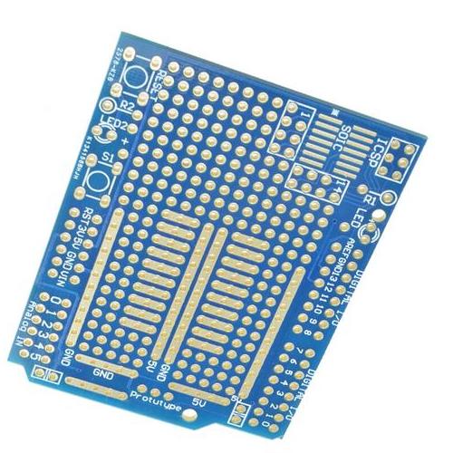
What is a Module PCB?
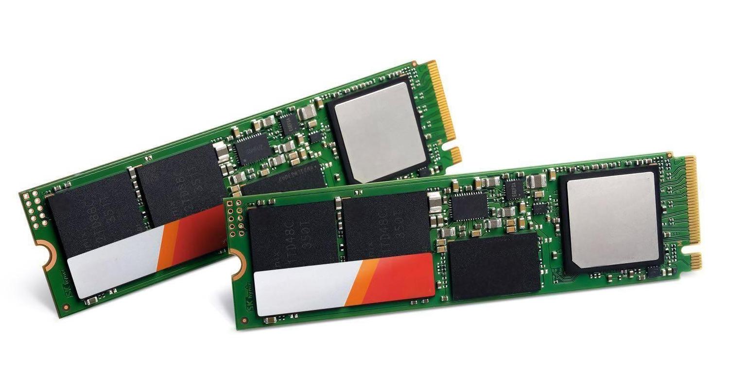
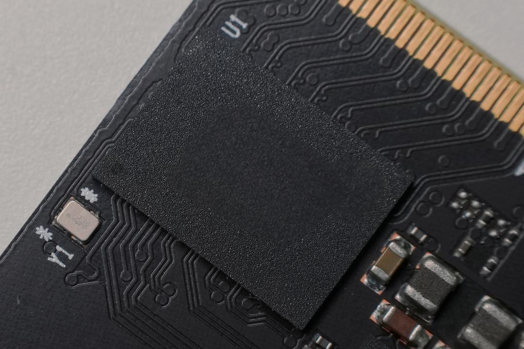
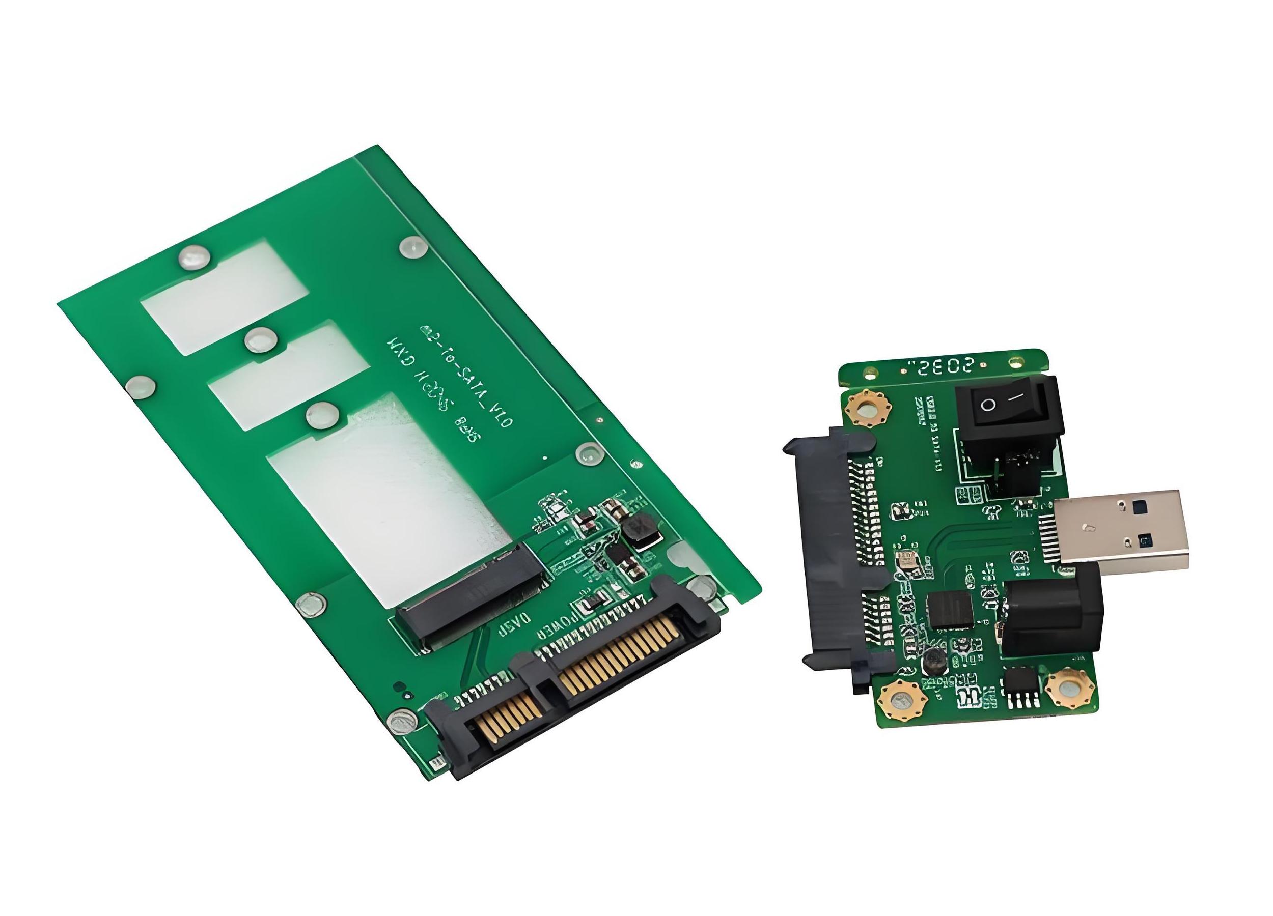
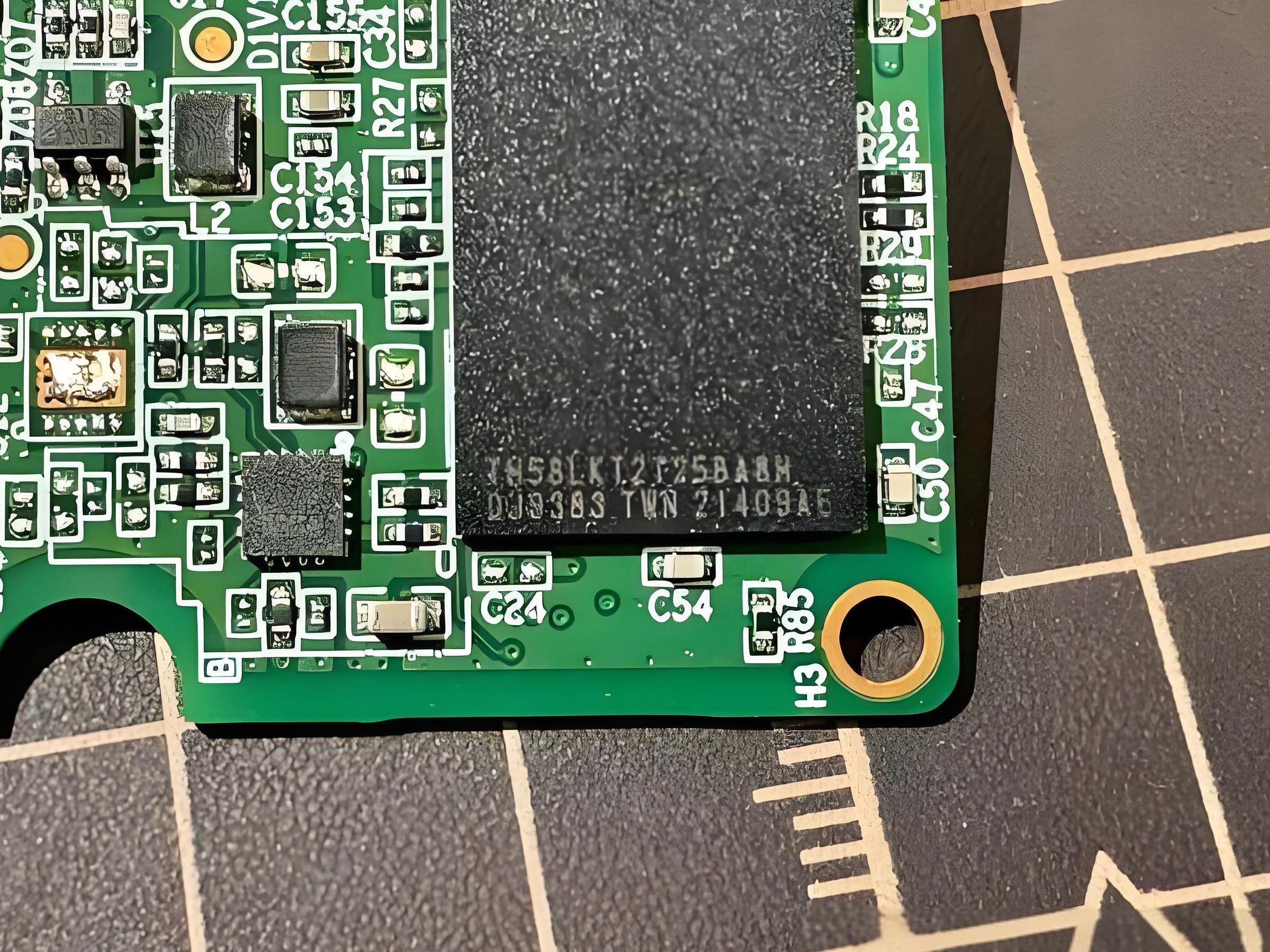
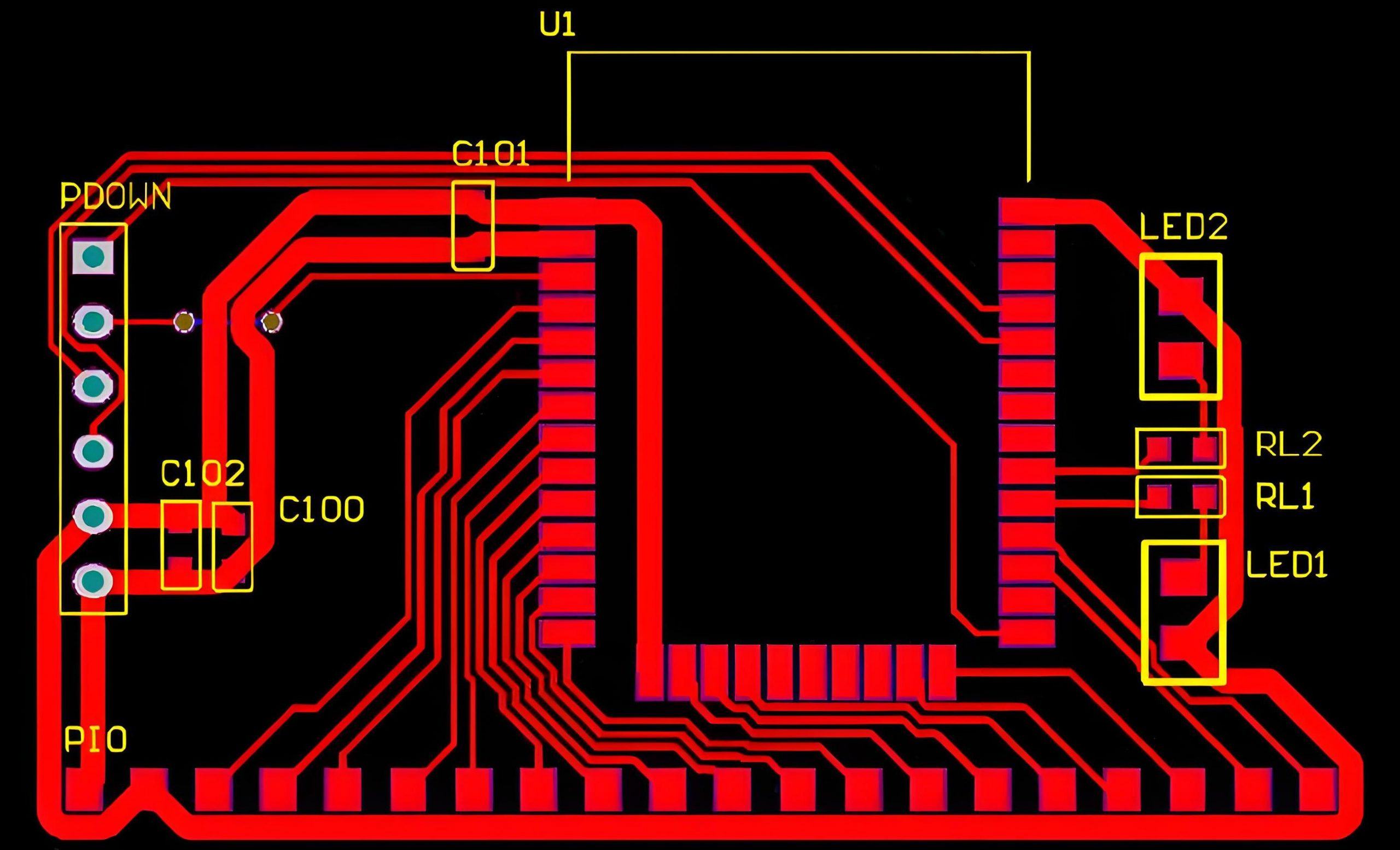
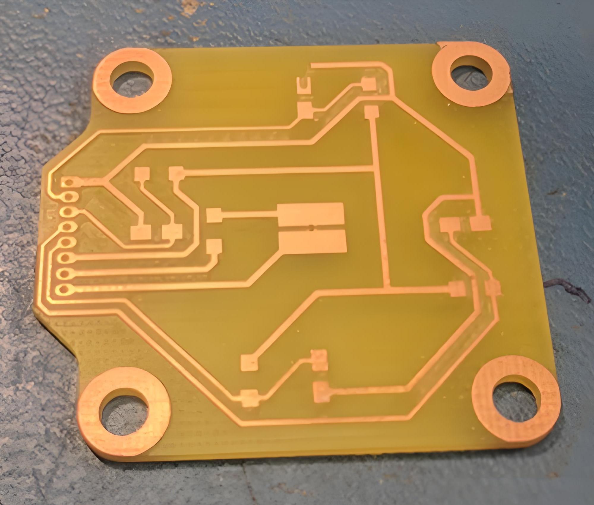
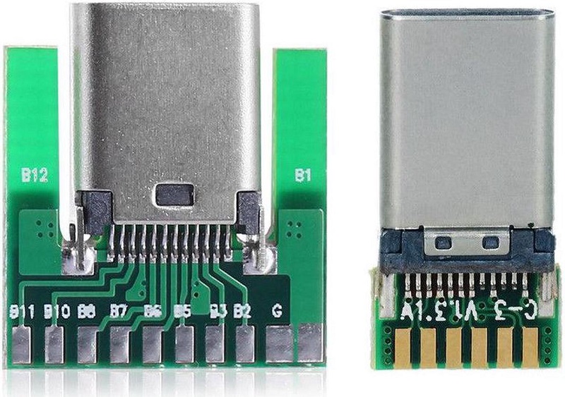
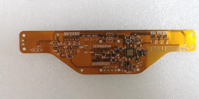
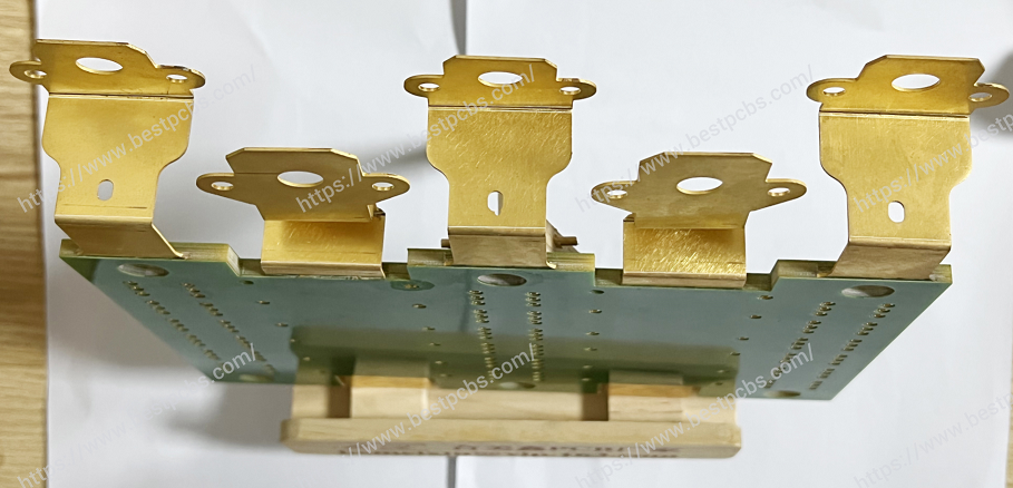
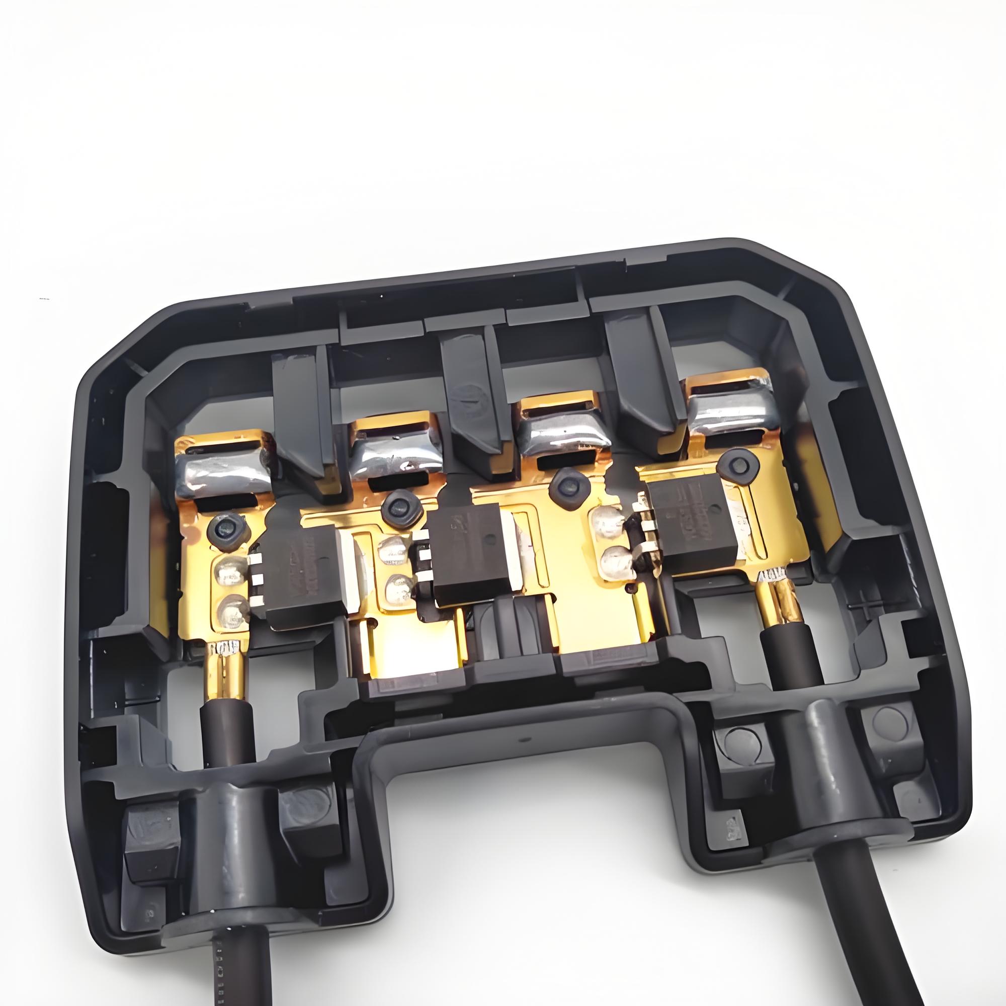
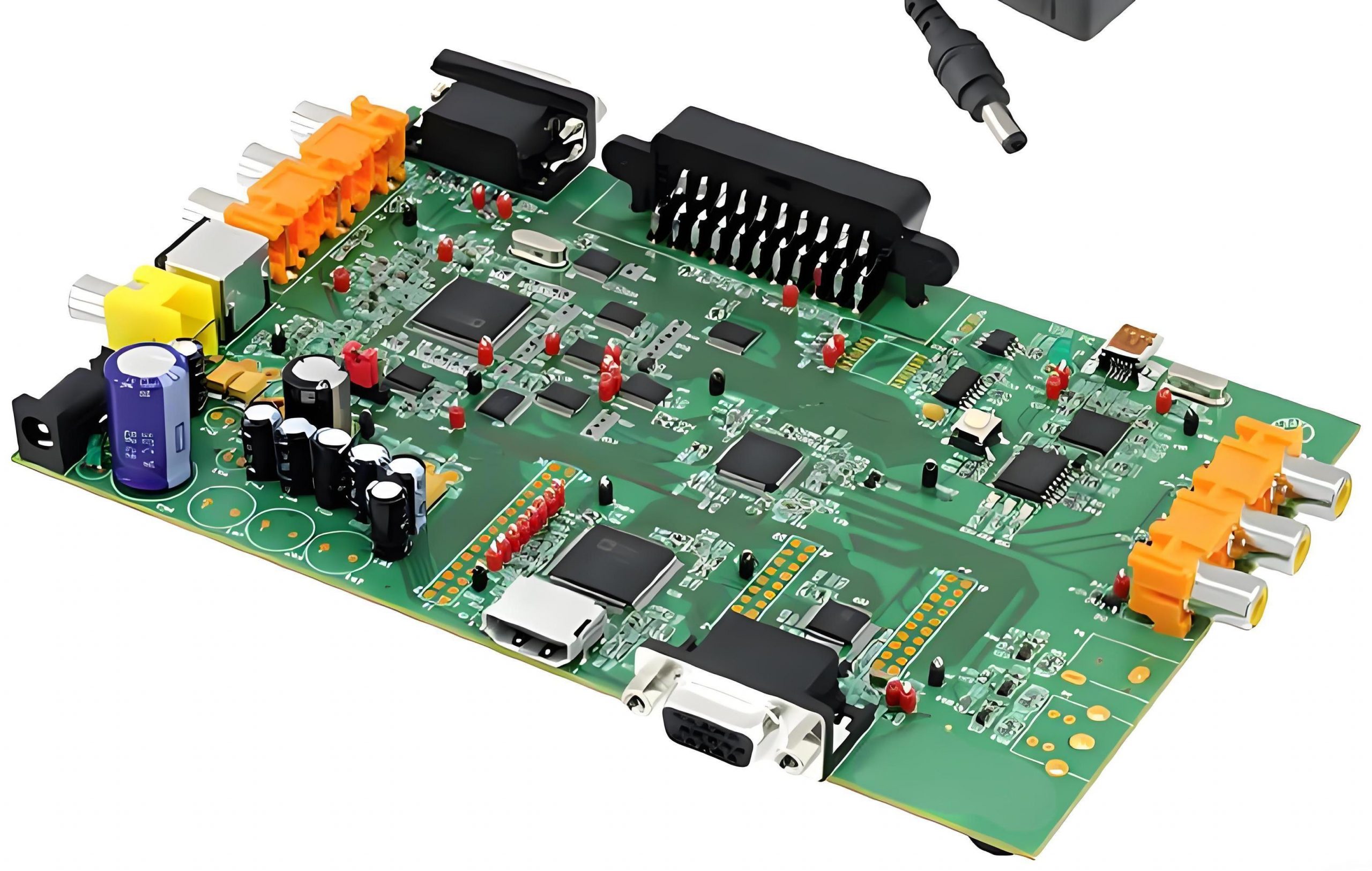
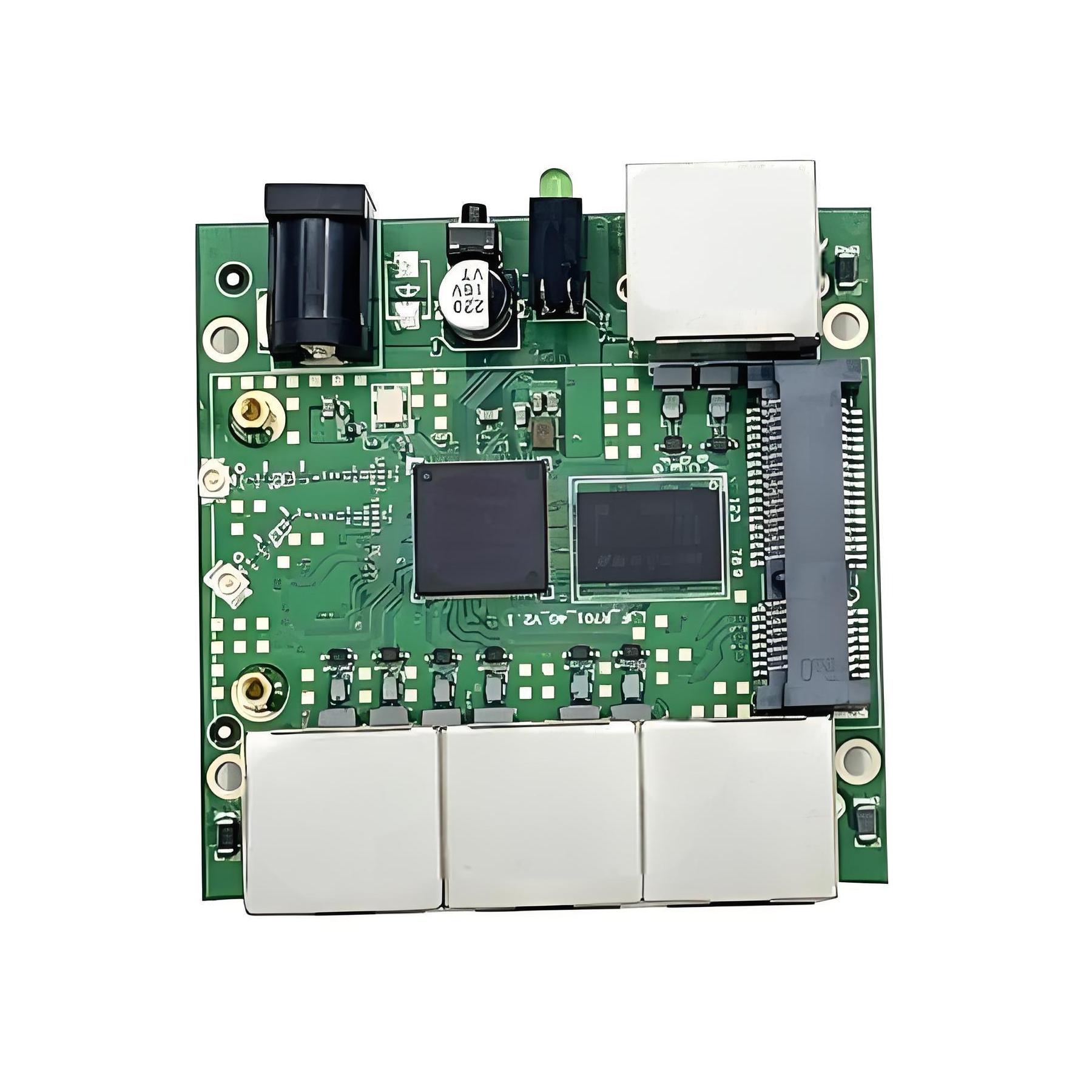
A module PCB (Printed Circuit Board) is the physical platform that houses the components of a wireless module. It is the foundation for the connectivity and functioning of wireless communication systems. Without PCBs, wireless modules would not be able to connect all the essential components, such as microcontrollers, antennas, and sensors, needed for operation.
In simple terms, a module PCB is where the magic happens. It holds the circuit together, providing both mechanical support and electrical pathways for signals to flow. In wireless modules, this PCB ensures that the components are properly connected and function as a single unit. High-quality PCBs are crucial for ensuring that the wireless module performs optimally, with minimal interference or signal loss.
How to Make a PCB Module?
Creating a PCB module involves several steps, each requiring careful attention to detail. Here’s a simplified breakdown:
Design: First, the circuit diagram is designed using specialized software. This diagram maps out how the components will connect, ensuring the module functions as expected.
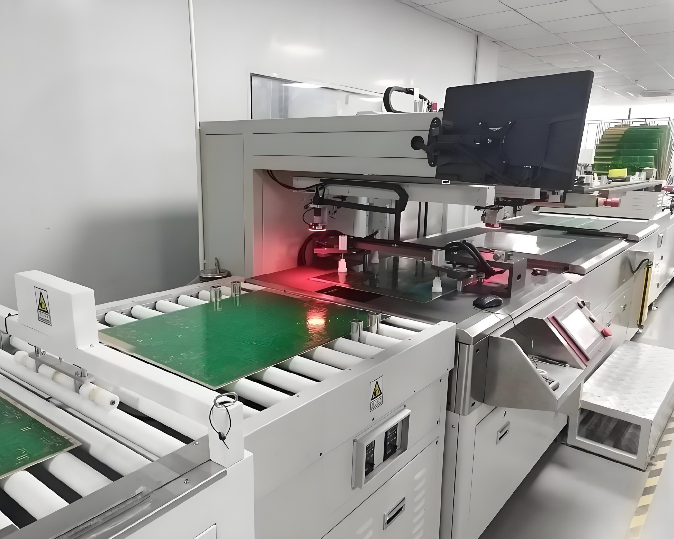
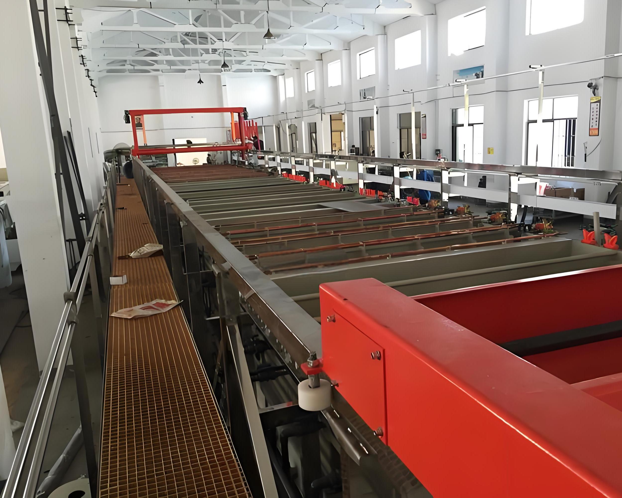
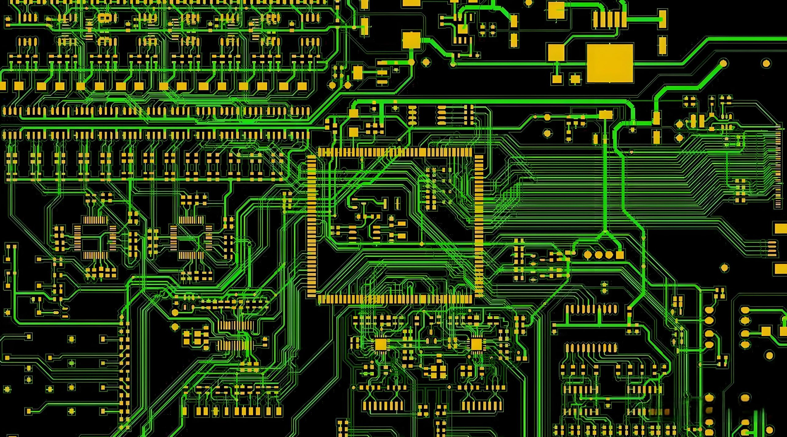
Fabrication: After the design is complete, the PCB is fabricated. This process includes etching copper onto the board, creating the electrical pathways.
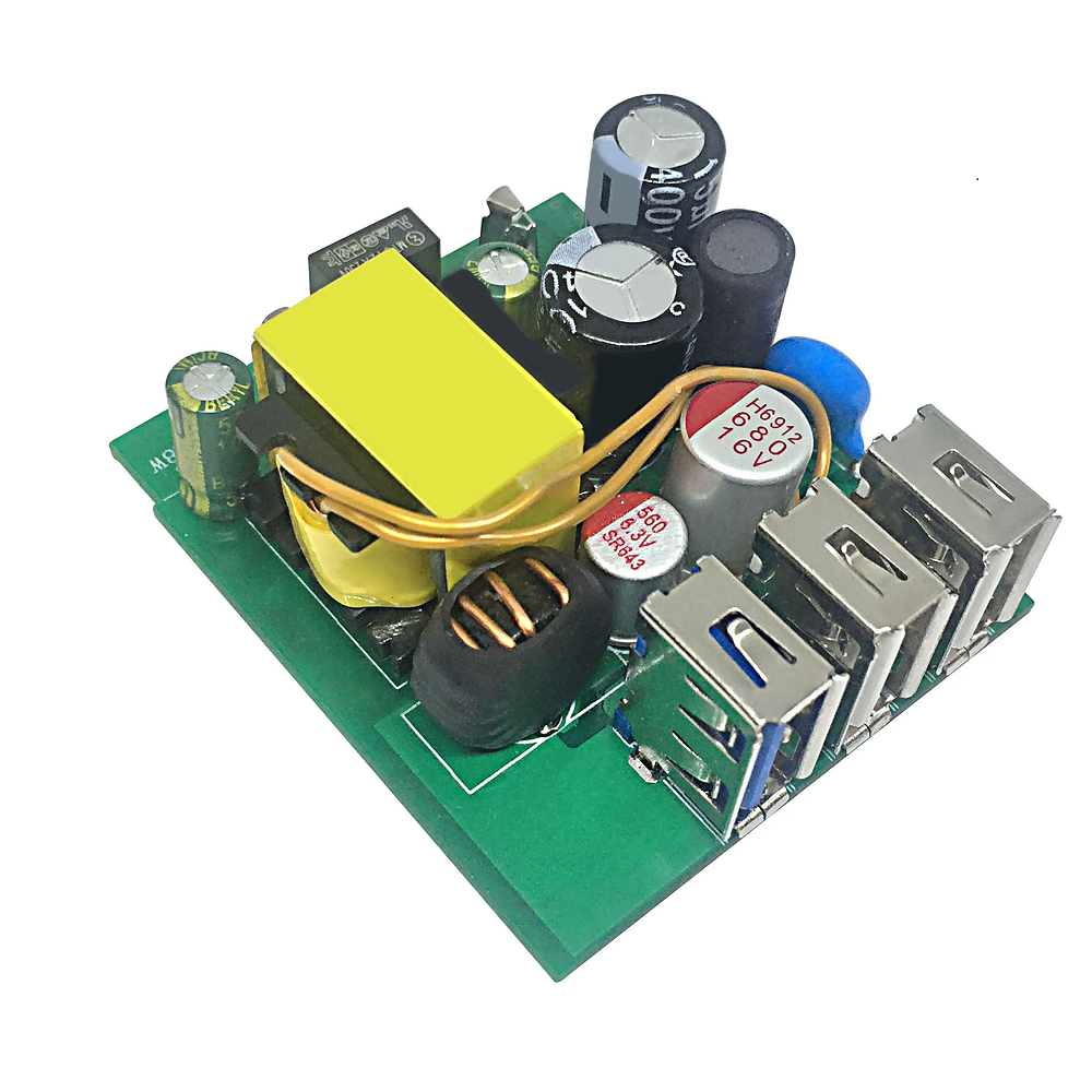
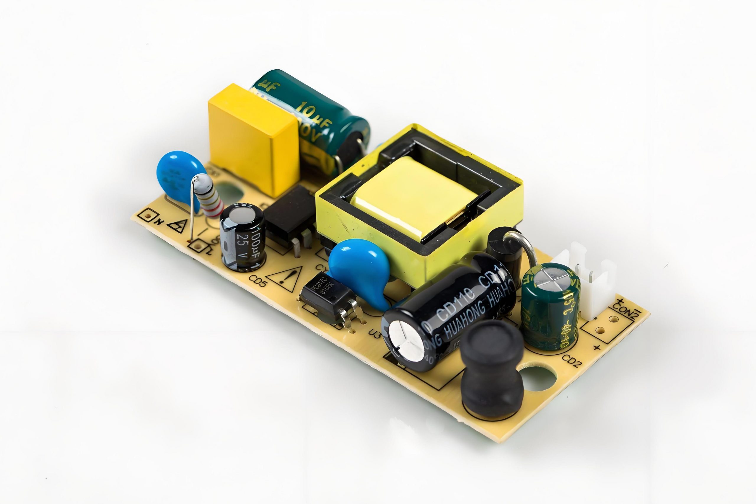
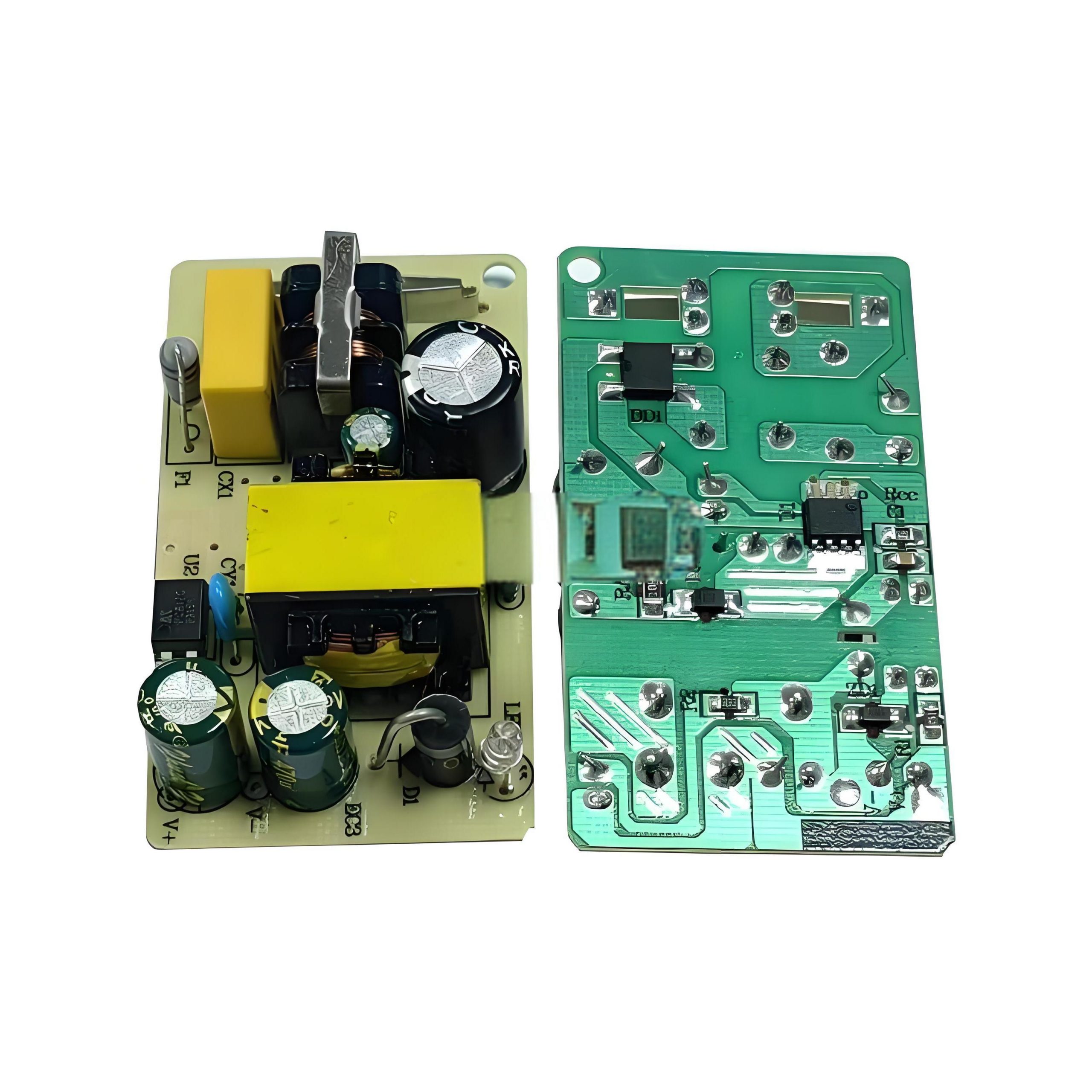
Component Placement: Once the PCB is ready, various components like resistors, capacitors, and microcontrollers are placed onto the board. This is a critical step, as improper placement can lead to performance issues.
Soldering: The components are soldered onto the board to establish permanent connections. Soldering must be precise to ensure strong electrical connections without any shorts or defects.
Testing: Finally, the module is tested to ensure it works as intended. This includes checking signal strength, functionality, and any interference.
How Do Wireless Module PCBs Work in IoT Devices?
Wireless module PCBs are essential in IoT devices because they enable communication between the device and the network. These modules typically integrate multiple communication protocols, allowing IoT devices to connect and exchange data with other smart devices. For instance, a wireless module PCB used in smart farming devices can transmit environmental data, such as temperature and humidity, to a central system where it is analyzed for patterns and trends.
These modules are small, compact, and highly efficient, which makes them ideal for IoT applications that require low-power consumption and reliable performance. In the case of poultry monitoring systems, wireless modules in the form of multisensory bands gather data on bird health, temperature, and movement, transmitting it to farm management systems for real-time decision-making.
What Are the Applications of Wireless Module PCBs in Agriculture?
Wireless module PCBs play a crucial role in modernizing agriculture. They provide the infrastructure for various smart farming solutions, allowing farmers to make data-driven decisions that improve productivity and animal welfare. Here are some key applications:
Smart Irrigation Systems: Wireless modules are used to monitor soil moisture levels and weather conditions, ensuring that crops receive the right amount of water. This reduces waste and increases efficiency.
Livestock Monitoring: Wireless modules integrated into wearable devices like multisensory bands for poultry allow farmers to track the health and activity of their livestock. This data helps in early disease detection, better nutrition, and more efficient herd management.
Precision Farming: By using wireless modules to gather and transmit data, farmers can optimize the use of fertilizers, pesticides, and other inputs, ensuring maximum crop yields with minimal environmental impact.
Environmental Monitoring: Wireless sensors can monitor temperature, humidity, and other environmental factors critical for both crops and livestock. This data is transmitted via wireless module PCBs to central control systems for analysis.
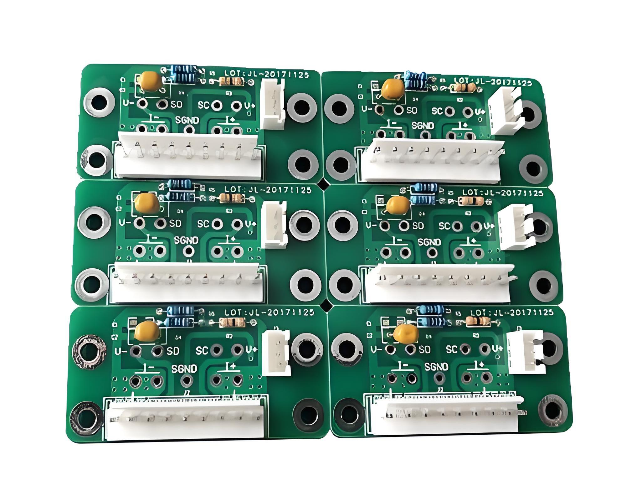
How to Integrate a Multisensory Band into a Wireless Module PCB for Poultry?
Integrating a multisensory band into a wireless module PCB for poultry requires careful design and consideration of several factors. The multisensory band is a wearable device equipped with sensors that monitor various physiological parameters of poultry, such as body temperature, movement, and health status.
To integrate this into the wireless module PCB, the following steps are necessary:
Sensor Selection: Choose the appropriate sensors for monitoring poultry health, such as temperature sensors, motion detectors, and accelerometers. These sensors will provide the data needed for analysis.
PCB Design: Design the PCB to accommodate the sensors, ensuring that the connections are stable and reliable. The board must also support wireless communication protocols like Bluetooth or Zigbee to transmit the data to a central system.
Power Management: Since the multisensory band will likely be worn by poultry, power efficiency is crucial. The PCB must be designed to minimize energy consumption while ensuring the module works for extended periods.
Testing and Calibration: Once integrated, the system must be thoroughly tested to ensure accurate data collection. Calibration of the sensors ensures that the data is precise and reliable.
How Does a Wireless Module PCB Contribute to Smart Poultry Farming?
Smart poultry farming relies heavily on wireless module PCBs to enable real-time monitoring and management of poultry health and behavior. These modules allow for the collection of data from multisensory bands worn by poultry, providing farmers with insights into factors such as temperature, activity levels, and potential health issues.
Wireless modules transmit this data wirelessly to centralized systems, where it can be analyzed and used to make informed decisions. This leads to improved animal welfare, more efficient farm operations, and ultimately, higher productivity. By integrating wireless technology, farmers can reduce labor costs and improve the quality of their products.
What Are the Design Challenges for Wireless Module PCBs?
While designing a wireless module PCB, several challenges must be addressed to ensure its functionality and performance:
Signal Integrity: Wireless communication relies on clean signals, so designers must ensure minimal interference and signal loss.
Size Constraints: For IoT devices and wearable solutions like multisensory bands for poultry, the PCB must be compact while still housing all necessary components.
Power Efficiency: Since many wireless modules are battery-powered, reducing energy consumption is crucial to extend the life of the devices.
Environmental Factors: Wireless modules used in agriculture and poultry farming must be able to withstand harsh environments, including temperature fluctuations, moisture, and dust.
Despite these challenges, the benefits of wireless module PCBs far outweigh the difficulties. With careful planning and innovative design, these modules can power the next generation of smart farming technologies.
In conclusion, wireless module PCBs are revolutionizing agriculture by enabling smart farming solutions that enhance productivity, sustainability, and animal welfare. Through the integration of multisensory bands for poultry, these modules provide farmers with real-time data that improves decision-making and operational efficiency.
As technology continues to evolve, the role of wireless module PCBs in agriculture will only grow, contributing to more sustainable farming practices and smarter, more connected agricultural systems.
At EBest Circuit (Best Technology), we specialize in creating high-performance wireless module PCBs that support the development of innovative solutions like multisensory bands for poultry. Our advanced PCB manufacturing processes ensure that your devices are built to last and operate with optimal efficiency.