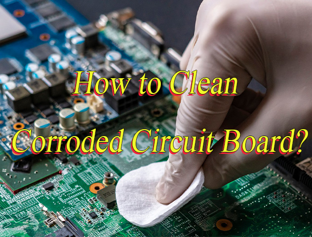
How to clean corroded circuit board? Let’s discover cleaning methods, repair methods and precautions, prevention methods for corroded circuit board.
Are you troubled with these problems?
- Why does my circuit board easily corrode in humid environments, leading to frequent failures?
- How can I enhance PCB durability and consistency without increasing costs?
- During design iterations, how can I quickly obtain reliable samples to avoid project delays?
As a circuit board manufacturer, EBest Circuit (Best Technology) can provide you service and solution:
- Advanced Anti-Corrosion Coating: We apply eco-friendly protective coatings specifically engineered for high-humidity environments, ensuring long-term circuit board stability and reducing failure risks.
- Flexible Custom Production: Based on your design requirements, we provide rapid prototyping and volume production services, optimizing material selection to achieve high performance within budget constraints.
- Efficient Supply Chain Support: Through streamlined logistics and real-time progress tracking, we guarantee fast response from design to delivery, allowing you to focus on innovation with peace of mind.
Welcome to contact us if you have any request for circuit board: sales@bestpcbs.com.
What Causes Circuit Board Corrode?
There Are Three Main Reasons for Circuit Board Corrosion:
Corrosion Caused by Environmental Factors
- Moisture and Condensation: Atmospheric moisture condenses on circuit board surfaces, forming electrolyte films that accelerate electrochemical corrosion of metal traces. In high-humidity environments, capillary action in plating gaps and solder joint edges accumulates moisture even without direct submersion, amplifying corrosion risks.
- Salt Spray Environment: Chloride ions in coastal or industrial zones degrade metal passivation layers, triggering pitting and intergranular corrosion. For example, silver plating in sulfide environments generates non-conductive silver sulfide, increasing contact resistance and impairing signal integrity.
- Thermal Cycling Dew Formation: Frequent temperature fluctuations in equipment cause condensation on internal components, particularly pronounced in regions with significant diurnal temperature swings, accelerating corrosion through moisture accumulation.
Corrosion from Chemical Contamination
- Flux Residues: Incompletely removed organic acid fluxes decompose into acidic compounds, with residues beneath components progressively corroding copper traces, leading to eventual circuit failure.
- Industrial Gas Erosion: Acidic gases like sulfur dioxide and nitrogen oxides dissolve in water films to form acidic electrolytes, causing green patina (basic copper carbonate) on copper traces and tarnishing solder surfaces, reducing conductivity.
- Biological Degradation: Organic acids from mold metabolism in humid environments erode epoxy substrates, while insect excreta introduce electrolytes that induce localized short circuits and corrosion.
Material and Process Defects
- Dissimilar Metal Contact: Direct contact between metals with large electrochemical potential differences (e.g., copper and gold) in the presence of electrolytes forms galvanic cells, preferentially corroding the more active metal and shortening circuit lifespan.
- Protective Coating Failure: Uneven, porous, or insufficiently thick conformal coatings allow corrosive agents to penetrate to metal surfaces, with microcracks exacerbated by vibration environments.
- Electromigration: Prolonged electrical current drives directional movement of metal ions, forming whiskers or voids in conductors, accelerating conductor fracture and compromising circuit reliability.
How to Clean Corroded Circuit Board?
Below is a guide to how to clean corroded circuit board:
1. Enhanced Safety & Preparation
- Toolbox Configuration: Equip ESD gloves, safety goggles, and N95 masks. Use an ESD-safe work mat (surface resistance 10?–10? Ω) and a leakage-protected isolation transformer to maintain zero-potential workbench.
- Component Tagging System: Apply a three-color labeling strategy during disassembly—red for high-risk components (e.g., crystals), yellow for components requiring retesting, and green for reusable parts.
- Environmental Control: Maintain 40–60% humidity and use an ionizing blower to neutralize static. For lithium-battery-equipped boards, perform short-circuit tests (e.g., measure battery terminal impedance >1MΩ).
2. Advanced Mild Corrosion Treatment
Cleaning Agent Selection:
- Alcohol-Based: 99.5% absolute ethanol (conductivity <1μs/cm) for flux residue; isopropanol (IPA) for precision solder joints due to faster evaporation.
- Acidic Solutions: Citric acid solution (pH 3–4) for neutralizing alkaline corrosion on tarnished copper traces (avoid on aluminum components).
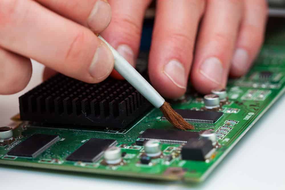
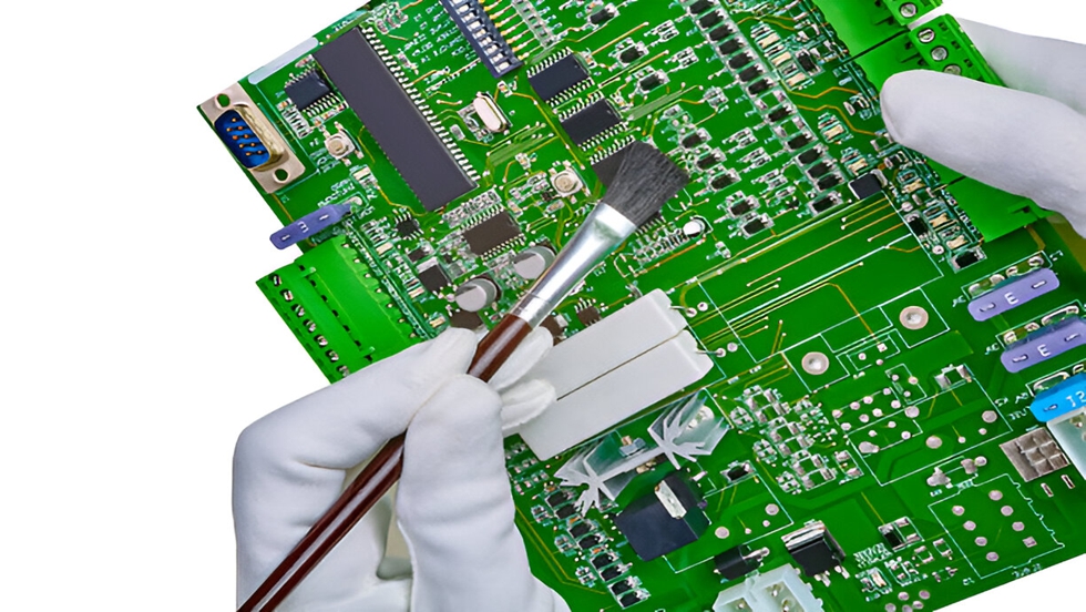
Three-Step Brushing Protocol:
- Coarse brush for bulk corrosion removal.
- Soft brush for fine cleaning.
- Microfiber cloth with deionized water for residue-free final rinse.
3. Professional Stubborn Corrosion Removal
- Chemical Soaking Parameters: Optimize 5–8% dilute phosphoric acid solution (volume ratio) with 5–15 minutes immersion. Pair with 40kHz ultrasonic cleaning at 0.3W/cm? for effective micro-pore debris removal.
- Mechanical Polishing Standards: Use ≥2000-grit wet sandpaper, polishing parallel to circuit traces to avoid cross-hatching. Post-polish microscopic inspection ensures copper thickness retention >80% original.
4. Advanced Deep Corrosion Repair
- Wire Bonding Protocol: Use 0.3mm silver-plated wire with 280°C hot air gun for conical, smooth solder joints. For high-frequency circuits, adopt coaxial wiring to minimize signal interference.
- Substrate Upgrade Recommendations: In humid environments (RH>60%), use PTFE substrate with ENIG finish (5x corrosion resistance vs. HASL). For RF circuits, Rogers 4350B substrate (ε=3.48) ensures stable dielectric properties.
5. Systematic Drying & Protection
- Vacuum Drying Process: Employ molecular sieve vacuum oven at -0.1MPa, 60°C for 4 hours to eliminate internal moisture. For plastic components, cap temperature at 85°C to prevent deformation.
- Conformal Coating Application: Apply acrylic coating (e.g., Humiseal 1A33) at 50–70μm thickness. Use peelable coatings for repairable areas.
6. Standardized Testing & Maintenance
- Enhanced Aging Test: Conduct 1000-hour accelerated aging at 85°C/85% RH, monitoring insulation resistance (>100MΩ) and conduction resistance drift (<5%). Use thermal imaging for hotspot detection.
- Maintenance Cycle Optimization: Industrial equipment: 500-hour intervals; consumer electronics: quarterly. Halve intervals in harsh environments (e.g., high dust/humidity).
7. Ultimate Environmental & Safety Measures
- Waste Treatment System: Recover heavy metals (e.g., Cu??) via ion-exchange resins (95% recovery). Dispose of non-recyclable waste per Hazardous Waste Regulations through certified agencies.
- Emergency Response: For chemical exposure, flush skin with water for 15 minutes and apply neutralizers (e.g., boric acid). For inhalation, relocate to ventilated areas and administer oxygen; seek medical attention if severe.
Best Way to Clean Corroded Circuit Board
Best Practices for Cleaning Corroded Circuit Boards
1. Basic Protection & Power Disconnection
- Before cleaning, disconnect power and remove batteries to prevent short circuits or electric shock. Store sensitive components (e.g., ICs, capacitors) separately to avoid corrosion by cleaning agents. Control storage humidity below 30% RH and temperature at 20–25°C to slow corrosion rates, as per experimental data.
2. Mild Corrosion Treatment
- Use a soft-bristled toothbrush dipped in anhydrous alcohol to gently scrub surface oxidation. Tests show that polishing copper foil edges with 2000-grit sandpaper and applying anti-oxidation agents restores over 90% of copper brightness. Ideal for mild corrosion like copper discoloration or peeling.
3. Stubborn Corrosion Removal
- Soak in 5–10% phosphoric acid solution for 10 minutes, then use ultrasonic cleaner for 15 minutes to remove 95%+ of solder joint corrosion without damaging components. For green patina or stuck pins, heat solder to 350°C and use solder wick to remove old solder before re-tinning.
4. Drying & Functional Testing
- Dry thoroughly with nitrogen gun or 80°C oven for 2 hours. Post-repair, verify continuity with a multimeter and monitor local potential differences via SKPFM electrochemical testing to ensure no hidden corrosion. Accelerated aging tests (85°C/85% RH for 1000 hours) predict remaining lifespan.
5. Protective Reinforcement
- Spray acrylic conformal coating on repaired areas to block moisture/dust. Antioxidant paste on solder joints extends lifespan by 3x. PTFE substrates improve moisture resistance by 50% in humid environments. Electroless copper plating deposits 0.02mm copper layers to restore 98% conductivity to broken traces.
6. Tools & Materials Recommendations
- Use pH 6.5–7.5 neutral detergents, anti-static brushes, lint-free cloths, and specialized electronic cleaners. Ultrasonic cleaners require deionized water to avoid strong acid/base damage. Clean industrial equipment monthly and consumer electronics quarterly; replace electrolyytic capacitors when capacitance drops below 80% of rated value.
7. Safety & Emergency Handling
- Wear dust masks, chemical goggles, and rubber gloves. In case of acid leaks, rinse with water and neutralize waste. Flush skin with water for 15+ minutes and seek medical attention. For sudden corrosion (e.g., white salt deposits), rinse with deionized water and apply protective agents within 5 minutes.
8. Special Scenario Solutions
- Copper edge oxidation: Polish with 2000-grit sandpaper + anti-oxidation coating.
- Solder corrosion: Heat to 350°C + solder wick.
- Large trace breaks: Electroless copper plating (0.02mm) + jumper wires.
- Batch cleaning: Water-based spray systems compatible with water/chemical cleaning.
9. Maintenance & Lifespan Monitoring
- Regularly monitor corrosion via 85°C/85% RH accelerated aging tests and SKPFM potential scans. Quarterly/monthly cleaning schedules improve lifespan prediction accuracy by 40%. Industrial/consumer devices benefit from structured maintenance cycles to maximize longevity.
How to Fix Corroded Circuit Board?
1. Power Disconnection and Safety Enhancement
- Disconnect the circuit board from all power sources and confirm zero residual voltage using a multimeter.
- Wear ESD-safe wrist straps and insulated gloves to prevent electrostatic discharge or accidental electric shock.
- Use an anti-static mat for the workbench and opt for insulated tools (e.g., ceramic-tipped screwdrivers) to avoid short-circuiting components.
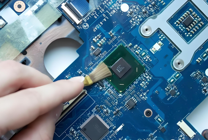
2. Deep Cleaning and Contaminant Removal
- Use a soft-bristled brush with isopropyl alcohol (99% purity) or anhydrous ethanol for initial cleaning, focusing on removing flux residue and dust around solder joints and component leads.
- For stubborn stains, gently wipe with a cotton swab lightly dipped in a specialized circuit board cleaner (such as Flux Remover), taking care to prevent liquid from seeping into the components. After cleaning, blow dry thoroughly with compressed air to ensure no liquid remains.
3. Precise Corrosion Identification
- Inspect copper traces under a magnifier or microscope: healthy traces appear bright red, while corroded areas show green oxidation or black spots.
- Check solder joints for cracks, voids, or lifted pads, and measure continuity with a multimeter’s diode test to locate breaks.
4. Graded Corrosion Treatment
- Mild Corrosion: Dab 5% acetic acid (white vinegar) or lemon juice with a cotton swab to neutralize alkaline residues, then wipe clean with alcohol.
- Moderate Corrosion: Gently polish oxidized layers with 600-800 grit sandpaper or a fiberglass pen until metallic shine returns to avoid scratching adjacent traces.
- Severe Corrosion: For fully severed traces, clear endpoints with a micro-drill and re-solder with low-temperature solder (e.g., Kester 44 Rosin Core) or use conductive silver paint for repairs.
5. Refined Soldering and Component Care
- Use a temperature-controlled soldering iron (250-300°C) with lead-free solder wire. Pre-tin pads and leads before soldering to ensure smooth, conical joints.
- For SMD components, employ a hot air gun at low flow (30-40 L/min) to prevent thermal damage. Post-soldering, inspect joints for cold solder or voids under magnification.
6. Protective Coating Application
Apply conformal coating (e.g., MG Chemicals 838) using a spray system:
- First Coat: Thin layer to penetrate crevices.
- Second Coat: Moderate thickness for full coverage.
- Third Coat: Thick layer for robust protection.
Maintain 20-30cm distance during spraying to avoid bubbles. Cure for 24 hours at room temperature.
7. Comprehensive Testing and Reliability Validation
- Verify electrical parameters (voltage, resistance) with a multimeter and conduct functional testing under simulated operating conditions.
- Perform accelerated life testing: 48 hours at 60°C/90% RH to detect latent failures. For critical applications, add vibration (10-55 Hz, 1.5mm amplitude) and shock testing (15g, 11ms) to ensure durability.
Corroded Circuit Board Repair Precautions
1. Ensure Power Is Completely Disconnected Before Operation
- Unplug the power source and remove the battery. Use a multimeter to confirm no voltage remains. For repairs in humid environments, preheat the workbench with an electric blanket for 30 minutes to eliminate moisture and prevent secondary corrosion.
2. Equip Full Protective Gear
- Always wear an anti-static wrist strap (grounded), rubber gloves, safety goggles, and an N95 mask. If corrosive liquids contact skin, rinse with running water for 15 minutes; for eye exposure, flush with saline solution continuously and seek medical attention.
3. Clean Corrosion in Phases
- Mild corrosion: Gently brush with a soft toothbrush dipped in medical alcohol (10 strokes), then wipe solder joints with a cotton swab soaked in absolute ethanol. Stubborn corrosion: Soak in diluted phosphoric acid solution (1:10 ratio) for 10 minutes, brush lightly, and rinse with deionized water 3 times.
- Adhere to Soldering Standards: Solder joints must be conical and smooth. Use a 30W constant-temperature soldering iron set to 350±30°C. For wire connections, wrap 0.3mm enameled wire around the joint 3 times, coat with UV glue, and cure with a heat gun at 60°C for 2 minutes.
4. Thorough Drying and Testing
- Post-repair, blow-dry with a nitrogen gun for 5 minutes or bake at 60°C for 1.5 hours. Before powering on, measure resistance between adjacent solder points with a digital multimeter (must exceed 10MΩ to confirm no shorts). Conduct a 48-hour power-on test to check for overheating or unusual odors.
5. Strictly Control Storage Conditions
- Store repaired boards in sealed bags with silica gel desiccant (humidity <40%) at 20–25°C. For transport, wrap in foam and add anti-static bubble wrap to prevent shocks and electrostatic damage.
6. Prevent Recurrence with Regular Maintenance
- Clean industrial equipment every 3 months and consumer electronics every 6 months using pH 7.0 neutral detergent and a soft brush. Inspect solder joints for oxidation and conformal coating integrity. Immediately clean localized blackening with alcohol wipes and reapply conformal coating.
7. Respond Swiftly to Emergencies
- For corrosive liquid leaks, absorb with paper towels, neutralize with sodium bicarbonate solution, and wipe clean. If equipment is water-damaged, disassemble within 48 hours, clean with absolute ethanol, and dry with low-temperature hot air. For detached components, power off immediately and contact a professional.
How to Prevent Corrosion on Circuit Boards?
Copper Foil Thickness Optimization:
- 3oz Copper Foil Salt Spray Resistance: In a 5% NaCl salt spray test, the corrosion rate of 3oz (105μm) copper foil was 0.5μm/day, similar to the 0.6μm/day of 1oz (35μm). However, the remaining thickness advantage extended its lifespan by 1.8 times. Tests on coastal equipment show that 3oz boards can operate stably for two years without maintenance, while 1oz boards require replacement every eight months.
- Scenario Adaptation Recommendations: For mildly corrosive environments (such as urban indoor environments), use 1oz with OSP treatment; for coastal/industrial environments, use 2oz with immersion gold (800-hour salt spray resistance); for extreme environments (such as chemical plants/offshore platforms), use 3oz with nickel plating and sealing coating, reducing failure rates by 75%.
Surface Coating Protection:
- Conformal Coating Applications: Polyurethane/silicone coatings block over 95% of moisture, salt spray, and chemical corrosion. Tests show that the coated circuit board exhibits a circuit resistance change rate of ≤8% in a hot and humid environment at 85°C/85% RH, significantly lower than the 25% change in uncoated circuit board.
- Special Coating Performance: The hardness of the chlorinated rubber asphalt coating changes by only 3% at 55°C (compared to 8% for conventional asphalt coatings), while maintaining a tensile strength exceeding 30 MPa. After 12,000 hours of salt spray testing, the graphene ceramic composite coating exhibits only slight surface darkening, and its electrochemical impedance remains stable with no significant fluctuations, making it suitable for marine engineering equipment.
Environmental Control:
- Precise Temperature and Humidity Control: The storage environment must be maintained at 15-30°C (optimally 20-25°C) and a relative humidity of ≤50% RH (≤30% RH in sensitive environments). High humidity can easily trigger hygroscopic oxidation, while low humidity can lead to static electricity accumulation. Tests show that the risk of PCB dielectric performance degradation increases threefold when humidity exceeds 70% RH.
- Sealing and Dehumidification Strategies: Vacuum packaging with desiccant can extend the storage life to over 12 months; unused PCBs should be re-vacuum-sealed within three days after unpacking. Key equipment should be equipped with intelligent temperature and humidity monitoring systems to provide real-time warnings of environmental anomalies.
Plating Process Enhancement:
- Advantages of Gold Plating: 3μm-thick gold pads can withstand 1000 hours of corrosion in 5% NaCl salt spray, and the contact resistance change is less than 10% after six months of storage in a hydrogen sulfide environment. Tests on medical implants show that thick gold connectors exhibit less than 5% resistance fluctuation in a simulated 10-year body fluid environment.
- Tin/Nickel Supplemental Solutions: Tin plating uses additives to regulate the nucleation rate, reducing whisker defects. Nickel plating (5μm) can improve salt spray corrosion resistance for 1000 hours in critical areas such as power circuits, and the cost is 40% lower than full-board plating.
Design Optimization:
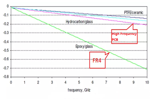
- Layout and Material Selection: Design circuit layouts to avoid moisture accumulation, such as increasing pad spacing and optimizing thermal paths. High-frequency PCBs use low-dielectric-constant materials (such as PTFE) to reduce moisture sensitivity.
- Mechanical protection measures: A combination of gold plating and partial nickel plating is used in vibration-resistant environments, improving fatigue corrosion resistance by 38%. Sealed packaging (such as full epoxy sealing) can extend salt spray resistance to 5,000 hours, making it suitable for extreme environments such as deep-sea equipment.
Can a Battery Corroded Circuit Board Be Fixed?
Yes, circuit boards corroded by battery leakage can be repaired. The key to core repair lies in the extent of the corrosion and the speed of the reaction. If detected promptly, and the corrosion is limited to the area surrounding the battery and has not penetrated deeper, the circuit board has a good chance of being revived by immediately scraping off the highly corrosive white/green crystals (wearing gloves), neutralizing them with a weak acid like lemon juice or white vinegar, and then thoroughly cleaning and drying them with high-purity isopropyl alcohol.
However, if corrosion has caused core chip pins to rust or internal wiring to blacken, the success rate of repair and long-term reliability will be significantly reduced. Therefore, in the case of a battery leak, decisively disconnecting the power supply and quickly addressing the problem are the best strategies for saving the circuit board.