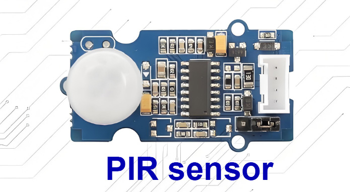
If you’ve ever walked into a room and had the lights turn on automatically, or relied on a home security system to detect intruders, you’ve experienced the work of PIR (Passive Infrared) sensors. These small but powerful devices are everywhere—from smart homes to industrial settings—thanks to their low power consumption, affordability, and reliable motion detection. But for many people, understanding how PIR sensors work, choosing the right one, and troubleshooting common issues can be a challenge. In this guide, we’ll break down everything you need to know about PIR sensors, from their basic mechanics to advanced applications, so you can use them effectively in your next project or system.
What Is a PIR Sensor? Understanding the Basics
First, let’s clarify what PIR sensors are and why they’re so widely used. PIR stands for Passive Infrared, which means these sensors don’t emit any energy themselves (unlike active sensors like microwave detectors). Instead, they passively detect changes in infrared radiation (heat) in their surrounding environment. All warm-blooded creatures, including humans, emit infrared radiation in the 8-14 µm wavelength range—and PIR sensors are specifically designed to detect this range.
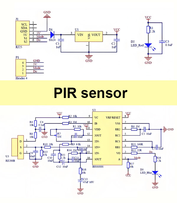
The core component of a PIR sensor is a pyroelectric element, a material that generates an electrical charge when exposed to changes in temperature. Most PIR sensors use a dual-element design, which helps reduce false triggers by comparing radiation levels between two adjacent areas. When a moving heat source (like a person) passes through the sensor’s field of view, it causes a temperature change in one element before the other, generating a signal that the sensor interprets as motion.
How Do PIR Sensors Work? A Step-by-Step Explanation
To fully leverage PIR sensors, it’s important to understand their operating mechanism. Here’s a simplified breakdown of how they detect motion:
The Role of Fresnel Lenses
Nearly all PIR sensors come with a Fresnel lens—a thin, grooved plastic lens that serves two key purposes. First, it focuses infrared radiation onto the pyroelectric element, boosting the sensor’s sensitivity. Second, it divides the sensor’s detection area into multiple “zones” (or fields of view). When a heat source moves from one zone to the next, it creates a pattern of changing temperatures that the sensor can recognize as motion.
Signal Processing and Output
Once the pyroelectric element detects a temperature change, it produces a tiny electrical signal. This signal is sent to an integrated circuit (ASIC) within the sensor module, which amplifies the signal and filters out noise (like small temperature fluctuations from sunlight or wind). If the signal meets the sensor’s pre-set criteria (e.g., sufficient amplitude and duration), the sensor outputs a digital signal (high or low voltage) that can trigger an action—such as turning on a light or activating an alarm.
Key Technical Specifications of PIR Sensors to Consider
When choosing a PIR sensor for your project, understanding its technical specifications is critical to ensuring it meets your needs. Here are the most important specs to look for:
Detection Range and Angle
Detection range refers to the maximum distance at which the sensor can detect motion, typically ranging from 3 meters to 17 meters (or more for industrial models). Detection angle (usually 90° to 120°) describes the width of the area the sensor can cover. Lenses play a big role here—long-distance lenses are ideal for outdoor security, while wide-angle lenses work better for indoor spaces like hallways.
Power Consumption and Voltage
One of PIR sensors’ biggest advantages is their low power consumption, making them perfect for battery-powered devices. Standby current can be as low as 1 µA for ultra-low-power models (like Panasonic’s EKMB series), enabling battery life of up to 10 years. Most PIR modules operate on 3.3V to 20V DC, so be sure to match the sensor’s voltage requirements to your power source.
Response Time and Delay
Response time is how quickly the sensor reacts to motion (usually milliseconds to seconds), while the “time delay” (or “hold time”) is how long the sensor’s output remains active after motion stops. Many PIR modules have adjustable delay settings (from a few seconds to several minutes) to fit different applications.
Common Applications of PIR Sensors Across Industries
PIR sensors are incredibly versatile, with uses spanning residential, commercial, and industrial settings. Here are some of the most popular applications:
Home and Commercial Lighting Control
One of the most common uses of PIR sensors is automatic lighting control. They’re used in hallways, bathrooms, garages, and outdoor spaces to turn lights on when someone enters and off when the area is empty—saving energy and improving convenience.
Security Systems and Intrusion Detection
PIR sensors are a staple in home and business security systems, triggering alarms or activating security cameras when unauthorized motion is detected. Wireless PIR sensors are particularly popular for this application, as they’re easy to install without wiring.
Smart Home and IoT Integration
In smart homes, PIR sensors integrate with IoT devices to create automated scenes—such as turning on the air conditioner when someone enters a room or activating a smart display when motion is detected. They’re also used to monitor room occupancy, helping optimize energy use in smart buildings.
Industrial and Specialized Uses
In industrial settings, PIR sensors detect personnel entering dangerous areas (triggering safety alerts) or monitor equipment status. They’re also used in wildlife trail cameras to capture images when animals pass by, and in pandemic-related applications like activating disinfectant displays.
How to Choose the Right PIR Sensor for Your Project
With so many PIR sensor options available, selecting the right one can be overwhelming. Follow these steps to narrow down your choices:
Define Your Application
Start by clarifying your use case. Are you building a battery-powered security device? You’ll need an ultra-low-power sensor. Do you need to detect motion in a large outdoor area? Look for a long-range sensor with a narrow-angle lens.
Consider the Environment
Indoor sensors don’t need to withstand extreme weather, but outdoor sensors should be weather-resistant and able to handle temperature fluctuations (-20°C to +70°C or wider). Avoid sensors with low temperature thresholds (below 2°C) for cold environments, as they may struggle to detect heat sources.
Evaluate Sensor Quality and Brand
Choose sensors from reputable brands like Panasonic (with their PaPIRs series, which has produced over 100 million units) to ensure reliability. High-quality sensors have better noise immunity and fewer false triggers, saving you time on troubleshooting.
Step-by-Step Guide to Installing a PIR Sensor
Proper installation is key to getting the most out of your PIR sensor. Follow these best practices for optimal performance:
Choose the Right Location
Install the sensor in a location with a clear field of view—avoid obstructions like curtains, plants, or furniture. Keep it away from heat sources (heaters, radiators, direct sunlight) and air vents, as these can cause false triggers. For security applications, mount the sensor at a height of 2-2.5 meters to cover a wider area.
Adjust Sensitivity and Delay
Most PIR modules have potentiometers for adjusting sensitivity and delay. Test the sensor after installation: if it’s triggering too often (e.g., from pets or wind), reduce the sensitivity. If it’s not detecting motion consistently, increase the sensitivity or adjust the angle.
Ensure Proper Wiring (for Wired Sensors)
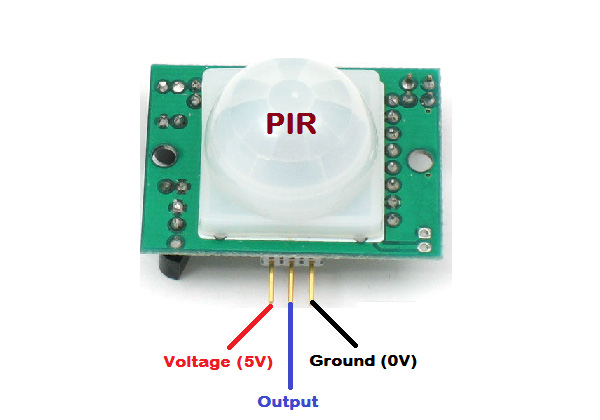
For wired PIR sensors, double-check the wiring: the sensor’s output pin should connect to your microcontroller (e.g., Raspberry Pi) or relay. Use a stable power supply—unstable voltage can cause the sensor to malfunction. If using a battery, choose a high-quality battery to avoid voltage drops.
Top Tips for Optimizing PIR Sensor Performance
Even the best PIR sensor can underperform if not optimized. Here are some expert tips to improve reliability and reduce false triggers:
Clean the lens regularly: Dust and dirt on the Fresnel lens can block infrared radiation, reducing sensitivity.
Use hardware filtering: Add an RC low-pass filter to the sensor’s output to reduce high-frequency noise.
Implement software debouncing: In your microcontroller code, use delay or multiple sampling to confirm motion before triggering an action.
Allow warm-up time: After powering on, PIR sensors need 30 seconds to 1 minute to calibrate to the environment—avoid testing during this period.
Common PIR Sensor Issues and How to Troubleshoot Them
From false alarms to no detection, PIR sensors can experience a range of issues. Here’s how to diagnose and fix the most common problems:
False Triggers
False triggers are the most common issue with PIR sensors. Possible causes include heat sources (sunlight, heaters), air drafts, RF interference (from Wi-Fi routers or microwaves), or moving objects (curtains, plants). To fix this: move the sensor away from these sources, reduce sensitivity, or use a sensor with better noise immunity.
No Motion Detection
If the sensor isn’t detecting motion, check the following: 1) Wiring: Ensure the output pin is connected correctly (common mistake with Raspberry Pi projects). 2) Lens obstruction: Clean the lens and remove any obstacles. 3) Sensitivity: Increase the sensitivity setting. 4) Power supply: Check for voltage drops or dead batteries.
Sensor Won’t Wake Up (Post-Delay)
Some users report that their PIR sensor doesn’t reactivate after the delay period (e.g., a monitor stays off even when motion is detected). This is often a wiring or code issue. Double-check the sensor pin assignment in your code (e.g., using pin 23 instead of 16 for Raspberry Pi 3 B+) and ensure your power supply is stable.
Inconsistent Detection at Night
Cold nighttime temperatures can affect PIR sensor performance. Choose a sensor with a low temperature threshold (e.g., 2°C for Panasonic’s PaPIRs+ series) and avoid mounting the sensor in areas with extreme temperature fluctuations.
PIR Sensors vs. Other Motion Detection Technologies
How do PIR sensors compare to other motion detection technologies? Here’s a quick overview to help you choose the right option for your project:
PIR vs. Microwave Sensors
Microwave sensors emit microwave radiation and detect reflections from moving objects—they’re more accurate in harsh weather but consume more power and are more expensive than PIR sensors. PIR sensors are better for low-power, cost-sensitive applications.
PIR vs. Ultrasonic Sensors
Ultrasonic sensors use sound waves to detect motion—they work well for detecting small objects but are prone to interference from noise (e.g., pets, wind). PIR sensors are more reliable for human/animal detection and use less power.
PIR vs. Radar Sensors
Radar sensors are highly accurate and can detect motion through walls, but they’re costly and consume more power. PIR sensors are ideal for most residential and light commercial applications where cost and power efficiency are priorities.
Future Trends in PIR Sensor Technology
As IoT and smart home technologies continue to grow, PIR sensors are evolving to meet new demands. Here are some emerging trends to watch:
Enhanced Sensitivity and Versatility
Newer PIR sensors (like Panasonic’s PaPIRs+) offer twice the sensitivity of conventional models, enabling detection of even slight movements at longer distances (up to 17 meters). They also come with a wider range of lens options for customized coverage.
Integration with Sensor-to-Cloud Networks
Low-power wireless PIR sensors are now being integrated into cloud-based IoT networks, allowing for remote monitoring and data collection. This is particularly useful for commercial buildings, where occupancy data can be used to optimize energy use and space planning.
Miniaturization and Battery-Free Designs
Advancements in microelectronics are making PIR sensors smaller and more energy-efficient. Some models now support battery-free operation (using energy harvesting), making them ideal for hard-to-reach locations.
FAQ: Common Questions About PIR Sensors
Q1: Can PIR sensors detect pets?
Yes—many PIR sensors have a “pet immune” design (using dual-element pyroelectric elements) that ignores small animals (up to 20 kg). Be sure to check the sensor’s pet weight rating before purchasing.
Q2: How far can a PIR sensor detect motion?
It depends on the model and lens. Consumer-grade PIR sensors typically have a range of 3-10 meters, while industrial models can detect motion up to 17 meters or more.
Q3: Do PIR sensors work in the dark?
Yes—PIR sensors detect infrared radiation (heat), not visible light, so they work equally well in dark and light conditions. However, extreme cold can reduce sensitivity.
Q4: Can PIR sensors be used outdoors?
Yes, but you need an outdoor-rated PIR sensor that’s weather-resistant (IP65 or higher) and can handle temperature fluctuations. Outdoor sensors also often have longer detection ranges and more robust noise filtering.
Q5: Why is my PIR sensor triggering when there’s no motion?
Common causes include heat sources (sunlight, heaters), air drafts, RF interference, or moving objects (curtains, plants). Move the sensor away from these sources or reduce sensitivity to fix the issue.
Q6: How long do PIR sensor batteries last?
With ultra-low-power PIR sensors (standby current of 1-6 µA), batteries can last up to 10 years (using a single CR2032 coin cell). Battery life depends on usage (how often the sensor triggers) and environmental conditions.
Final Thoughts: Is a PIR Sensor Right for You?
PIR sensors are a versatile, cost-effective, and energy-efficient solution for motion detection. Whether you’re building a smart home project, upgrading your security system, or optimizing energy use in a commercial building, PIR sensors offer reliable performance with minimal maintenance. By understanding their working principle, technical specs, and installation best practices, you can avoid common pitfalls and get the most out of your sensor.
When choosing a PIR sensor, prioritize quality brands (like Panasonic) and select a model that matches your application’s needs (detection range, power consumption, environment). With the right setup and optimization, PIR sensors will provide years of reliable service—making them a smart investment for any motion detection project.
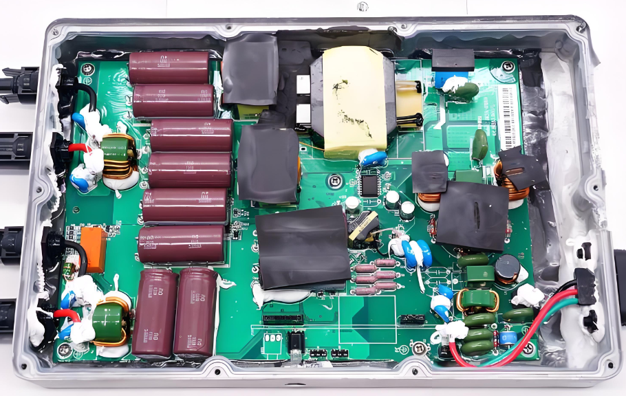
Motor Control PCB technology serves as the intelligent interface between command signals and physical motion, translating digital instructions into precise electrical currents that drive motors with exceptional accuracy and efficiency. These sophisticated circuit boards form the operational core of modern motion systems, balancing power delivery, thermal management, and signal integrity within increasingly compact form factors. This comprehensive guide explores the engineering principles, design methodologies, and practical implementation strategies that define advanced motor control PCB solutions, providing engineers and system designers with actionable insights for next-generation motion system development.
Are you struggling with motor control implementations that fail to deliver expected performance, reliability, or efficiency? Engineers developing motion systems consistently face several critical challenges:
Thermal Management Difficulties: High-current operation generates excessive heat, leading to premature component failure and reduced lifespan without proper dissipation strategies.
Electromagnetic Interference Issues: Switching noise from PWM signals disrupts sensitive control circuits, compromising precision in demanding applications.
Space Constraints vs. Power Requirements: Shrinking form factors conflict with increasing power densities, creating engineering trade-offs that impact overall system performance.
Signal Integrity Degradation: Mixed-signal environments where high-power switching noise corrupts low-voltage control signals, reducing positioning accuracy and control stability.
Complex Implementation Barriers: Sophisticated control algorithms like FOC require specialized expertise and careful PCB layout, increasing development time and cost.
Modern motor control PCB technologies address these challenges through innovative engineering approaches:
Advanced Thermal Management Architectures: Implementing thermal vias, copper pours, and strategic component placement to dissipate heat effectively, ensuring reliability under demanding operating conditions.
Comprehensive EMI Reduction Techniques: Careful grounding strategies, component separation, and filtering methods that minimize electromagnetic interference, preserving signal integrity in noisy environments.
High-Density Power Delivery Systems: Utilizing multilayer boards with dedicated power planes and optimized trace geometries to deliver substantial current within minimal board area.
Mixed-Signal Layout Optimization: Implementing separation techniques and guard traces to isolate sensitive control signals from power switching noise, maintaining precision in challenging environments.
Integrated Development Ecosystems: Combining hardware reference designs with software libraries and configuration tools that streamline implementation of advanced control methodologies.
At BEST Technology, we specialize in manufacturing advanced motor control PCBs that overcome these challenges through innovative engineering and precision manufacturing. Our expertise spans from basic DC motor controllers to complex multi-axis motion systems, ensuring optimal performance for your specific application requirements. For more information or if you would like to send us any inquiry, please send us an email through the contact form at the bottom of our Contact US Page.
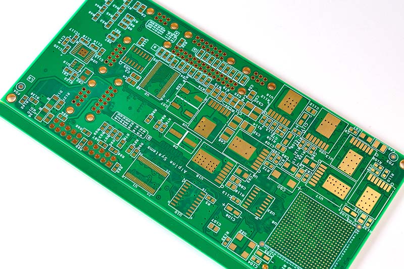
What Is a Motor Control PCB?
A motor control PCB is a specialized printed circuit board designed specifically to manage the electrical power delivered to an electric motor, translating command signals into precise motion output. These intelligent boards serve as the critical interface between low-power control systems (such as microcontrollers or processors) and the high-power demands of motors, enabling sophisticated control over speed, torque, position, and operational characteristics.
Unlike generic circuit boards, motor control PCBs incorporate several distinctive elements that make them uniquely suited for their role. They typically feature power transistors or MOSFETs capable of handling substantial currents, gate driver circuits for switching control, current sensing mechanisms for feedback, and protection circuits to prevent damage from overcurrent, overvoltage, or thermal overload conditions. The specific component selection and layout vary significantly depending on whether the board is designed for DC, stepper, or brushless DC (BLDC motor controller PCB) applications.
The fundamental importance of motor control PCBs in modern motion systems cannot be overstated. They enable the precision control necessary for applications ranging from delicate robotic surgery instruments to powerful industrial automation equipment. By implementing sophisticated control algorithms like Field-Oriented Control (FOC) and Space Vector PWM (SVPWM), these PCBs deliver smooth, efficient motor operation across speed and torque ranges that were previously unattainable with simpler control methods.
Table: Comparison of Motor Control PCB Types
PCB Type
Typical Applications
Key Characteristics
Control Methodology
DC Motor Controller PCB
Toys, Pumps, Small Devices
H-bridge, PWM Control
Voltage & Direction
Stepper Motor Driver PCB
3D Printers, CNC, Robotics
Microstepping, Phasing
Pulses & Current
BLDC Motor Controller PCB
Drones, EVs, Tools
3-phase Bridge, Sensors
Commutation, FOC
PCB Stator Motor Controller
Robotics, Aerospace, Medical
Thin Design, High Precision
Digital & Adaptive
The evolution of motor control circuit board PCB board technology continues to push the boundaries of what’s possible in motion control, with recent advancements incorporating wide-bandgap semiconductors (SiC and GaN), integrated motor-driver solutions, and advanced thermal management techniques that collectively enhance power density, efficiency, and reliability.
How Does a Motor Control Board Work?
A motor control board operates through a sophisticated interplay of power regulation, signal processing, and feedback mechanisms that collectively transform command signals into precise motor motion. At its core, the board functions as a translator and amplifier, converting low-power signals from a microcontroller or command source into the high-current, high-voltage signals necessary to drive motors effectively. This process involves multiple stages of signal conditioning, power switching, and real-time monitoring to ensure accurate and reliable operation.
The operational sequence begins when the board receives a command signal indicating the desired motor behavior (speed, position, or torque). This signal is processed by control logic, which determines the appropriate switching sequence for the power stage. The power stage then delivers energy to the motor windings in a carefully controlled manner, while feedback sensors continuously monitor actual motor performance. This feedback allows the control logic to make real-time adjustments, creating a closed-loop system that maintains the desired output despite variations in load or operating conditions.
Critical Components and Their Functions
Understanding the individual components that comprise a motor control board reveals how these systems achieve such precise control over electric motors:
Microcontroller/Processor: Serves as the intelligent core of the system, executing control algorithms (PID, FOC, etc.) and making real-time decisions based on sensor feedback and command inputs. Modern motor control boards often feature powerful 32-bit ARM Cortex-M processors capable of running advanced algorithms at high speeds.
Gate Driver Circuits: Amplify low-power signals from the microcontroller to voltage and current levels sufficient to drive the power switches efficiently. These circuits ensure rapid switching of MOSFETs or IGBTs while providing necessary isolation and protection features.
Power Switches (MOSFETs/IGBTs): Function as electronic valves that control power flow to the motor windings. The specific configuration (H-bridge for DC motors, three-phase bridge for BLDC motors) determines how the motor operates in terms of direction, speed, and torque generation.
Current Sensing Circuits: Monitor electrical current flowing to the motor using shunt resistors, Hall effect sensors, or current transformers. This information is crucial for torque control and protection functions, enabling the implementation of advanced control strategies like Field-Oriented Control.
Protection Circuits: Include overcurrent detection, overvoltage clamping, thermal monitoring, and undervoltage lockout mechanisms that safeguard both the control board and the motor from damage under fault conditions.
Control Methodologies and Signal Processing
Different motor types require distinct control approaches, which the motor control board implements through specialized circuitry and algorithms:
For DC motor speed control PCB applications, Pulse Width Modulation (PWM) is the predominant control strategy. The board varies the duty cycle of switching signals to effectively control the average voltage applied to the motor, thereby regulating speed. An H-bridge configuration enables bidirectional current flow, permitting both forward and reverse operation.
In brushless DC motor controller PCB systems, the control board must sequentially energize the motor phases in synchronization with rotor position. This requires either sensor-based feedback (from Hall effect sensors or encoders) or sensorless techniques that monitor back-EMF to determine commutation timing. Advanced boards implement Field-Oriented Control, which decouples torque and flux-producing currents for superior efficiency and dynamic response.
Stepper motor controllers employ a different approach, sending precise pulse sequences to advance the motor in discrete steps. Microstepping techniques subdivide these steps for smoother operation and reduced resonance, requiring sophisticated current control through each motor winding.
Table: Motor Control Board Signal Processing Stages
Processing Stage
Function
Key Components
Command Input
Receives control signals
UART / SPI / CAN
Signal Conditioning
Filters input signals
Op-amps, RC parts
Control Algorithm
Computes motor output
MCU / DSP
PWM Generation
Creates timing pulses
PWM timers
Gate Driving
Drives power switches
Gate drivers
Feedback Acquisition
Reads motor feedback
ADCs, sensors
The sophistication of modern motor control PCB board designs continues to evolve, with integrated solutions like Texas Instruments’ MCF8316C and MCF8315C devices combining control algorithms, gate drivers, and power stages into single-chip solutions that reduce design complexity while enhancing performance and reliability.
How Does a BLDC Motor Controller PCB Achieve Smooth and Precise Motor Operation?
A brushless DC motor controller PCB achieves exceptional smoothness and precision through sophisticated control algorithms that optimize performance across the entire operating range. The most significant advancement in BLDC control methodology is Field-Oriented Control (FOC), a technique that decouples the control of torque-producing and magnetic flux-producing components of motor current. This approach enables seamless operation similar to high-performance DC motors but with the efficiency benefits of brushless technology.
The FOC algorithm implementation on a BLDC motor controller PCB involves several computational stages. First, the controller measures two motor phase currents, deriving the third using Kirchhoff’s law. These measurements are transformed from a three-phase system to a two-axis rotating reference frame using the Clarke and Park transformations. This mathematical manipulation allows the controller to independently manage torque (q-axis) and flux (d-axis) components. After applying appropriate control strategies (typically PID controllers), the algorithm transforms the signals back to the three-phase domain for PWM generation.
Critical Sensor Integration and Feedback Mechanisms
Precision operation in BLDC motors relies heavily on accurate feedback systems integrated into the motor control PCB. Two primary sensing approaches dominate modern implementations:
Sensor-based systems utilize Hall effect sensors or encoders mounted within the motor to provide precise rotor position information. These sensors deliver digital or analog signals to the controller, enabling exact commutation timing. Encoders, especially absolute and multi-turn variants, offer the highest position resolution, making them ideal for applications requiring precise positioning such as robotic arms and CNC machines.
Sensorless control techniques have gained significant popularity for their reduced component count and cost advantages. These methods typically monitor the back-electromotive force (back-EMF) generated in the unenergized motor winding during operation. As the motor rotates, each winding generates a voltage proportional to speed, with zero-crossing points indicating commutation events. Advanced sensorless algorithms can achieve performance comparable to sensored systems, particularly at medium to high speeds.
PWM Techniques and Switching Optimization
The quality of BLDC motor operation heavily depends on the pulse-width modulation techniques employed by the controller PCB. Standard PWM methods have evolved to include sophisticated approaches that optimize switching patterns for reduced acoustic noise, improved efficiency, and smoother torque production:
Sinusoidal PWM: Provides smooth sinusoidal current to the motor windings, reducing torque ripple and acoustic noise compared to traditional six-step commutation.
Space Vector PWM (SVPWM): A more advanced technique that offers approximately 15% better DC bus utilization compared to sinusoidal PWM, resulting in higher torque output capabilities without increasing voltage requirements.
Advanced Modulation Schemes: Techniques such as discontinuous PWM and third-harmonic injection further optimize switching losses and electromagnetic performance, particularly important in high-frequency applications.
The switching frequency selection represents a critical design trade-off. Higher frequencies (typically 20-100 kHz) move acoustic noise above the human hearing range and reduce current ripple but increase switching losses. Lower frequencies improve efficiency but may produce audible noise and require larger filtering components.
Implementation Considerations for Smooth Operation
Achieving truly smooth BLDC operation requires attention to several implementation details on the motor controller PCB:
Current Sensing Accuracy is paramount for precise torque control. High-quality sampling circuits with adequate resolution (typically 12-16 bits), proper filtering, and careful layout ensure accurate current measurements. Multiple sampling techniques including low-side, high-side, and inline resistor configurations each offer distinct advantages for different applications.
Dead Time Insertion prevents shoot-through currents that can damage power switches during phase transitions. However, improper dead time compensation introduces distortion, so modern controllers implement adaptive compensation techniques that maintain waveform integrity while ensuring safety.
Startup and Low-Speed Optimization presents particular challenges, especially for sensorless designs that rely on back-EMF measurement. Advanced startup sequences typically begin with rotor alignment followed by open-loop acceleration until sufficient back-EMF develops for transition to closed-loop operation. Sophisticated algorithms smoothly manage this transition to prevent stalling or hesitation.
The integration of these techniques in modern BLDC motor controller PCB designs enables remarkable performance characteristics, with efficiency levels exceeding 90% and torque ripple reduced to less than 2% in optimized implementations.
What Design Principles Ensure a Stable and Efficient Motor Driver PCB and Motor Controller PCB Layout?
The foundation of a stable motor driver PCB begins with strategic component placement that segregates circuits based on their signal characteristics and power requirements. Effective partitioning separates high-power switching sections (containing MOSFETs/IGBTs and gate drivers) from sensitive analog and digital control circuits, minimizing noise coupling and ensuring signal integrity.
A well-designed motor controller PCB layout follows a logical flow from power input to motor output, with components arranged to minimize current path lengths and loop areas. The power stage components should be clustered together, with gate drivers positioned immediately adjacent to their corresponding power switches to keep gate drive traces short (typically <15mm). This placement strategy reduces parasitic inductance that can cause voltage spikes and switching artifacts.
Critical to this partitioning approach is the establishment of distinct functional zones:
Power Input Section: Where bulk capacitors and filtering components are located near power connectors
Switching Power Stage: Containing MOSFETs/IGBTs and gate drivers in a compact arrangement
Control Section: Housing the microcontroller and support components in a quiet area of the board
Feedback Circuits: Positioning current sensors and analog conditioning circuits away from noise sources
Communication Interfaces: Isolating sensitive digital interfaces from power switching noise
Power Delivery System Design
A robust power delivery system is essential for motor driver PCB stability and efficiency. This begins with appropriate PCB layer stackup design, where multi-layer boards (typically 4-6 layers) provide dedicated power and ground planes that offer low-impedance current paths and excellent noise suppression.
The power delivery network must be designed to handle both continuous and peak current demands without excessive voltage drop or heating. Trace width calculations based on current requirements are critical, with external layers capable of carrying approximately 30-50% more current than internal traces of the same width due to better heat dissipation. For high-current applications (typically >5A), 2oz or heavier copper is recommended to reduce resistance and improve current-handling capability.
Table: PCB Trace Width Recommendations for Motor Control Applications
Current (A)
1oz Copper (10°C rise)
2oz Copper (10°C rise)
1oz Copper (20°C rise)
2oz Copper (20°C rise)
5A
1.2mm (47 mil)
0.6mm (24 mil)
0.8mm (31 mil)
0.4mm (16 mil)
10A
3.0mm (118 mil)
1.5mm (59 mil)
2.0mm (79 mil)
1.0mm (39 mil)
20A
8.5mm (335 mil)
4.2mm (165 mil)
5.5mm (217 mil)
2.8mm (110 mil)
30A
15.0mm (591 mil)
7.5mm (295 mil)
10.0mm (394 mil)
5.0mm (197 mil)
Decoupling capacitor placement significantly impacts high-frequency performance. Small ceramic capacitors (100nF-1μF) should be located as close as possible to IC power pins, with larger bulk capacitors (10-100μF) distributed throughout the board to maintain stable voltage during transient loads.
Thermal Management Strategies
Effective thermal management is non-negotiable for reliable motor control PCB operation. Power dissipation in switching components and current-carrying traces generates heat that must be efficiently conducted away from critical components to prevent thermal runaway and ensure long-term reliability.
Several techniques contribute to optimal thermal performance:
Thermal Via Arrays: Placing multiple vias (typically 0.3-0.5mm diameter) beneath power component thermal pads conducts heat to inner and opposite copper layers, significantly improving heat dissipation. These vias should be filled with thermal epoxy or solder for optimal thermal transfer.
Copper Pour Utilization: Large copper areas connected to power components act as heat spreaders, increasing surface area for convective cooling. The effectiveness of these pours depends on their size, connection method, and exposure to airflow.
Component Placement Considerations: Distributing heat-generating components across the board prevents localized hot spots. When high-power components must be clustered, additional cooling measures such as heatsinks or forced airflow are necessary.
Thermal Interface Materials: Selecting appropriate thermal compounds, pads, or phase-change materials between components and heatsinks minimizes thermal resistance, improving heat transfer efficiency.
For applications with extreme power demands, metal-core PCBs (MCPCB) provide superior thermal conductivity compared to standard FR-4 substrates, though at increased cost and manufacturing complexity.
Grounding and EMI Control Techniques
Proper grounding strategies form the foundation of EMI control in motor driver PCB designs. A single, continuous ground plane is generally preferred over multiple segmented grounds, as it provides a low-impedance return path and minimizes ground bounce.
When dealing with mixed-signal designs containing analog, digital, and power sections, the ground plane separation approach must be carefully considered. While complete separation seems intuitively correct, it can create more problems than it solves by forcing return currents to take longer paths, increasing loop areas and EMI radiation. A better approach maintains a unified ground plane with careful component placement to prevent noise coupling.
Additional EMI reduction techniques include:
Guard Traces: Placing grounded copper barriers between noisy and sensitive circuits provides additional isolation.
Filtering Networks: Implementing RC filters on sensitive analog inputs and motor feedback signals suppresses high-frequency noise.
Proper Shielding: Using shielded cables for external connections and incorporating shielded compartments for particularly sensitive circuits.
Slowing Switching Edges: Adding small resistors (2-10Ω) in series with gate drive paths reduces dv/dt, decreasing EMI generation at the cost of slightly increased switching losses.
By implementing these design principles, motor controller PCB layout can achieve the stability and efficiency required for demanding motion control applications, ensuring reliable operation across diverse operating conditions.
How Does a DC Motor Speed Control PCB Regulate Speed, Torque, and Power Output?
The primary method employed by a DC motor speed control PCB to regulate motor velocity is Pulse Width Modulation (PWM), a technique that varies the average voltage applied to the motor by switching power to the load at a high frequency with adjustable duty cycles. Rather than delivering a variable analog voltage, the controller rapidly switches full power on and off, with the proportion of on-time to off-time (duty cycle) determining the effective voltage seen by the motor.
The PWM frequency selection represents a critical design decision that balances several factors. Lower frequencies (typically 1-5 kHz) are more efficient with lower switching losses but may produce audible noise and result in larger current ripple. Higher frequencies (20-50 kHz) move the switching noise above the audible range and reduce current ripple but increase switching losses in the power devices. Modern DC motor controller PCB designs typically operate in the 15-25 kHz range, optimizing both acoustic performance and efficiency.
The implementation of PWM control involves an H-bridge configuration comprising four power switches (usually MOSFETs) arranged in a bridge configuration. This arrangement allows bidirectional current flow through the motor, enabling both forward and reverse operation. By controlling the switching sequence of these four devices, the controller can apply positive voltage, negative voltage, or brake the motor by shorting its terminals.
Torque Control and Current Regulation
Beyond basic speed control, advanced DC motor speed control PCB designs implement precise torque regulation through current control techniques. Since motor torque is directly proportional to armature current, measuring and controlling current enables accurate torque management essential for applications like robotic arms, conveyor systems, and precision tools.
Current sensing typically employs one of several methods:
Shunt Resistors: Low-value, high-precision resistors placed in series with the motor current path, with the voltage drop across the resistor proportional to current. This method offers excellent accuracy and bandwidth but introduces power losses.
Hall Effect Sensors: Magnetic field sensors that measure current without direct electrical connection, providing isolation and minimal insertion loss. These are preferred for higher-current applications but are more expensive and may have limited bandwidth.
Current Transformer: Used for AC current measurement, these provide inherent isolation but are unsuitable for DC measurement without additional circuitry.
Once measured, the current feedback is compared to a torque command, with the error processed by a PI controller that adjusts the PWM duty cycle to maintain the desired current level. This closed-loop current control enables precise torque regulation even as motor back-EMF varies with speed.
Power Output Optimization and Efficiency Considerations
Efficient power delivery is a hallmark of well-designed DC motor controller PCB systems. Several techniques contribute to optimized power output:
Synchronous Rectification significantly improves efficiency in PWM motor drives. During the off-time of the PWM cycle, the motor’s inductance causes current to continue flowing through the body diodes of the MOSFETs. By intentionally turning on the appropriate MOSFETs during this period (synchronous conduction), the voltage drop reduces from approximately 0.7V (diode forward voltage) to just the MOSFET’s RDS(ON) voltage drop, typically 0.05-0.10V for modern devices. This reduction in voltage drop decreases power losses, particularly at light loads where conduction time is short.
Dead Time Management addresses a potential issue in H-bridge operation. To prevent shoot-through currents (both high-side and low-side switches on simultaneously), a small dead time is inserted between turning one switch off and turning the complementary switch on. However, improper dead time causes distortion at zero-current crossings and reduces effective voltage. Advanced controllers implement adaptive dead time compensation to minimize these effects.
Supply Voltage Compensation maintains consistent performance across varying input voltages. As battery voltage declines in portable applications or line voltage fluctuates in stationary systems, the PWM duty cycle requires adjustment to maintain the same effective motor voltage. Sophisticated controllers incorporate input voltage monitoring and automatic compensation.
Advanced Control Algorithms for Enhanced Performance
While basic PWM control suffices for many applications, advanced DC motor speed control PCB implementations employ sophisticated algorithms for superior performance:
PID Speed Control combines proportional, integral, and derivative terms to achieve precise speed regulation. The proportional term responds to immediate error, the integral term eliminates steady-state error, and the derivative term improves response to changing loads. Carefully tuned PID controllers maintain consistent speed despite varying mechanical loads.
Adaptive Control techniques automatically adjust control parameters as operating conditions change. For example, the controller might recognize that higher torque levels require different gain settings to maintain stability, or that motor characteristics change with temperature, necessitating corresponding adjustments to the control strategy.
Field-Weakening Control extends the speed range beyond the motor’s base speed. In permanent magnet DC motors, back-EMF limits the maximum speed at which the motor can be driven with available voltage. By intentionally reducing the magnetic flux (in wound-field motors) or applying advanced current phase control (in BLDC motors), the controller can achieve higher speeds at the expense of reduced torque capability.
These advanced control techniques, implemented through sophisticated motor control PCB programming, enable DC motor controllers to deliver precise, efficient, and responsive performance across a wide range of operating conditions and application requirements.
What Makes PCB Stator Motor Technology Unique and How Does It Expand PCB Motor Application?
PCB Stator motor technology represents a revolutionary approach to electric motor design that replaces traditional copper wire windings with precision-etched printed circuit boards as the stator component. This innovative methodology leverages printed circuit board manufacturing techniques to create intricate, multilayer stator structures that offer significant advantages over conventional motor construction.
The core innovation lies in the replacement of hand-wound or machine-wound copper coils with photolithographically defined traces on a rigid or flexible PCB substrate. These traces form the motor windings with exceptional precision and consistency, eliminating the variations and imperfections inherent in traditional winding processes. The resulting stator is dramatically thinner and lighter than conventional designs while maintaining excellent electromagnetic performance.
A key differentiator of PCB Stator motor technology is its integration of the motor drive and control electronics directly onto the stator PCB itself. This integration creates a compact, unified system that reduces the overall footprint and eliminates many of the interconnects that can introduce reliability issues in traditional motor systems. The approach enables unprecedented levels of miniaturization while maintaining high power density.
Performance Advantages and Technical Superiority
The unique characteristics of PCB Stator motor design translate into several compelling performance advantages that expand potential applications:
Exceptional Power Density is perhaps the most significant benefit, with PCB stator motors delivering up to 70% weight reduction and 50% size reduction compared to conventional motors of equivalent power output. This dramatic improvement stems from the elimination of bulky copper windings and the integration of control electronics within the motor structure itself.
Superior Efficiency results from the precise control over trace geometry and the ability to optimize the winding pattern for specific operating conditions. PCB stator motors achieve efficiencies exceeding 90% across a broad operating range, with some implementations reaching 95% efficiency in targeted applications. This efficiency advantage translates to reduced energy consumption and less waste heat generation.
Acoustic Performance improvements are another notable benefit. The absence of cogging torque (due to the slotless design) and the precision of the magnetic circuit result in exceptionally quiet operation with near-zero acoustic signature. This characteristic makes PCB stator motors ideal for applications where noise is a critical concern.
Thermal Management advantages arise from the distributed nature of the windings across the PCB substrate, which provides a large surface area for heat dissipation. Additionally, the integration of thermal vias and the ability to incorporate heatsinking directly into the PCB structure enable effective cooling in high-power-density applications.
Expanded Application Horizons
The unique properties of PCB Stator motor technology open up new application possibilities that were previously challenging or impossible with conventional motor technologies:
Aerospace and Aviation applications benefit tremendously from the weight reduction and compact form factors. Drones, electric aircraft, and satellite systems can achieve significant performance improvements through the integration of PCB stator motors, where every gram of weight reduction translates to extended flight time or increased payload capacity.
Medical Devices represent another promising application area, where the combination of compact size, quiet operation, and precision control aligns perfectly with requirements for surgical robots, diagnostic equipment, and portable medical devices. The ability to create custom motor geometries enables integration into space-constrained medical instruments.
Robotics and Automation systems gain advantages from the high torque density and precise control capabilities of PCB stator motors. Collaborative robots, in particular, benefit from the compact dimensions and excellent torque responsiveness, enabling more natural and safer human-robot interaction.
Consumer Electronics and Internet of Things (IoT) devices represent emerging application areas where the small form factor, quiet operation, and efficiency of PCB stator motors enable new product categories and enhanced functionality in existing products.
Integration with Advanced Control Systems
The PCB Stator motor design naturally complements advanced control methodologies, particularly when integrated with sophisticated motor control PCB electronics. The precise, predictable electromagnetic characteristics of PCB stators enable implementation of advanced control algorithms with exceptional accuracy.
ECM’s “Eight Ball” servo motor exemplifies this integration, combining a 50:1 harmonic drive with a PCB stator motor and dual encoder feedback system. This configuration delivers remarkable performance characteristics: 33.9 Nm peak torque and 18.8 Nm continuous torque in a package weighing just 0.57 kg with dimensions of 2.95″ × 3.35″ × 1.96″. Such performance would be difficult or impossible to achieve with conventional motor technologies.
The PrintStator Motor CAD platform further enhances the capabilities of PCB stator technology by enabling digital motor design and optimization. This software-driven approach allows engineers to create custom motor solutions tailored to specific application requirements, significantly reducing development time and cost while optimizing performance.
As PCB Stator motor technology continues to evolve, it promises to redefine the possibilities for electric motion systems across an expanding range of industries and applications, offering unprecedented combinations of performance, efficiency, and compactness.
How Do OEM Motor Control Circuit Board PCB Board Manufacturers Guarantee Reliability and Quality?
OEM motor control circuit board PCB board manufacturers implement rigorous design validation processes to ensure reliability before production begins. These processes involve simulation and modeling of electrical, thermal, and mechanical performance under various operating conditions. Advanced software tools simulate power integrity, signal integrity, and thermal behavior, identifying potential issues early in the design phase when corrections are most cost-effective.
A key aspect of design validation is Design for Manufacturability (DFM) analysis, which identifies potential production issues before tooling begins. DFM checks ensure that the PCB design complies with manufacturing capabilities regarding minimum trace widths, spacing, hole sizes, and other geometric constraints. Similarly, Design for Assembly (DFA) analysis optimizes component placement and orientation for efficient, reliable assembly, considering factors such as solder joint quality, thermal management during reflow, and accessibility for automated testing.
Design for Testability (DFT) represents another critical validation aspect, incorporating test points, boundary scan capabilities, and other features that facilitate comprehensive testing during manufacturing. These features enable manufacturers to verify proper component operation and interconnection before the board reaches customers, catching defects early in the production process.
Advanced Manufacturing Techniques and Quality Control
The manufacturing process for motor control circuit board PCB board products incorporates multiple quality assurance checkpoints to maintain consistent quality:
Material Selection forms the foundation of reliability. High-temperature FR-4 substrates with appropriate Tg (glass transition temperature) values are essential for motor control applications where components may operate at elevated temperatures. For high-power applications, manufacturers often recommend heavy copper PCBs (2-6 oz) to handle high currents without excessive heating.
Precision Fabrication processes ensure dimensional accuracy and consistency. Laser direct imaging (LDI) systems achieve finer trace geometries than traditional photolithography, while automated optical inspection (AOI) systems verify critical dimensions and detect defects such as shorts, opens, or insufficient spacing.
Component Sourcing and Verification plays a crucial role in reliability. Established manufacturers maintain relationships with authorized distributors of reputable components, avoiding counterfeit parts that plague the electronics industry. Incoming components undergo verification testing, particularly for critical components such as power semiconductors that directly impact product reliability.
Table: Quality Control Checkpoints in Motor Control PCB Manufacturing
Reliability assurance continues with rigorous testing protocols that evaluate motor control PCB performance under simulated operating conditions:
In-Circuit Testing (ICT) verifies the presence, orientation, and value of components, while also checking for shorts and opens in the circuitry. Fixture-based ICT systems make contact with test points throughout the board, providing comprehensive electrical verification.
Functional Testing subjects the completed motor control board to simulated operating conditions, applying power and control signals while monitoring outputs. This testing validates that the board performs its intended functions correctly, including proper motor driving, feedback sensing, and protection features.
Environmental Stress Screening exposes boards to accelerated aging conditions such as thermal cycling, vibration, and humidity. Highly reliable applications may require Highly Accelerated Life Testing (HALT) or Highly Accelerated Stress Screening (HASS) to identify potential failure mechanisms and verify robustness.
Burn-in Testing operates boards at elevated temperatures and voltages for extended periods to identify infant mortality failures before products ship to customers. This process is particularly important for applications where reliability is critical, such as automotive, medical, or industrial systems.
Reliability Certification and Continuous Improvement
Reputable OEM motor control circuit board PCB board manufacturers maintain certifications that demonstrate their commitment to quality and reliability. ISO 9001 quality management system certification ensures consistent processes and continuous improvement, while IATF 16949 is essential for automotive applications. Specific industry certifications such as ISO 13485 for medical devices or AS9100 for aerospace applications may be required for specialized markets.
Failure Analysis capabilities complement these certifications, enabling manufacturers to investigate any field returns or test failures to determine root causes and implement corrective actions. This closed-loop process drives continuous improvement in both design and manufacturing, enhancing reliability over successive product generations.
By implementing these comprehensive approaches to reliability and quality, reputable manufacturers deliver motor control PCBs that meet the demanding requirements of modern motion control applications, ensuring long-term performance and customer satisfaction.
How Does Motor Control PCB Programming Optimize 12V and High-Power Motor Systems?
Motor control PCB programming creates the intelligent layer that optimizes performance across varying voltage domains, from compact 12V systems to high-power industrial applications. The firmware architecture typically implements a modular structure that separates hardware abstraction, control algorithms, and application logic, enabling code reuse across different motor platforms while maintaining optimization for specific operating conditions.
For 12V motor control PCB applications, typically found in automotive, robotics, and consumer products, programming focuses on efficiency optimization due to often limited power availability. These implementations emphasize low quiescent current, sleep modes, and efficient startup sequences to minimize power consumption during idle periods. The code manages trade-offs between performance and battery life, implementing adaptive algorithms that adjust behavior based on available voltage and load conditions.
High-power systems, in contrast, prioritize thermal management and protection mechanisms in their programming. Firmware for these applications incorporates comprehensive monitoring of temperature, current, and voltage parameters, dynamically adjusting operation to prevent damage under fault conditions. Advanced implementations may include model predictive control algorithms that anticipate thermal behavior and adjust control parameters preemptively to maintain safe operating temperatures.
Advanced Control Algorithm Implementation
The sophistication of modern motor control PCB programming enables implementation of advanced algorithms that optimize performance across diverse operating conditions:
Field-Oriented Control (FOC) represents the gold standard for brushless motor control, particularly in high-performance applications. This algorithm decouples the control of magnetic flux and torque-producing current components, enabling seamless operation similar to separately excited DC motors. FOC implementation requires substantial computational resources, typically running on 32-bit ARM Cortex-M processors with hardware acceleration for mathematical transformations.
Sensorless Control Techniques eliminate the need for physical position sensors, reducing cost and improving reliability. These algorithms estimate rotor position by monitoring back-EMF in undriven motor phases, with sophisticated variants incorporating High-Frequency Injection for position estimation at standstill and low speeds. The programming must seamlessly transition between different estimation techniques as speed increases, maintaining stability across the entire operating range.
Adaptive PID Tuning addresses the challenge of maintaining optimal control performance as motor characteristics change with operating conditions. Rather than using fixed PID gains, adaptive implementations continuously adjust proportional, integral, and derivative parameters based on observed performance. Some advanced systems implement self-tuning algorithms that automatically determine optimal PID parameters during commissioning or operation.
Performance Optimization Strategies
Motor control PCB programming implements various strategies to optimize specific aspects of motor performance:
Efficiency Optimization focuses on minimizing losses across the operating range. Techniques include phase advance optimization for brushless motors, which adjusts the timing of commutation events to maximize torque per amp, particularly at high speeds. Maximum Torque Per Ampere (MTPA) algorithms continuously optimize current angle to achieve the highest possible efficiency for a given torque output.
Acoustic Noise Reduction is critical for applications where silent operation is important. Programming techniques include PWM frequency modulation to spread acoustic energy across a broader frequency spectrum, reducing perceptible noise. Smooth commutation transitions through sinusoidal drive or advanced modulation schemes also minimize audible vibration caused by torque ripple.
Torque Ripple Minimization enhances smoothness, particularly at low speeds where ripple is most noticeable. Advanced implementations employ iterative learning control or repetitive control techniques that identify periodic disturbances in the torque output and generate compensating signals to cancel them.
Protection and Diagnostic Features
Comprehensive protection mechanisms are essential components of motor control PCB programming, particularly for high-power systems where faults can have serious consequences:
Real-Time Fault Detection algorithms monitor current, voltage, temperature, and position signals continuously, comparing them against predefined thresholds. When anomalies are detected, the firmware initiates appropriate responses, ranging from controlled shutdowns to graceful performance reduction, depending on the severity of the fault.
Predictive Maintenance capabilities represent an advanced feature in modern motor controllers. By tracking operating hours, temperature profiles, and load cycles, the firmware can estimate component aging and predict potential failures before they occur. This information enables proactive maintenance, reducing downtime in critical applications.
Commissioning and Diagnostics routines simplify setup and troubleshooting. Automated commissioning sequences characterize motor parameters upon initial installation, determining electrical and mechanical properties that optimize control parameters. Comprehensive diagnostic capabilities provide detailed information about system status and historical performance, facilitating troubleshooting and reducing mean time to repair.
Through these sophisticated programming approaches, modern motor control PCBs deliver optimized performance across diverse applications, from precision 12V systems to high-power industrial drives, maximizing efficiency, reliability, and functionality.
How to Test a Motor Control Circuit?
Testing a motor control circuit requires a systematic approach that progresses from basic validation to comprehensive performance characterization under simulated operating conditions. A well-structured testing regimen ensures reliability, safety, and performance compliance with design specifications.
The testing process typically begins with static measurements without power applied, progresses to power-on functional verification, and culminates in dynamic performance testing under load. At each stage, specific parameters are measured and compared against expected values, with deviations triggering investigation and corrective action.
Essential Test Equipment and Setup
Proper test equipment selection is crucial for accurate motor control circuit evaluation:
Oscilloscope: A minimum 100MHz bandwidth digital oscilloscope with multiple channels is essential for observing PWM signals, current waveforms, and timing relationships. High-voltage differential probes are necessary for safely measuring switching waveforms in high-voltage circuits.
Programmable Power Supply: A DC power supply capable of delivering the expected voltage and current ranges while providing measurement readbacks enables controlled power application during testing.
Electronic Load or Dynamometer: For testing under realistic load conditions, an electronic load or mechanical dynamometer applies controllable torque to the motor, allowing performance characterization across the operating range.
Current Probes: High-bandwidth current probes (Hall effect or Rogowski coil) accurately capture motor phase currents without introducing significant resistance or disturbing the circuit.
Thermal Measurement Equipment: Infrared thermometers or thermal cameras provide non-contact temperature measurements of critical components during operation.
Data Acquisition System: For comprehensive testing, a multi-channel DAQ system records voltage, current, temperature, and speed measurements simultaneously, enabling detailed performance analysis.
Step-by-Step Testing Procedure
A methodical approach to motor control circuit testing ensures thorough validation:
1. Visual Inspection and Continuity Testing
Before applying power, conduct a thorough visual examination of the PCB for manufacturing defects such as solder bridges, missing components, or physical damage. Follow with continuity testing to verify proper connections and absence of shorts, particularly between power rails and ground.
2. Power-Up and Quiescent Current Measurement
Apply low voltage (e.g., 5V) to the control circuitry first, measuring quiescent current to detect potential short circuits. Gradually increase voltage to nominal levels while monitoring current draw, ensuring values align with expectations based on the design.
3. Control Signal Verification
With power applied but motor disconnected, verify proper operation of control interfaces. Apply command signals (PWM, analog voltage, or digital commands) and observe the resulting gate drive signals using an oscilloscope. Check for correct timing, amplitude, and waveform characteristics.
4. Gate Drive Signal Analysis
Examine gate drive waveforms for proper shape, rise/fall times, and absence of ringing or oscillations. Excessive ringing indicates layout issues or inadequate gate resistance. Verify that dead time insertion prevents shoot-through in bridge configurations.
5. No-Load Motor Testing
Connect the motor without mechanical load and apply gradually increasing commands. Monitor motor acceleration, listening for unusual noises and observing current draw. For BLDC motors, verify smooth rotation throughout the speed range, particularly during startup.
6. Protection Circuit Validation
Test each protection feature individually:
Overcurrent Protection: Momentarily apply excessive load or simulate overcurrent condition to verify shutdown response
Overvoltage/Undervoltage Protection: Vary supply voltage to trigger protection circuits
Thermal Protection: Use a heat gun or similar to raise component temperatures while monitoring protection response
7. Dynamic Performance Characterization
Under controlled load conditions, measure:
Efficiency: Power input versus mechanical power output across speed and torque range
Speed Regulation: Ability to maintain set speed under varying loads
Torque Response: Step changes in torque demand and response characteristics
Thermal Performance: Temperature rise of critical components during continuous operation
Table: Motor Control Circuit Performance Metrics and Test Conditions
Performance Metric
Test Condition
Acceptance Criteria
Startup Reliability
Multiple start-stop cycles at various positions
Smooth rotation without hesitation
Speed Regulation
±50% load variation at constant speed command
<2% speed deviation
Efficiency
25%, 50%, 75%, 100% of rated load
>85% (varies by motor type and power)
Thermal Stability
2 hours at rated load
Temperature stabilization below maximum ratings
Audible Noise
Entire speed range at light load
<45 dBA at 1 meter distance
Advanced Testing Techniques
For comprehensive validation, several advanced testing approaches provide deeper insights:
Loop Response Analysis characterizes the control system’s stability and response characteristics. Using a frequency response analyzer or specialized software, inject a small signal perturbation into the control loop and measure the system’s response. This analysis verifies phase and gain margins, ensuring stable operation under all conditions.
EMI/EMC Pre-compliance Testing identifies potential electromagnetic interference issues before formal certification testing. Using a spectrum analyzer with near-field probes, scan the operating circuit for emissions hotspots. This preliminary testing allows design modifications before costly formal testing.
Accelerated Life Testing subjects the motor control circuit to elevated stress levels (temperature, voltage, vibration) to identify potential failure mechanisms and estimate product lifetime under normal operating conditions. While requiring specialized equipment, this testing provides valuable reliability data.
By following this comprehensive testing methodology, engineers can thoroughly validate motor control circuit performance, ensuring reliability, safety, and compliance with design specifications before deployment in field applications.
How Can You Choose the Best Motor Control PCB Supplier for High-Performance Motion Control Projects?
Selecting the optimal motor control PCB supplier requires careful evaluation of technical capabilities aligned with your project requirements. The assessment should include design expertise specific to motor control applications, as general PCB manufacturers may lack specialized knowledge about high-current layouts, EMI mitigation, and thermal management challenges unique to motion systems.
Key technical considerations include:
Power Electronics Experience: Evaluate the supplier’s track record with similar power levels and motor types. High-performance applications demand expertise in layout techniques that minimize parasitic inductance, optimize switching performance, and manage high-current paths effectively. Request case studies or reference designs demonstrating their capability with projects of similar complexity.
Signal Integrity Capabilities: For precision motion control, the supplier must demonstrate expertise in mixed-signal layout strategies that protect sensitive analog measurements (current sensing, position feedback) from digital noise and power switching artifacts. This includes proper grounding techniques, component separation, and filtering implementation.
Thermal Management Expertise: Assess the supplier’s approach to heat dissipation, particularly for high-power designs. Look for experience with thermal vias, copper balancing, substrate selection, and integration of heatsinks or other cooling methods. The ideal supplier should provide thermal simulation results validating their design approach.
Manufacturing and Quality Assurance Evaluation
The supplier’s manufacturing capabilities and quality systems directly impact the reliability and performance of your motor control PCB:
Certifications and Standards Compliance: Reputable suppliers maintain relevant quality certifications such as ISO 9001 for quality management systems and IATF 16949 for automotive applications. Industry-specific certifications may be necessary for medical, aerospace, or military applications.
Testing and Validation Capabilities: Inquire about the supplier’s in-house testing facilities. Look for automated optical inspection (AOI), in-circuit testing (ICT), functional testing, and environmental stress screening capabilities. Suppliers with robust testing protocols can identify potential issues before boards ship.
Supply Chain Management: Evaluate the supplier’s component sourcing practices and relationships with reputable distributors. Established suppliers have reliable access to genuine components, reducing the risk of counterfeit parts affecting your product’s reliability.
Design Support and Collaboration Approach
The level of design support offered by a motor control PCB supplier significantly influences project success, particularly for complex motion control applications:
Engineering Support Availability: Determine whether the supplier provides dedicated engineering resources to assist with design optimization, component selection, and layout review. Early collaboration can prevent costly revisions and improve performance.
Design for Manufacturability Feedback: The ideal supplier offers comprehensive DFM analysis, providing specific recommendations to improve manufacturability, reliability, and cost-effectiveness without compromising performance.
Prototyping and NPI Services: Evaluate the supplier’s rapid prototyping capabilities and new product introduction process. Efficient prototyping services allow for quick design validation and iteration, accelerating time to market.
Cost Structure and Business Factors
While technical capabilities are paramount, business considerations also influence supplier selection:
Pricing Transparency: Seek suppliers with clear, detailed pricing models that account for setup charges, tooling costs, and volume breaks. Beware of unusually low bids that may indicate compromised quality or hidden costs.
Manufacturing Scalability: Ensure the supplier can accommodate production volumes from prototyping through mass production without compromising quality or lead times. Scalable suppliers grow with your business needs.
Communication and Project Management: Evaluate the supplier’s communication responsiveness, language capabilities, and project management approach. Regular progress updates and clear points of contact facilitate smooth collaboration.
Table: Motor Control PCB Supplier Evaluation Criteria
Evaluation Category
Key Assessment Factors
Ideal Supplier Characteristics
Technical Capability
Power design, SI, Thermal
Motor-control expertise, Simulation, Samples
Quality Systems
Certifications, Testing, Traceability
ISO/IATF, Full tests, Full tracking
Design Support
Engineering help, DFM, Prototyping
Dedicated engineers, Design input, Fast prototypes
Business Factors
Pricing, Scale, Communication
Clear quotes, Flexible capacity, Fast response
BEST Technology’s Approach to Motor Control PCB Manufacturing
At BEST Technology, we’ve built our reputation on delivering high-quality motor control PCBs that meet the demanding requirements of modern motion systems. Our approach combines technical expertise with rigorous quality control:
Specialized Engineering Team: Our engineers possess deep experience in motor control applications, from basic DC motor controller PCB designs to sophisticated BLDC motor controller PCB implementations using advanced algorithms like Field-Oriented Control.
Comprehensive Design Support: We offer proactive design review services, focusing on critical aspects such as power delivery optimization, thermal management, and EMI control to ensure optimal performance and reliability.
Advanced Manufacturing Capabilities: Our facilities include state-of-the-art equipment for producing multi-layer boards with heavy copper weights, precise impedance control, and sophisticated testing to verify performance.
Quality Assurance: We implement rigorous testing protocols, including automated optical inspection, in-circuit testing, and functional validation under simulated operating conditions.
When evaluating motor control PCB suppliers for your high-performance motion control projects, consider these factors carefully to establish a partnership that ensures optimal performance, reliability, and success for your applications.
In a nutshell, Motor Control PCB technology continues to evolve as the critical enabler of precise, efficient, and intelligent motion systems across industries. From basic DC motor controllers to advanced PCB Stator implementations, these sophisticated circuits translate digital commands into physical motion with unprecedented accuracy and reliability. This comprehensive examination has explored the design principles, control methodologies, testing protocols, and supplier selection criteria that define cutting-edge motor control solutions.
The future of motor control PCB technology points toward greater integration, intelligence, and efficiency. Wide-bandgap semiconductors, advanced control algorithms, and innovative manufacturing techniques will continue pushing the boundaries of power density and performance. As motion systems become increasingly sophisticated across automotive, industrial, medical, and consumer applications, the role of expertly designed motor control PCBs will only grow in importance. At BEST Technology, we specialize in manufacturing advanced motor control PCBs tailored to your specific application requirements. Pls feel free to contact us at sales@bestpcbs.com to discuss how our expertise can enhance your motion control projects.
Looking forPCB manufacturer in Oman? This blog covers list and selection guide, evaluation methods of production capacity and lead time for PCB manufacturer in Oman.
When it comes to sourcing high-quality printed circuit boards (PCBs) for your electronic projects, partnering with a reputable PCB manufacturer in Oman can be the game-changer your business needs. A professional PCB manufacturer in Oman not only ensures compliance with global quality standards but also offers localized support that minimizes supply chain disruptions. This guide delves into the key advantages of working with an Oman-based PCB factory, addresses common industry pain points, and provides all the essential information to help you make an informed decision for your PCB sourcing needs.
Challenge of PCB Manufacturing in Oman
Is it difficult to find a manufacturer that can deliver high-quality PCB prototypes within a short timeframe in Oman?
Do you struggle with inconsistent product quality when cooperating with local PCB manufacturers in Oman?
Are you facing challenges in getting custom PCB solutions that match your specific project requirements in Oman?
Is the high minimum order quantity (MOQ) of most PCB manufacturers in Oman making it hard to carry out small-batch production?
Do you worry about delayed deliveries from PCB manufacturers in Oman affecting your project progress?
Our Solutions to These Challenges
24-hour rapid prototyping service: We have a dedicated rapid sampling production line that ensures your PCB prototypes are completed and delivered within 24 hours, solving the problem of long waiting times for samples.
Multi-layer quality control system: We implement 8 strict quality inspection procedures from raw material incoming to finished product delivery, with a pass rate of 99.8%, ensuring consistent and reliable product quality.
Customized one-stop solutions: Our professional technical team conducts in-depth communication with you to understand your project needs, providing personalized PCB design, manufacturing and assembly services that fully match your requirements.
Low MOQ support: We offer a minimum order quantity of 1 piece, allowing you to carry out small-batch production without pressure, reducing your initial investment and trial costs.
Efficient supply chain and production management: With 19 years of industry experience, we have established a stable supply chain and optimized production processes, ensuring on-time delivery rate of 99.2% even for large-batch orders.
Why Choose EBest Circuit (Best Technology) for Your PCB Manufacturer?
Reasons Why Choose EBest Circuit (Best Technology) for Your PCB Manufacturer:
Superior quality assurance: We adopt high-grade raw materials from well-known brands and implement a full-process quality control system, ensuring each PCB meets international quality standards.
Strict quality control procedures: 8 layers of quality inspection, including AOI automatic optical inspection, X-Ray non-destructive testing, and functional testing, to eliminate defective products to the greatest extent.
Competitive pricing: Benefiting from mature supply chain integration and large-scale production, we provide cost-effective pricing while ensuring quality, helping you reduce production costs.
Fast delivery speed: Standard orders are delivered within 3-7 days, and emergency orders support 24-hour rapid prototyping, ensuring your project progresses as scheduled.
Comprehensive certifications: We hold multiple international certifications including ISO9001:2015, ISO13485:2016, REACH, RoHS, and IATF16949, which are recognized in global markets.
Low MOQ advantage: 1 piece MOQ, supporting small-batch trial production and personalized customization, suitable for projects in different stages.
19 years of industry experience: We have rich experience in manufacturing various types of PCBs, serving thousands of customers and accumulating a wealth of practical solutions for complex projects.
Diversified product range: We produce rigid PCBs, flexible PCBs, rigid-flex PCBs, metal-based PCBs, ceramic PCBs, RF PCBs, HDI PCBs, thick copper PCBs, etc., meeting diverse application needs.
Top 10 PCB Manufacturers in Oman
Company Name
Main Business
Core Advantages
Process Capability
Delivery Time
Oman Cables Industry SAOG
Instrumentation cables, PCB-related electrical components, medium/low voltage cables
Muscat-based manufacturing base, extensive MENA distribution network
Standard PCB component processing, stable process control
7-14 days
Al Hassan Engineering Co. SAOG
Electronics manufacturing, PCB assembly, power conversion equipment
300+ technical staff, nationwide channel network
Multi-layer PCB assembly, standard manufacturing processes
Prototyping 5-10 days / Mass production 10-20 days
Al Hassan Electricals
PCB production, electrical wiring, small electronics assembly
Rapid response, small-batch order support
Single/double-sided PCB manufacturing
6-13 days
Stars Light
Lighting-related PCBs, electronic driver boards
Energy-efficient PCB design, ISO certification
Low-power PCB manufacturing
7-15 days
Quality Certification of PCB Manufacturer in Oman
ISO9001:2015 Quality Management System Certification: The most basic and widely recognized certification in the PCB manufacturing industry, ensuring that manufacturers have standardized quality management processes.
ISO13485:2016 Medical Device Quality Management System Certification: Required for PCB manufacturers serving the medical device industry, ensuring products meet medical-grade quality and safety requirements.
REACH Certification: Ensures that PCB products do not contain excessive restricted substances, meeting the environmental protection requirements of the European market.
RoHS Certification: Restricts the use of six hazardous substances in electronic and electrical products, a necessary certification for PCB products to enter the global market.
IATF16949 Certification: Special quality management system certification for the automotive industry, required for PCB manufacturers supplying automotive electronic components.
IPC-A-610 Electronic Assembly Acceptability Standard Certification: Ensures that PCB assembly processes and product quality meet international industry standards.
How to Evaluate the Production Capacity of PCB Manufacturer in Oman?
Check the advanced level of production equipment: Prioritize manufacturers equipped with high-precision CNC drilling machines (with drilling accuracy up to ±0.01mm), 100% AOI (Automatic Optical Inspection) coverage for PCB layers, and laser drilling machines capable of handling hole diameters as small as 0.1mm—these parameters directly reflect processing precision.
Understand the maximum production capacity: Inquiry about monthly output (e.g., whether it can reach 50,000+ square meters of PCBs) and the capability to undertake large-batch orders (such as single orders exceeding 10,000 units), which ensures they can meet your long-term production needs.
Evaluate the process capability: Key indicators include minimum line width/line spacing (target manufacturers that can achieve 40μm/40μm or better), maximum number of layers for multi-layer PCBs (32 layers or more is ideal for complex projects), and whether they can handle special processes like blind/buried vias (with via diameter ≤0.2mm) and rigid-flex combination (with flex layer thickness ≤0.1mm).
Investigate the raw material supply chain stability: Confirm if they have 3+ fixed cooperative suppliers for core raw materials (e.g., copper clad laminates) and a 48-hour response mechanism for raw material shortages—this avoids production delays caused by material outages.
Check the number of production lines and automation degree: Manufacturers with 5+ production lines and 80%+ automation rate (e.g., automatic soldering and cutting equipment) can ensure stable production efficiency (daily output ≥1,000 PCBs) and consistent product quality (error rate ≤0.5%).
Understand the experience in undertaking complex projects: Ask for case studies, such as whether they have supplied PCBs for high-end fields like medical (ISO13485 certified), automotive (IATF16949 certified), or aerospace, having served 20+ customers in these fields indicates strong technical capability.
Evaluate the quality control system: Reliable manufacturers have 8+ quality inspection links (from raw material incoming to finished product delivery), a finished product pass rate of 99.5% or higher, and a full-process quality traceability system (tracking each PCB’s production batch and inspection records for 3 years).
Check the technical team strength: A professional team should have 15+ full-time technical personnel (including PCB designers and process engineers) and provide 24-hour technical consultation and solution support—this ensures timely resolution of problems during cooperation.
How to Evaluate the Delivery Time of German PCB Manufacturer in Oman?
Confirm the standard delivery cycle for different types of PCB products: For prototypes, the industry benchmark delivery time is 3-5 days; for small-batch orders (100-500 units), it should be within 7-10 days; for large-batch orders (1000+ units), a reasonable cycle is 10-20 days. Compare the manufacturer’s quoted time with these benchmarks to evaluate its efficiency.
Understand the emergency order processing capability: Inquiry whether they support 24-hour rapid prototyping for single/double-sided PCBs and 48-hour delivery for multi-layer PCBs (the industry’s fast emergency response standard). Also confirm the maximum order quantity for emergency processing (e.g., up to 50 prototype units) to meet urgent project needs.
Investigate the historical on-time delivery rate: A reliable PCB Manufacturer in Oman should have an on-time delivery rate of 99% or higher. Verify this data through at least 6 months of third-party order records or customer reviews covering over 100 orders to ensure authenticity.
Check the production schedule management system: Ensure the system can realize real-time production progress tracking and has a scheduling error rate of less than 1%. It should also automatically send reminders when the production deviates from the plan by more than 24 hours, avoiding delays caused by schedule confusion.
Understand the supply chain management level: Confirm that core raw materials (such as copper clad laminates) have a safety stock of at least 15 days of production demand. The manufacturer should also have a 24-hour response mechanism for supply chain risks to ensure delivery stability even when raw material supply is tight.
Confirm the logistics cooperation system: Prioritize manufacturers with 3+ fixed cooperative logistics partners in Oman. Their customs clearance efficiency should be within 2-3 working days for local deliveries, and the transportation damage rate should be controlled below 0.1% to ensure timely and intact delivery.
Evaluate the communication efficiency of the order follow-up team: The team should provide daily progress updates via email or SMS. For potential delivery problems, they need to respond within 2 hours and propose a solution within 8 hours to avoid passive delays.
Check the after-sales guarantee for delivery delays: Clear compensation clauses should be available, such as a 5% order value reduction for each day of delay (capped at 30% of the total order value). For delays exceeding 7 days, the manufacturer should offer free expedited re-production and priority delivery.
FAQs of PCB Manufacturing in Oman
Q1: Are PCB prices in Oman higher than overseas suppliers? A1: Yes. Local PCB prices are usually higher due to smaller production scale and imported laminate costs. Many engineers prototype in Oman for convenience but move volume production to Asia for better pricing.
Q2: Can Oman PCB manufacturers handle HDI, microvias, or controlled impedance? A2: Basic multilayer and controlled-impedance builds are available, but advanced HDI (stacked vias, laser microvias, 10+ layers) is limited. For RF or high-density boards, buyers often work with established international factories.
Q3: How long does PCB production take in Oman? A3: Standard lead times range from 7–14 days. Complex multilayers, HDI, or hybrid RF stack-ups may take 20–30 days depending on material availability.
Q4: Do PCB factories in Oman support PCBA (SMT/THT) assembly? A4:Some local suppliers offer SMT assembly, but capacity is modest. Fine-pitch BGA, 01005 components, or volume SMT runs are usually outsourced to larger Asian assembly lines.
Q5: Is it easy to find advanced materials like Rogers or Taconic in Oman? A5: Not always. High-frequency laminates, flexible PI materials, and specialty copper foils are typically imported. This often extends lead time and increases cost unless production is done in a region with stocked inventory.
Medical Equipment PCB serves as the central nervous system of modern healthcare technology, enabling everything from portable monitors to advanced imaging systems to function with precision and reliability. This article explores the critical aspects of selecting and working with medical PCB suppliers who can deliver both quality and speed, ensuring your medical devices meet the highest standards while reaching the market faster.
Many medical device companies face significant challenges when sourcing PCBs. Have you encountered these issues in your projects?
Stringent Compliance Requirements: Navigating complex medical regulations (FDA, ISO 13485, IEC 60601) without expert guidance
Unreliable Delivery Timelines: Production delays due to PCB suppliers missing critical deadlines
Limited Technical Expertise: Suppliers lacking specialized knowledge in medical-grade PCB design and manufacturing
Scalability Challenges: Difficulty transitioning from prototypes to full-scale production without compromising quality
Fortunately, these challenges can be effectively addressed through strategic partnership selection. The solution lies in:
Comprehensive Certification Management: Partnering with suppliers who maintain up-to-date medical industry certifications and understand compliance documentation
Guaranteed Rapid Delivery: Selecting manufacturers with proven track records of on-time delivery, even for complex multilayer boards
Rigorous Quality Processes: Implementing thorough testing protocols (AOI, flying probe, impedance testing) throughout production
Medical-Specific Design Support: Accessing engineering expertise specialized in medical device requirements and constraints
Seamless Scaling Capabilities: Working with suppliers who offer smooth transitions from prototyping to volume manufacturing
At BEST Technology, we specialize in addressing these critical needs through our expertise in medical-grade PCB manufacturing and commitment to rapid delivery. Our certified manufacturing facilities and medical industry experience make us the ideal partner for your healthcare technology projects. Pls feel free to contact us at sales@bestpcbs.com to discuss your specific requirements.
What Is a Medical Equipment PCB?
Medical Equipment PCB forms the fundamental infrastructure that enables electronic medical devices to function reliably, often in life-critical applications. Unlike standard circuit boards, medical PCBs must meet exceptionally high standards for reliability, precision, and safety since they directly impact patient diagnosis, treatment, and monitoring outcomes. These specialized printed circuit boards serve as the central nervous system of medical devices, ensuring accurate signal processing, power distribution, and data communication in everything from portable glucose monitors to advanced MRI machines .
The distinction between medical PCBs and conventional circuit boards becomes apparent when examining three key areas: regulatory compliance, material selection, and performance requirements. Medical PCBs must comply with international standards such as ISO 13485 for quality management systems and IEC 60601-1 for electrical safety of medical equipment. They often require biocompatible materials when there’s potential for patient contact, and must demonstrate exceptional reliability with mean time between failures (MTBF) rates significantly higher than commercial-grade boards .
Key Applications in Medical Devices
Diagnostic Equipment: PCBs used in imaging systems like CT scanners, ultrasound machines, and X-ray equipment require high-frequency capabilities and precise signal integrity to ensure accurate image reconstruction and diagnosis .
Patient Monitoring Devices: Boards for vital signs monitors, ECG machines, and pulse oximeters demand stable performance and low noise levels to accurately track patient health metrics without interference .
Therapeutic Devices: PCBs in infusion pumps, surgical lasers, and neurostimulators must offer fail-safe operation and redundant safety features to prevent patient harm during treatment .
Portable and Wearable Medical Devices: These applications require compact, lightweight, and often flexible PCB designs that can withstand movement while maintaining reliable connectivity .
Laboratory Automation: Medical PCBs in automated analyzers and laboratory equipment need robust communication interfaces and precision timing to handle complex testing procedures .
Certified cleanroom assembly (Class 1000 or better)
Standard manufacturing environment
Medical equipment PCBs represent a specialized category where failure is not an option. The stringent requirements governing their design, materials, and manufacturing processes directly correlate with their intended use in preserving human health and lives. Understanding these fundamental distinctions helps medical device manufacturers make informed decisions when selecting PCB partners for their critical healthcare applications .
What Design Factors Ensure High Reliability in a BGA PCB Board for Medical Equipment?
BGA PCB Board for Medical Equipment demands exceptional reliability since these components often serve in life-critical applications where failure could compromise patient safety. The Ball Grid Array packaging technology, with its high pin count and small footprint, presents both opportunities and challenges for medical device designers who must balance performance with absolute reliability .
The miniaturization benefits of BGA packages come with specific design considerations that directly impact medical device reliability. Unlike traditional components with perimeter leads, BGAs utilize an array of solder balls underneath the component, creating challenges for inspection, thermal management, and mechanical stress distribution. For medical applications, where devices may undergo rigorous daily use or serve in implantable applications, each of these factors requires careful consideration during the design phase .
Critical Design Elements for Medical BGA Reliability
Thermal Management Strategies: Medical devices often operate continuously, generating heat that must be effectively dissipated. Implement thermal vias directly under BGA packages to transfer heat to internal ground planes or heat spreaders, preventing overheating that could compromise solder joint integrity .
Pad Size and Solder Mask Definition: Precisely controlled pad sizes and solder mask openings ensure proper solder ball formation during reflow. For medical devices, we recommend slightly larger solder mask openings (0.1mm oversize) to create robust solder joints while preventing solder bridging between fine-pitch BGA pads .
Structured Design Rules: Implement conservative trace width and spacing rules specific to medical BGA designs. For BGAs with pitch below 0.8mm, use 0.075mm trace width with 0.075mm spacing to maintain signal integrity while accommodating manufacturing tolerances .
Dielectric Material Selection: Choose PCB substrates with matched coefficient of thermal expansion (CTE) to the BGA component. This prevents thermal cycling stress that can crack solder joints in medical devices subjected to repeated sterilization cycles or environmental variations .
Via-in-Pad and Microvia Technology: Utilize filled and capped via-in-pad designs for high-density BGAs to escape signals efficiently while maintaining a flat surface for ball attachment. Stacked microvias beneath medical BGAs enhance reliability by providing shorter electrical paths and better thermal characteristics.
Signal Integrity Considerations: Medical devices require pristine signal quality for accurate data acquisition. Implement impedance-controlled routing, ground shielding, and length matching for critical signals emanating from BGAs, particularly in analog front-end circuits for patient monitoring .
Test Access Points: Incorporate test points for critical nets when possible, even if they require specialized fixtures. Medical device validation demands comprehensive testing, and accessible test points facilitate in-circuit testing and field diagnostics .
Table: BGA Reliability Design Rules for Medical Applications
BGA Pitch
Recommended Pad Diameter
Via Size
Escape Routing Strategy
1.0mm
0.5mm
0.3mm (mechanical)
Dog-bone fanout with 2 signal rows between pads
0.8mm
0.4mm
0.2mm (laser)
Direct via-in-pad with 1 signal row between pads
0.5mm
0.25mm
0.1mm (laser)
Microvia-in-pad with HDI buildup layers
0.4mm and below
0.22mm
0.075mm (laser)
Advanced HDI with any-layer microvia technology
The reliability of BGA assemblies in medical equipment ultimately depends on a holistic approach that considers the entire ecosystem—from material selection and thermal design to manufacturing processes and testing protocols. By addressing these factors during the design phase, medical device manufacturers can leverage the performance benefits of BGA technology while meeting the stringent reliability requirements essential for healthcare applications .
Why Do Portable Devices Depend on the Best Rigid-Flex PCB Suppliers for Portable Medical Equipment?
Best Rigid-Flex PCB Suppliers for Portable Medical Equipment play a critical role in overcoming the unique challenges of medical device miniaturization, durability, and performance. Portable medical devices—including wearable monitors, handheld diagnostic tools, and implantable devices—demand circuit boards that can withstand bending, vibration, and repeated use while maintaining reliable operation in life-critical applications .
The structural advantages of rigid-flex PCBs make them particularly suitable for portable medical equipment where space constraints, weight reduction, and reliability are paramount. By integrating both rigid and flexible circuit sections into a single interconnected structure, rigid-flex technology eliminates the need for connectors and cabling that traditionally represent points of failure in portable devices. This consolidation creates more robust medical devices capable of surviving the mechanical stresses inherent in portable healthcare applications .
Key Benefits of Rigid-Flex Technology in Medical Devices
Space Optimization and Weight Reduction: Medical rigid-flex boards can be precisely folded into 3D configurations that conform to available space within compact medical device housings, achieving up to 60% space savings compared to traditional rigid boards with connectors. This enables more compact, lightweight, and patient-friendly portable medical devices .
Enhanced Reliability and Durability: By eliminating connection points between multiple boards, rigid-flex constructions reduce failure points by up to 70%, significantly improving mean time between failures (MTBF). This is particularly critical for medical devices subjected to regular movement, sterilization cycles, or implantable applications where reliability directly impacts patient safety .
Improved Signal Integrity: Continuous impedance-controlled traces running between rigid sections maintain signal quality in sensitive medical monitoring applications. High-speed digital signals and low-level analog signals are protected from interference that could compromise diagnostic accuracy in devices like ECG monitors and neural recorders .
Streamlined Assembly Processes: Integrated rigid-flex constructions reduce component count and simplify final assembly, resulting in more automated manufacturing with fewer manual steps. This enhances quality consistency while reducing manufacturing costs for volume production of portable medical equipment .
Thermal Management Capabilities: Flexible sections can help dissipate heat away from sensitive components more effectively than traditional designs. This thermal management benefit is crucial for battery-powered portable medical devices where heat buildup could affect performance or patient comfort during extended use .
Design Flexibility for Ergonomic Devices: The ability to create unconventional form factors enables medical device designers to develop ergonomic products that fit naturally in clinical settings or on patient bodies. This human factors consideration is increasingly important in patient-centric healthcare technology design .
Table: Rigid-Flex PCB Selection Criteria for Medical Applications
Design Consideration
Portable Medical Requirement
Supplier Capability Needed
Bend Cycles
10,000+ for wearable devices
Dynamic flex rating with polyimide coverlay
Layer Count
4-12 layers typical
Microvia capability (0.1mm) with sequential lamination
Impedance Control
±10% tolerance for high-speed signals
Experience with mixed dielectric stackups
Medical Certifications
ISO 13485, ISO 10993 biocompatibility
Certified medical manufacturing facilities
Testing Protocols
100% electrical testing with medical-grade AQL
Flying probe and custom fixture testing expertise
Selecting the right rigid-flex PCB supplier requires careful evaluation of their medical industry experience, quality systems, and technical capabilities. The best suppliers offer comprehensive design support, regulatory compliance expertise, and proven reliability in producing boards that meet the stringent requirements of portable medical equipment. This partnership approach ensures that medical device manufacturers can leverage the full benefits of rigid-flex technology while meeting their time-to-market and regulatory objectives .
How Do OEM Medical Equipment PCB Factories Deliver Durable and High-Precision PCB Assemblies?
OEM Medical Equipment PCB Factories specialize in transforming design concepts into reliable, high-precision medical devices through comprehensive manufacturing capabilities, stringent quality controls, and medical-specific expertise. These original equipment manufacturer facilities serve as essential partners in the medical device ecosystem, providing the technological foundation upon which healthcare innovations are built .
The medical device manufacturing process at OEM PCB factories differs significantly from commercial PCB production through enhanced process controls, specialized documentation, and rigorous testing protocols. These facilities typically operate under ISO 13485 quality management systems specifically tailored for medical devices, implementing traceability measures that track every component and process parameter from raw materials to finished assemblies. This level of control ensures consistent performance and facilitates rapid root cause analysis should any field issues arise .
Key OEM Capabilities for Medical PCB Assemblies
Advanced Manufacturing Technologies: Leading medical OEMs employ sophisticated equipment for high-precision assembly, including automated optical positioning systems that achieve placement accuracy of 25μm or better for fine-pitch components. Laser direct imaging (LDI) systems with 5μm resolution ensure precise pattern transfer for dense medical PCB designs requiring impedance control and signal integrity .
Comprehensive Material Management: Medical OEMs maintain strict control over PCB materials, often utilizing medical-grade laminates with proven performance characteristics. For implantable devices, this includes biocompatible materials that meet ISO 10993 standards, while high-frequency applications may require specialized substrates with stable dielectric properties for accurate signal transmission in diagnostic equipment .
Robust Quality Assurance Systems: Medical PCB factories implement multi-stage inspection regimes combining automated optical inspection (AOI), X-ray inspection for hidden joints (particularly important for BGA components), and electrical testing. These facilities typically maintain statistical process control (SPC) with Cpk values exceeding 1.67 for critical processes, ensuring predictable, high-yield production of medical devices .
Cleanroom Manufacturing Environments: Depending on device classification, medical PCBs may be assembled in controlled environments ranging from Class 100,000 to Class 100 cleanrooms. This prevents contamination that could compromise device reliability or patient safety, particularly for implants or devices used in surgical environments .
Specialized Process Expertise: Medical OEMs develop expertise with processes critical to healthcare applications, including thick copper processing for power sections, hybrid rigid-flex assembly for portable devices, and conformal coating applications that protect boards from fluids and contaminants encountered in medical settings .
Comprehensive Testing and Validation: Beyond standard electrical testing, medical OEMs perform device-specific validation including burn-in testing, environmental stress screening, and functional testing that simulates actual use conditions. This ensures the finished PCB assembly will perform reliably in its intended medical application .
Regulatory Documentation Support: Experienced medical OEMs provide comprehensive documentation packages including device history records, material certifications, and test reports that streamline regulatory submissions for FDA, CE marking, and other medical device approvals .
Table: Medical vs. Commercial PCB Assembly Requirements
Parameter
Medical OEM Requirements
Commercial PCB Assembly
Quality Standards
ISO 13485, ISO 9001, IPC-A-610 Class 3
ISO 9001, IPC-A-610 Class 2
Traceability
Full component-level traceability with lot tracking
Basic batch tracking
Cleanroom Requirements
Class 100,000 to Class 100 depending on application
Standard factory environment
Acceptable Quality Level (AQL)
0.1% for critical characteristics
0.65% – 1.5% typical
Documentation
Comprehensive device history records
Basic compliance documentation
The combination of technical capabilities, quality systems, and medical industry expertise enables OEM medical equipment PCB factories to deliver the durable, high-precision assemblies essential for healthcare applications. By partnering with experienced medical OEMs, device manufacturers can accelerate development timelines while ensuring their products meet the rigorous reliability and regulatory requirements of the global healthcare market .
Why Are China Medical Equipment PCB Manufacturers a Strong Choice for Scalable Production?
China Medical Equipment PCB Manufacturer capabilities have evolved to offer world-class production scalability combined with competitive pricing, making them an attractive option for medical device companies seeking to balance quality, volume, and cost considerations. The Chinese PCB industry has made significant investments in medical-grade manufacturing infrastructure, quality systems, and regulatory compliance expertise to meet the stringent requirements of healthcare applications .
The manufacturing ecosystem for medical PCBs in China benefits from extensive vertical integration, with suppliers often offering end-to-end services from PCB fabrication to component sourcing and final assembly. This comprehensive approach streamlines the supply chain for medical device companies, reducing coordination complexity while maintaining single-source accountability for quality and delivery. Many Chinese manufacturers have developed specialized medical divisions with dedicated cleanrooms, medical-grade testing equipment, and staff trained specifically in healthcare industry requirements .
Advantages of Chinese Medical PCB Manufacturers
Scalable Production Capacity: Chinese PCB manufacturers typically operate large-scale facilities with significant excess capacity, enabling them to accommodate sudden volume increases or large production runs without compromising delivery timelines. This scalability is particularly valuable for medical devices that may experience unpredictable demand fluctuations based on healthcare market dynamics .
Cost-Effective Manufacturing: The combination of advanced automation, vertical integration, and economies of scale allows Chinese manufacturers to offer competitive pricing while maintaining medical-grade quality. For volume production, cost savings of 30-50% compared to Western manufacturers are common without compromising on specifications or reliability .
Comprehensive Medical Certifications: Leading Chinese PCB manufacturers have invested heavily in obtaining international medical certifications, with many facilities holding ISO 13485, ISO 9001, and compliance with IEC 60601-1 standards. These certifications demonstrate adherence to the same rigorous quality management systems required of medical device manufacturers worldwide .
Technical Expertise and Innovation: Contrary to outdated perceptions, many Chinese PCB manufacturers employ advanced engineering capabilities including HDI technology, impedance control, and rigid-flex expertise specifically tailored for medical applications. Regular collaboration with international medical companies has accelerated knowledge transfer and quality improvement initiatives .
Supply Chain Resilience and Flexibility: The concentrated electronics manufacturing ecosystem in China provides robust supply chain options for medical PCB materials and components. This density creates resilience against disruptions and offers flexibility for design changes or material substitutions when necessary .
Rapid Prototyping and Tooling: Chinese manufacturers have perfected rapid turnaround processes, with many offering 24-48 hour prototype services that accelerate medical device development cycles. This speed-to-market advantage is particularly valuable during iterative design phases and clinical validation stages .
Table: Comparison of Medical PCB Manufacturing Regions
Capability
Chinese Manufacturers
North American/European Manufacturers
Production Volume Scalability
High (large facility capacity)
Medium (typically smaller facilities)
Cost Structure
Competitive (30-50% lower)
Higher (premium pricing)
Regulatory Compliance
ISO 13485, IEC 60601-1 common
ISO 13485, IEC 60601-1 standard
Lead Time Flexibility
24-48 hour prototypes common
5-10 day prototypes typical
IP Protection Framework
Improving with specialized contracts
Established legal frameworks
While Chinese medical PCB manufacturers offer compelling advantages for scalable production, device manufacturers should conduct thorough due diligence focusing on quality systems, regulatory compliance history, and specific medical industry experience. The most successful partnerships often involve clear communication protocols, regular quality audits, and well-defined specifications that align international quality expectations with Chinese manufacturing capabilities .
How Does a Fast PCB Prototype Assembly Supplier for Medical Devices and Equipment Accelerate Development?
Fast PCB Prototype Assembly Supplier for Medical Devices and Equipment plays a critical role in compressing development timelines while ensuring design validation through rapid iteration cycles. In the medical device industry, where time-to-market directly impacts patient care and competitive positioning, the ability to quickly transform concepts into functional prototypes enables manufacturers to identify design issues early, accelerate regulatory submissions, and ultimately deliver innovations to healthcare providers faster .
The iterative refinement process enabled by rapid prototyping is particularly valuable for medical devices, where design decisions impact safety, efficacy, and usability. Fast-turn suppliers specializing in medical applications understand the unique requirements of healthcare technology, including the need for design-for-manufacturability (DFM) feedback specific to medical standards, material compatibility with sterilization processes, and early compliance validation with safety standards such as IEC 60601-1 .
Key Acceleration Strategies for Medical PCB Prototyping
Streamlined Design Transfer Processes: Medical rapid prototyping suppliers have optimized their quotation, order processing, and engineering review systems to minimize administrative delays. Many offer online instant quotation engines that analyze design files and provide immediate feedback on manufacturability concerns, potentially reducing the traditional 2-3 day RFQ process to mere minutes .
Concurrent Engineering and DFM Analysis: Rather than sequential processing, leading prototype suppliers engage in concurrent engineering reviews that identify potential manufacturing issues while production planning is underway. Specialized medical DFM checks evaluate factors like creepage and clearance distances, materials biocompatibility, and grounding schemes critical for patient-connected devices .
Dedicated Medical Prototyping Lines: Some suppliers maintain separate equipment and staff specifically for medical prototype projects, ensuring that these time-sensitive jobs aren’t delayed by volume production requirements. This dedicated capacity, combined with extended operating hours, enables 24-48 hour turnaround for complex multilayer medical PCBs that might otherwise require weeks through conventional channels .
Comprehensive Material Availability: Rapid prototyping suppliers serving the medical market maintain extensive inventories of medical-grade materials, including high-frequency laminates for imaging applications, flexible substrates for wearable devices, and biocompatible coatings for implantable components. This eliminates procurement delays that could otherwise slow the prototyping process .
Integrated Assembly Services: Suppliers offering both fabrication and component assembly within the same facility eliminate logistics delays associated with shipping bare boards to separate assembly houses. This vertical integration is particularly valuable for medical prototypes requiring specialized components that may need special handling or authentication procedures .
Regulatory Documentation Support: Even during prototyping phases, experienced medical PCB suppliers provide preliminary documentation packages that support eventual regulatory submissions. This includes material certifications, manufacturing process descriptions, and test reports that can be incorporated into technical files for FDA, CE Mark, or other regulatory approvals .
Table: Medical PCB Prototyping Timeline Acceleration
Development Phase
Traditional Timeline
Rapid Prototyping Timeline
Acceleration Strategy
Design Review
3-5 days
24 hours
Automated DFM analysis with medical-specific checks
PCB Fabrication
10-15 days
2-3 days
Dedicated quick-turn equipment with shift operations
Component Sourcing
5-10 days
1-3 days
Strategic medical component inventory and partnerships
PCB Assembly
5-7 days
1-2 days
Integrated SMT lines with medical-grade soldering processes
Testing and Validation
3-5 days
24 hours
Prioritized testing protocols for medical prototypes
The strategic use of fast PCB prototype assembly services allows medical device companies to compress development cycles by 60% or more compared to traditional approaches. This acceleration not only reduces time-to-market but also enables more thorough design validation through additional iteration cycles within the same timeline. For medical device manufacturers operating in competitive segments, this rapid prototyping capability represents a significant strategic advantage that translates directly to improved patient care through faster access to innovative technologies .
What Quality Checks Are Required for PCB Medical Test in Life-Critical Equipment?
PCB Medical Test protocols for life-critical equipment extend far beyond standard electrical validation to encompass comprehensive safety, reliability, and performance verification under simulated use conditions. These rigorous testing regimens are essential for ensuring that medical PCBs will perform flawlessly throughout their service life, particularly in applications where failure could directly impact patient safety or diagnostic accuracy .
The risk-based approach governing medical PCB testing aligns with international standards including IEC 60601-1 for medical electrical equipment safety and ISO 14971 for application of risk management to medical devices. This methodology requires identifying potential failure modes, assessing their severity and probability, and implementing appropriate verification measures to reduce risks to acceptable levels. For life-critical equipment, this typically involves more extensive testing with stricter acceptance criteria than commercial or even industrial applications .
Essential Medical PCB Testing Protocols
Electrical Safety Testing: Medical PCBs must undergo rigorous electrical safety validation including dielectric withstand testing (typically 1500V AC for 60 seconds), insulation resistance testing (≥100MΩ at 500V DC), and leakage current measurements (≤100μA for patient-connected parts). These tests verify that the PCB provides adequate isolation between hazardous voltages and accessible parts, preventing electrical shock hazards to patients or operators .
Biocompatibility Assessment: For PCBs or components that may contact patients either directly or indirectly, biocompatibility testing per ISO 10993 standards is essential. This evaluation determines whether materials release substances that could cause toxic, inflammatory, or allergic reactions when exposed to the body. While the PCB substrate itself may not contact patients, associated connectors, enclosures, or assemblies often require this validation .
Environmental Stress Testing: Medical PCBs undergo accelerated aging through environmental stress tests including thermal cycling (typically -40°C to +85°C for hundreds of cycles), humidity testing (85°C/85% RH for 168+ hours), and mechanical shock/vibration testing. These conditions validate that the PCB will withstand transportation, storage, and use environments without degradation of performance or reliability .
Signal Integrity and EMC Validation: For diagnostic equipment particularly, signal integrity testing ensures that low-level physiological signals aren’t corrupted by noise or distortion. Electromagnetic compatibility (EMC) testing verifies that the PCB neither emits excessive electromagnetic interference nor is susceptible to interference from other equipment, both critical considerations in medical environments filled with sensitive electronic devices .
Sterilization Compatibility: Medical equipment intended for sterile environments or reusable applications must withstand repeated sterilization cycles without degradation. Testing validates PCB survival after exposure to autoclaving, gamma radiation, ethylene oxide, or other sterilization methods appropriate to the intended use environment .
Long-Term Reliability Demonstration: Life-critical medical equipment often requires demonstrated reliability over extended service periods. Accelerated life testing subjects PCBs to elevated stress conditions (temperature, voltage, operation cycles) to simulate years of service in a compressed timeframe, providing statistical confidence in long-term performance .
Manufacturing Process Validation: The processes used to manufacture medical PCBs themselves require validation to ensure consistent results. This includes solder process verification, cleanliness testing (ionic contamination levels), and microsection analysis to confirm internal integrity of plated through-holes and multilayer connections .
Table: Medical PCB Testing Requirements by Device Classification
Test Category
Class A (Non-Critical)
Class B (Therapeutic)
Class C (Life-Support)
Electrical Safety
Basic dielectric withstand
Enhanced isolation testing
Redundant protection systems
Environmental Testing
100 thermal cycles
200 thermal cycles
500+ thermal cycles
EMC Testing
Basic emissions/susceptibility
Enhanced immunity testing
Military-grade immunity levels
Biocompatibility
As required by application
Full ISO 10993 evaluation
Extensive ISO 10993 testing
Software Validation
Basic functionality check
Requirements-based testing
Full lifecycle validation
The comprehensive testing required for medical PCBs in life-critical equipment represents a significant investment in time and resources, but this rigor is essential for ensuring patient safety and device efficacy. By implementing these structured testing protocols throughout the development process—from initial prototype validation through production lot testing—medical device manufacturers can demonstrate compliance with regulatory requirements while delivering the reliability expected in healthcare applications .
How to Select the Right Medical Equipment PCB Supplier to Support Mass Production?
Medical Equipment PCB Supplier selection for mass production requires a systematic evaluation process that balances technical capabilities, quality systems, regulatory compliance, and business factors specific to volume manufacturing. Unlike prototype or low-volume suppliers, production partners must demonstrate scalability, process control, and supply chain management capabilities that ensure consistent quality across thousands or millions of devices while meeting delivery commitments .
The supplier qualification process should begin early in the medical device development cycle, allowing time for thorough evaluation rather than making selection decisions under the pressure of imminent production deadlines. A structured approach involving documented assessments, facility audits, and sample evaluation provides the objective data needed to identify partners capable of supporting your device through its entire product lifecycle .
Key Selection Criteria for Medical PCB Production Partners
Medical Industry Experience and References: Prioritize suppliers with demonstrated experience producing similar volumes and types of medical PCBs. Request references from comparable medical device companies and follow up to verify performance metrics including on-time delivery, quality levels, and responsiveness to issues. Evidence of successful FDA or other regulatory audits of the supplier’s facility provides additional confidence in their medical market capabilities .
Certifications and Quality Systems: Verify current certifications including ISO 13485 (medical devices quality management systems) and ISO 9001, with certificates issued by accredited registrars. Review the supplier’s quality manual, process control documentation, and corrective action/preventive action (CAPA) system to ensure alignment with medical device industry standards. For devices requiring biocompatibility, confirm appropriate ISO 10993 certification or testing partnerships .
Technical Capabilities and Capacity: Assess whether the supplier’s equipment, processes, and technical expertise match your product requirements, including layer count, density, materials, and special technologies like HDI or rigid-flex. Evaluate capacity utilization to ensure they can accommodate your production volumes without compromising quality or delivery lead times. Inquire about equipment maintenance programs and technology roadmaps to ensure future compatibility .
Supply Chain Management and Material Traceability: Medical device manufacturing requires rigorous material control and full traceability. Evaluate the supplier’s component authentication processes, material certification systems, and lot traceability capabilities. Assess their supply chain resilience for critical components and materials, including alternative sourcing options and inventory management strategies that prevent production interruptions .
Testing and Validation Capabilities: Volume production requires robust statistical process control rather than piece-part inspection. Review the supplier’s test strategies, including automated optical inspection (AOI), X-ray inspection, flying probe testing, and functional test fixtures. For medical devices, ensure they have experience with the specific testing requirements your product will need for regulatory compliance .
Cost Structure and Value-Added Services: While unit price is important, consider total cost of ownership including yield rates, payment terms, and additional services like design support, component management, and logistics. Evaluate their value engineering capabilities—the ability to suggest design modifications that reduce cost without compromising quality or performance .
Communication and Project Management: Assess the supplier’s communication protocols, including escalation procedures, regular performance reviews, and customer notification processes for any process or material changes. Evaluate their project management approach for new product introduction (NPI) and their ability to support design transfers from prototype to production .
Selecting the right medical equipment PCB supplier requires balancing these various factors according to your specific device requirements, risk profile, and business objectives. The most successful partnerships often involve transparent communication, well-defined expectations, and collaborative problem-solving approaches that extend beyond a simple customer-vendor relationship to true partnership in bringing medical innovations to market .
Why Select EBest Circuit (Best Technology) as Your Reliable China Medical Equipment PCB Manufacturer?
EBest Circuit (Best Technology) stands as a premier choice for medical equipment PCB manufacturing by combining international quality standards with cost-effective production capabilities specifically tailored for the healthcare industry. Our commitment to reliability, rapid delivery, and medical-grade quality makes us an ideal partner for device manufacturers seeking to leverage Chinese manufacturing advantages without compromising on safety or performance .
Distinctive Advantages for Medical PCB Manufacturing
Medical-Grade Manufacturing Facilities: Our manufacturing facilities maintain Class 100,000 cleanroom environments for medical PCB production, with specialized areas for high-reliability applications. We operate under ISO 13485 and ISO 9001 quality management systems with processes specifically validated for medical device manufacturing, ensuring consistent compliance with global regulatory requirements .
Comprehensive Medical PCB Expertise: With over a decade of specialized experience in medical PCB manufacturing, we have developed deep expertise in healthcare technologies including rigid-flex solutions for portable devices, high-density interconnects for miniaturized implants, and high-frequency boards for imaging equipment. Our engineering team provides valuable design-for-manufacturability feedback specifically tailored to medical standards and requirements .
Rapid Delivery Capabilities: We have optimized our processes for medical device timelines, offering industry-leading rapid prototyping services with 24-48 hour turnarounds for critical design iterations. Our flexible manufacturing approach accommodates both urgent low-volume production and scalable mass manufacturing, ensuring your medical devices reach clinical evaluation and market deployment without unnecessary delays .
Stringent Quality Assurance: Beyond standard electrical testing, we implement medical-specific validation including comprehensive materials traceability, biocompatibility verification, and sterilization-compatibility testing. Our reliability protocols simulate years of service through accelerated life testing to ensure stable, long-term performance for life-critical medical equipment. In addition, we support full 3Q qualification reporting—IQ (Installation Qualification) to verify equipment setup and environmental readiness, DQ (Design Qualification) to confirm the PCB design meets functional and regulatory requirements, and PQ (Performance Qualification) to validate consistent production quality under real manufacturing conditions. These combined measures provide medical customers with a verifiable and auditable assurance framework aligned with global healthcare standards.
Responsive Customer Support: We assign dedicated project managers with medical industry experience to each account, ensuring clear communication and expert guidance throughout the manufacturing process. Our responsive engineering support team is available to address technical questions and implement design changes quickly, minimizing disruptions to your development timeline .
At EBest Circuit (Best Technology), we understand that medical PCBs form the foundation of devices that impact patient outcomes. This understanding drives our commitment to excellence in every aspect of our medical manufacturing services. Pls feel free to contact us at sales@bestpcbs.com to discuss how we can support your specific medical device requirements with reliable, high-quality PCBs delivered on accelerated timelines.
To conclude, Medical Equipment PCB manufacturing represents a specialized segment where quality, reliability, and regulatory compliance directly impact patient care and device efficacy. This comprehensive examination has highlighted the critical considerations from initial design through volume production, emphasizing the importance of selecting manufacturing partners with specific medical industry expertise and proven capabilities.
The journey from concept to mass production involves numerous decision points where medical-specific requirements must take precedence. By understanding these requirements and partnering with manufacturers who specialize in medical PCBs, device companies can accelerate development timelines while ensuring the reliability and safety essential in healthcare applications. EBest Circuit (Best Technology) combines these medical manufacturing capabilities with cost-effective production and rapid delivery options, making us an ideal partner for your medical device PCB requirements. Pls feel free to contact us at sales@bestpcbs.com to discuss how we can support your specific medical device manufacturing needs.
Looking for PCB manufacturer in Argentina? This blog covers list and selection guide, evaluation methods of production capacity and lead time for PCB manufacturer in Argentina.
When searching for reliable PCB manufacturers in Argentina, understanding the landscape of top players is crucial to ensure informed decision-making. The PCB manufacturers in Argentina represent the most trustworthy options for meeting diverse PCB needs, from prototyping to large-scale production, and from standard rigid boards to specialized RF or HDI boards.
This guide highlights the key PCB manufacturer in Argentina options, breaking down their core strengths, production capabilities, and service offerings to help make informed decisions. Whether prioritizing fast turnaround times, strict quality control, competitive pricing, or specialized manufacturing processes, the top 10 PCB manufacturers in Argentina cover a range of expertise to align with different project requirements. By exploring the details of each manufacturer and the essential factors for evaluation, one can efficiently identify the right PCB manufacturer in Argentina to partner with, ensuring projects are delivered on time, within budget, and to the highest quality standards.
Are You Facing These Problems?
Inconsistent quality in PCB prototyping that leads to repeated design iterations and project delays.
Long lead times for PCB manufacturing that disrupt production schedules and market launch timelines.
Limited availability of specialized PCB design support for complex boards like HDI or RF boards.
Unclear pricing structures for PCB manufacturing that result in unexpected costs.
Lack of transparency in production processes, making it hard to track order progress.
Difficulty finding PCB manufacturers that accept low-volume orders (small MOQ) for custom projects.
End-to-End Support from Requirement to Delivery
We understand the challenges you face in sourcing reliable PCB manufacturer in Argentina, and we’ve developed comprehensive solutions to address each pain point head-on. For inconsistent prototyping quality, we implement rigorous pre-production testing and use high-grade materials to ensure every prototype meets your design specifications on the first try. To solve long lead times, we’ve optimized our production workflow and maintain a flexible production line that supports both standard and urgent orders, including 24-hour rapid prototyping. Our team of experienced engineers provides dedicated PCB design support for complex board types, offering technical guidance from concept to finalization. We maintain transparent pricing with detailed quotes that outline all costs upfront, eliminating unexpected expenses. Throughout the production process, you’ll have access to a real-time order tracking system, keeping you informed of every milestone. Additionally, we offer low MOQ options starting from 1 unit, making us an ideal partner for custom projects, small-batch productions, and large-scale orders alike. With our end-to-end support, you can focus on your core projects while we handle all aspects of PCB manufacturing with reliability and professionalism.
Why Choose EBest Circuit (Best Technology) for PCB Manufacturer?
Reasons Why Choose EBest Circuit (Best Technology) for PCB Manufacturer:
Uncompromising Quality: 100% automated optical inspection (AOI) for every batch, ensuring a defect rate below 0.01%, guaranteeing your products perform flawlessly in critical applications
Global Authority Certifications: Fully certified with ISO9001:2015, ISO13485:2016, REACH, RoHS, and IATF16949, meet strict industry standards for medical, automotive, and electronics sectors, no compliance risks.
Unbeatable Cost Efficiency: Optimized production processes + bulk material sourcing bring you 15-20% more competitive pricing than other PCB Manufacturer in Argentina, save costs without sacrificing quality.
Lightning-Fast Turnaround: Get standard orders delivered in 3-7 business days; 24-hour rapid prototyping for urgent requests, keep your projects on track and launch ahead of competitors.
19 Years of Proven Expertise: Nearly two decades in PCB manufacturing, we’ve mastered complex projects and solved countless technical challenges, your reliable partner for even the trickiest requirements.
All-In-One Turnkey Service: From PCB design consultation, prototyping to mass production and post-delivery support, one contact, full-process coverage, save you time and effort in coordination.
Ultra-Low MOQ Flexibility: Start orders from just 1 unit—perfect for prototypes, custom projects, and small-batch runs, no more wasting costs on unnecessary large orders.
Full Range of Customizable Products: Specialize in rigid, flexible, rigid-flex, metal core, ceramic, RF, HDI, and thick copper boards, fulfill any PCB demand for diverse industry scenarios.
Welcome to contact us if you have any request for PCB or PCBA service via this email: sales@bestpcbs.com.
Top 10 PCB Manufacturer in Argentina
Company Name
Main Business
Core Advantages
Process Capabilities
Lead Time
EBest Circuit (Best Technology) Co.,Ltd
PCB design, rigid/flexible/HDI/RF/metal core board prototyping & mass production
19-year experience, 24-hour rapid prototyping, 1-unit MOQ, global certifications
6-32 layer boards, 3mil/3mil line/space, 0.1mm via diameter, AOI/X-ray inspection
24h for prototypes, 3-7 days for standard orders
Argenprint S.A.
Multilayer PCB manufacturing for telecom/automotive/consumer electronics
20-year local expertise, ISO-certified, high reliability
1. Product Requirement Verification: Confirm manufacturer’s capability to produce rigid boards (2-20 layers, thickness 0.2-3.0mm), flexible boards (flexural life ≥100,000 cycles), HDI boards (line width/spacing ≤75μm), and RF boards (dielectric constant 3.5±0.1), ensuring coverage of project-required PCB characteristics.
2. Qualification Certification Check: Validate effectiveness of ISO9001 (Quality Management System), ISO13485 (Medical Devices, valid through December 2025), IATF16949 (Automotive Industry), and RoHS (Environmental) certifications to avoid compliance risks.
3. Delivery Time Alignment: Confirm standard lead time of 7-10 days and urgent order lead time of 3-5 days, matching project timelines (e.g., medical project requiring 8-day delivery).
4. Order Scale Adaptation: Evaluate MOQ of 100 rigid boards, 50 flexible boards, and 30 HDI boards, supporting small-batch customization (e.g., consumer electronics project with 200-piece batch demand).
5. Product Quality Verification: Require sample test data including impedance control accuracy ±5%, hole copper thickness ≥25μm, surface treatment uniformity ≤10%, or historical case yield ≥98%.
6. Price Transparency Comparison: Cross-check rigid board unit price with explicit breakdown of additional fees (e.g., testing/packaging) to ensure price-quality alignment.
7. Technical Support Evaluation: Confirm 24/7 online support, design optimization recommendations (e.g., 20% cost reduction via layer reduction), problem response time ≤2 hours, and complex project design assistance.
8. Market Reputation Review: Reference customer evaluation data including 95% satisfaction rate, 90% on-time delivery rate, 4.8/5 communication efficiency score, and case studies from medical/automotive industry leaders.
9. Production Transparency Requirement: Demand real-time production progress updates every 2 hours, visual monitoring of critical nodes (e.g., drilling/plating), and support for order status tracking.
10. After-Sales Service Consideration: Specify 7-day no-reason return/exchange, defect handling ≤3 days, return/exchange rate ≤1%, and detailed after-sales process with responsibility standards.
Core Pain Points of PCB Manufacturers in Argentina
Difficulty sourcing high-quality raw materials locally, leading to reliance on imports and potential supply chain delays.
High operational costs, including labor and production equipment maintenance, which can impact pricing competitiveness.
Limited access to advanced production technology for specialized PCB types, restricting the ability to cater to niche market needs.
Fluctuations in local regulations and import/export policies, creating uncertainty in production planning and supply chain management.
Shortage of skilled labor in specialized areas such as PCB design and high-precision manufacturing.
Challenges in meeting tight lead times for urgent orders due to limited production capacity during peak periods.
Pressure to comply with evolving environmental standards, requiring investment in eco-friendly materials and processes.
Intense competition from international PCB manufacturers offering lower pricing, making it hard to retain local customers.
How to Evaluate the Production Capacity of a PCB Manufacturer in Argentina?
Evaluation Guide to Production Capacity of PCB Manufacturers in Argentina:
Check monthly production volume: Assess if the manufacturer can handle your current and future order sizes
Inspect production facilities: Visit in-person or virtually to check if equipment is modern and well-maintained
Confirm production line capabilities: Ask about the number and specialization of lines to avoid bottlenecks for your specific PCB type
Review production history: Check their experience with similar projects and track record of fulfilling order quantities
Evaluate raw material management: Inquire about inventory systems to ensure a stable supply chain and avoid delays
Verify quality control at scale: Check their QC processes and testing equipment to ensure consistent quality during mass production
Assess production scalability: Ask if they can adjust output based on your changing needs, including lead times for increased orders
Check technical team strength: Inquire about the number of skilled workers and engineers to ensure sufficient human resources
Review third-party certifications: Check audits or certifications related to production capacity and quality management
Price Transparency Comparison: Cross-check rigid board unit price with explicit breakdown of additional fees (e.g., testing/packaging) to ensure price-quality alignment.
Technical Support Evaluation: Confirm 24/7 online support, design optimization recommendations (e.g., 20% cost reduction via layer reduction), problem response time ≤2 hours, and complex project design assistance.
Market Reputation Review: Reference customer evaluation data including 95% satisfaction rate, 90% on-time delivery rate, 4.8/5 communication efficiency score, and case studies from medical/automotive industry leaders.
How to Evaluate the Lead Time of a PCB Manufacturer in Argentina?
Evaluation Guide to Lead Time of PCB Manufacturer in Argentina:
Request a detailed breakdown of lead times for different order types (prototyping, small-batch, mass production) to ensure clarity on delivery timelines.
Ask for customer references to verify the manufacturer’s track record of meeting the promised lead times.
Inquire about the manufacturer’s production scheduling system to understand how they prioritize orders and handle urgent requests.
Check if the manufacturer has backup production capacity or partnerships to handle unexpected delays (e.g., equipment breakdowns, supply chain issues).
Inquire about the lead time for raw material procurement, as this is a key factor in overall order delivery.
Ask about the manufacturer’s order tracking system to ensure you can monitor progress and receive timely updates on any potential delays.
Discuss the manufacturer’s policy on late deliveries, including compensation or mitigation measures, to protect your project timeline.
Inquire about their ability to offer expedited services and the associated costs, in case you need to shorten the lead time.
Review the manufacturer’s historical data on on-time delivery rates, if available, to assess their reliability.
Production Transparency Requirement: Demand real-time production progress updates every 2 hours, visual monitoring of critical nodes (e.g., drilling/plating), and support for order status tracking.
After-Sales Service Consideration: Specify 7-day no-reason return/exchange, defect handling ≤3 days, return/exchange rate ≤1%, and detailed after-sales process with responsibility standards.
Frequently Asked Questions About PCB Manufacturing in Argentina
Q1. What PCB manufacturing capabilities are available in Argentina? A1. Most local manufacturers offer standard FR-4 boards, double-sided and 4-layer PCBs, basic HDI, and small-batch prototypes. Advanced stack-ups, RF materials, and large-volume orders are typically outsourced to Asia due to cost and equipment constraints.
Q2. How long does PCB production usually take in Argentina? A2. Standard lead time ranges from 7–15 working days for simple boards. Complex multilayers or HDI structures often extend to 20–30 days because of limited local capacity and material availability.
Q3. Are PCB prices in Argentina higher than in China or Southeast Asia? A3. Yes. Local pricing is generally 20–40% higher due to smaller production scale, imported materials, and higher operational costs. Many companies prototype locally but mass-produce overseas.
Q4. Can Argentine PCB factories handle HDI, microvia, or RF PCB? A4. Only a few can manage entry-level HDI and controlled impedance. RF boards using Rogers or Taconic are usually imported because specialty laminates are not always stocked locally.
Q5. What certifications do Argentina PCB manufacturers usually have? A5. Most local providers meet ISO 9001. Specialized automotive or medical certifications (IATF 16949, ISO 13485) are less common and often require outsourcing to certified Asian manufacturers
Medical Device PCB represents the fundamental backbone of modern healthcare technology, serving as the critical nervous system that enables precise signal processing, data management, and control functions in medical equipment. These specialized printed circuit boards transform electronic concepts into life-saving realities, from portable diagnostic devices to sophisticated surgical robotics. This comprehensive guide explores how custom medical device PCB solutions combined with rapid prototyping capabilities are revolutionizing healthcare technology development.
What struggles do medical device manufacturers typically face when developing PCB solutions?
Prototyping Delays: Traditional PCB fabrication cycles often require 4-6 weeks, significantly slowing innovation cycles and product validation processes.
Regulatory Complexity: Navigating ISO 13485, FDA regulations, and other medical standards requires specialized knowledge that many PCB manufacturers lack.
Technical Specialization: Medical devices demand capabilities like HDI technology, impedance control, and biocompatible materials that exceed standard PCB requirements.
Supply Chain Reliability: Component sourcing challenges and quality consistency issues can derail production timelines and impact device reliability.
Cost Management: Balancing advanced technical requirements with budget constraints, especially for complex devices requiring rigid-flex designs or specialized materials.
How can these challenges be effectively addressed?
Rapid Prototyping Services: Leverage manufacturers offering 48-hour to 7-day quick-turn PCB prototypes to accelerate development cycles without compromising quality.
Regulatory Expertise: Partner with ISO 13485-certified manufacturers with proven experience navigating medical device compliance requirements across different markets.
Technical Specialization: Select manufacturers with specific capabilities in HDI, rigid-flex, and RF PCBs tailored to medical applications.
Supply Chain Integration: Choose partners offering turnkey solutions with component sourcing, assembly, and testing services to ensure end-to-end quality control.
Cost-Optimized Strategies: Implement design-for-manufacturability approaches that balance performance requirements with production efficiency.
At EBest Circuit (Best Technology), we understand these challenges intimately. With over two decades of specialized experience in medical device PCB manufacturing, we’ve developed a comprehensive approach that combines technical excellence, regulatory expertise, and accelerated prototyping capabilities to help our healthcare technology partners bring innovative devices to market faster without compromising safety or performance. Our ISO 13485-certified facilities and dedicated medical PCB team ensure that your projects meet the most stringent quality standards while benefiting from rapid turnaround times that can compress development cycles by up to 70%. A warm welcome to contact our medical PCB specialists at sales@bestpcbs.com to discuss how our custom solutions and quick prototype services can accelerate your medical device development.
What Is a Medical Device PCB?
A Medical Device Printed Circuit Board (PCB) serves as the fundamental platform that hosts and connects electronic components in medical equipment, enabling everything from basic monitoring to complex surgical procedures. In healthcare applications, PCBs transcend their conventional role to become critical components where reliability directly impacts patient safety and treatment outcomes. These specialized circuit boards form the electronic backbone of modern medical technology, transforming conceptual healthcare solutions into practical, life-saving devices.
The distinction of medical device PCBs lies in their exceptional requirements for precision, reliability, and safety. Unlike consumer electronics where occasional failures may cause inconvenience, medical PCB failures can have grave consequences. This fundamental difference drives the entire approach to medical PCB design, manufacturing, and validation. Medical PCBs must operate flawlessly in diverse environments—from controlled hospital settings to emergency field use—while maintaining consistent performance under potentially stressful conditions.
Key Characteristics of Medical-Grade PCBs
Stringent Quality Standards: Medical PCBs adhere to rigorous quality management systems like ISO 13485 and specific FDA regulations that far exceed standard industrial requirements.
Biocompatibility Compliance: Boards intended for implantable devices or those contacting patients must meet ISO 10993 biocompatibility standards to ensure they won’t harm human tissues.
Enhanced Reliability Measures: Medical PCBs incorporate redundant circuits, higher-grade components, and robust designs to achieve failure rates measured in parts per million rather than percentages.
Advanced Material Selection: Medical applications often require specialized substrates like polyimide for flexible circuits, ceramic-filled laminates for thermal management, or low-loss materials for high-frequency applications.
Comprehensive Testing Protocols: Each medical PCB undergoes extensive testing including environmental stress screening, burn-in testing, and functional validation to ensure flawless operation in critical healthcare scenarios.
Medical PCB Applications Across Healthcare Settings
Table: Medical PCB Applications by Healthcare Setting
The evolution of medical device PCBs continues to accelerate with trends toward miniaturization, interconnectivity, and intelligent functionality. Modern medical PCBs increasingly incorporate wireless communication modules, AI chips for predictive analytics, and sophisticated sensors that enable new healthcare paradigms like remote patient monitoring and personalized treatment approaches. This technological progression makes expert PCB partnership increasingly critical for medical device innovators seeking to translate cutting-edge healthcare concepts into practical, reliable clinical solutions.
What Factors Define High-Quality Medical Device PCB Design for Clinical Use?
High-quality medical device PCB design transcends conventional circuit board layout by incorporating clinical usability, patient safety, and regulatory compliance as fundamental design parameters. These factors distinguish medical-grade PCB designs from standard commercial designs, creating a foundation for reliable healthcare technology that meets the rigorous demands of clinical environments. The design phase represents the most critical opportunity to implement features that ensure medical device safety, performance, and manufacturability.
Critical Design Considerations for Medical PCBs
Signal Integrity Management: Medical devices frequently process low-amplitude signals from sensors or electrodes, requiring careful impedance control, proper grounding schemes, and separation of analog and digital circuits to prevent signal degradation. High-quality medical PCB designs incorporate techniques like ground planes, matched trace lengths, and differential signaling to maintain signal fidelity.
Power Distribution Integrity: Medical devices often incorporate multiple voltage domains and sensitive analog circuits, necessitating robust power distribution networks with adequate decoupling, voltage regulation, and protection against power-related disturbances. Proper power integrity design prevents malfunctions in critical care equipment.
Thermal Management Considerations: Effective heat dissipation through thermal vias, appropriate copper weighting, and sometimes metal cores ensures reliable operation particularly in compact portable devices where component density creates thermal challenges.
Manufacturing-Driven Design (DFM): Designing for manufacturability involves selecting standard components, maintaining appropriate clearances, and considering assembly processes to ensure reliable manufacturing while controlling costs. DFM principles become especially critical in medical devices where quality consistency is paramount.
Testability Integration (DFT): Incorporating test points, boundary scan capabilities, and built-in self-test features facilitates verification during manufacturing and throughout the device lifecycle, supporting maintenance and troubleshooting in clinical settings.
Regulatory and Safety Considerations
Table: Key Medical PCB Design Standards and Their Implications
Standard/Regulation
Scope
Design Implications
ISO 13485
QMS for medical devices
Documentation, design control, traceability
IEC 60601-1
Safety for medical electrical equipment
Creepage/clearance, isolation, protective earth
ISO 14971
Risk management for medical devices
Risk analysis, risk control, residual risk review
FDA 21 CFR Part 820
US medical quality system regulation
Design validation, change control, DHF records
IEC 61010-1
Safety for measurement and lab equipment
Added safety for lab and diagnostic devices
Advanced medical PCB design often relies on HDI structures for miniaturization, rigid-flex architectures for space-constrained layouts, and embedded components to enhance performance and save board area. As devices grow more complex, strong EMC design—including proper filtering, shielding, and controlled layout—becomes essential to ensure stable operation in noisy clinical environments. These advanced techniques help medical PCBs achieve the reliability, compliance, and long-term stability required for clinical use.
Why Do Compact Medical Products Rely on Reliable HDI PCB Fabricators for Compact Medical Devices?
Compact medical products rely on HDI PCBs because they enable extreme miniaturization, tighter layouts, and higher functionality in limited space. HDI technology offers finer traces, smaller microvias, and dense interconnects that standard PCBs cannot support, making it ideal for wearables, implantables, and portable diagnostic devices.
Specialized HDI fabricators are essential because medical-grade miniaturization requires strict process control, high precision, and cleanroom environments. Their capability to achieve 3-mil lines and <0.15 mm microvias allows complex circuitry to fit into ultra-small devices used in minimally invasive tools and continuous monitoring systems.
Advantages of HDI Technology in Medical Devices
Enhanced Signal Integrity: Shorter routing and dense interconnects reduce delays and interference, improving performance in high-speed imaging and monitoring systems.
Improved Thermal Management: Thermal vias and optimized copper help dissipate heat in compact layouts, extending device life—especially for implantables.
Higher Reliability: Microvias eliminate stress points found in through-hole vias, providing better durability for wearable and motion-exposed devices.
Design Flexibility: HDI supports mixed-signal integration (analog + digital + RF) on compact boards, enabling multifunctional medical device designs.
HDI Implementation Considerations for Medical Applications
Capability Level
Typical Specifications
Medical Device Applications
Standard HDI
4 mil lines/spaces, 0.2 mm microvias
Patient monitors, portable diagnostics
Advanced HDI
3 mil lines/spaces, 0.15 mm microvias
Surgical robotics, imaging, wearables
Ultra HDI
<2 mil lines/spaces, 0.1 mm microvias
Implantables, micro-invasive tools
As medical devices move toward smaller, smarter, and more reliable designs, HDI PCB fabrication has become a foundational technology—making experienced HDI medical-grade manufacturers indispensable.
When Should Engineers Choose the Best Rigid-Flex PCB Assembly Services for Medical Devices?
Engineers should choose rigid-flex PCB assembly when medical devices require high reliability in tight spaces, especially where repeated bending, motion, or 3D packaging is unavoidable. The technology combines rigid-board stability with flexible circuitry, reducing connectors and cables, lowering failure risks, and enabling smaller, lighter medical products.
Rigid-flex PCBs are ideal for devices that undergo constant movement, must fit into compact structures, or demand higher durability than conventional rigid boards can provide. Although initial manufacturing costs may be higher, the gains in reliability, size reduction, and long-term stability often justify the investment in medical applications.
Medical Applications Best Served by Rigid-Flex PCB Technology
Surgical Robotics and Instruments: Supports complex mechanical layouts, maintains clean signals, and eliminates connector-related failures in critical surgical equipment.
Portable and Wearable Medical Devices: Handles daily flexing and improves comfort and durability in patches, glucose monitors, and inhalation devices.
Miniaturized Implantable Devices: Enables ultra-compact, long-life designs for neurostimulators, pacemakers, and drug delivery implants.
Medical Imaging Systems: Ensures stable high-frequency signal paths and withstands repeated motion and sterilization in ultrasound and endoscopic probes.
Drives material approval, documentation, validation
Manufacturing Considerations
Volume, yield, cost targets
Impacts design rules, panelization, and inspection strategy
Successful rigid-flex medical PCB development requires early collaboration with experienced manufacturers to optimize materials, stackups, and flex regions. Designs must undergo mechanical reliability testing beyond normal use conditions, ensuring resilience during bending and repeated sterilization cycles. Considering sterilization compatibility—such as autoclave, gamma, or chemical methods—is essential to ensure long-term stability in clinical environments.
As medical devices move toward smaller, more integrated, and more mobile formats, rigid-flex PCBs provide the durability and compactness needed to support next-generation healthcare innovations. Selecting partners with proven medical expertise ensures performance, safety, and manufacturability.
How Does Medical Device PCB Manufacturing Maintain Cleanliness and Compliance?
Medical device PCB manufacturing ensures cleanliness and compliance by combining controlled environments, strict process control, and complete documentation. ISO-rated cleanrooms, validated workflows, and rigorous quality systems ensure PCBs meet the reliability and safety levels required for clinical use. These measures prevent contamination, maintain traceability, and ensure every production step aligns with medical regulatory standards.
Clean manufacturing begins with ISO Class 7 (or better) cleanrooms that control airborne particles and prevent defects such as solder issues or electrical leakage. This controlled environment supports consistent performance in life-critical medical applications.
Key Elements of Medical PCB Manufacturing Compliance
Material Traceability Systems: Full material-to-process tracking ensures quick investigation and recall capability when quality issues arise.
Process Validation Protocols: All key processes—etching, drilling, solder mask, finishing—are validated to maintain stable, repeatable results.
Comprehensive Documentation Practices: Detailed records of design, manufacturing steps, inspections, and non-conformances support audits and regulatory submissions.
Sterilization Compatibility: Materials and finishes must tolerate autoclave, gamma, EO, or chemical sterilization without degradation.
Biocompatibility Assurance: ISO 10993-approved materials ensure no harmful substances migrate from the PCB during device use.
Cleanroom Manufacturing Protocols for Medical PCBs
Cleanroom Class
Max Particles / m³ (≥0.5μm)
Typical Medical PCB Applications
ISO Class 8
3,520,000
Large equipment, non-critical monitors
ISO Class 7
352,000
Implantables, surgical tools, diagnostics
ISO Class 6
35,200
High-reliability implantables, surgical robotics
ISO Class 5
3,520
Nanoscale devices, advanced biosensors
Compliance relies on ISO 13485-certified quality systems governing documentation, training, calibration, CAPA, and management oversight. Leading manufacturers stay aligned with global regulations such as FDA, MDR/IVDR, and regional standards to ensure market readiness.
As medical electronics become more advanced, processes must evolve—HDI structures, embedded components, and new materials require ongoing validation and higher cleanliness standards. With robust controls and continuous improvement, medical PCB manufacturers deliver the reliability essential for devices where patient safety depends on consistent performance.
Why Do Imaging and Wireless Systems Need Top RF Microwave PCB Board Fabricators for Medical Devices?
Imaging and wireless medical systems require top RF microwave PCB fabricators because high-frequency signals demand far tighter control than standard PCBs can provide. At GHz-level operation, signal loss, impedance drift, and material inconsistencies directly affect diagnostic accuracy and wireless reliability. Specialized RF fabricators offer the materials expertise, manufacturing precision, and transmission-line control needed to maintain stable performance in demanding clinical environments.
In RF medical PCBs, signals behave like electromagnetic waves rather than simple currents. This requires precise impedance matching, stable dielectric properties, and low-loss routing to ensure clean signals for MRI, wireless monitors, therapeutic microwave systems, and implantable communications.
Key RF PCB Considerations for Medical Applications
Controlled Dielectric Properties: Use materials with stable Dk/Df (e.g., Rogers, PTFE) to maintain predictable high-frequency performance.
Precise Impedance Control: Tight impedance tolerance (±5% or better) prevents signal reflections that degrade diagnostic measurements.
Signal Loss Minimization: Low-loss substrates, smooth copper, and proper finishing reduce attenuation in antennas and sensitive receivers.
Electromagnetic Compatibility: Shielding, filtering, and careful layout prevent RF interference, ensuring device safety and regulatory compliance.
Medical Applications of RF Microwave PCBs
Medical Application
Frequency Range
Key PCB Requirements
Wireless Patient Monitoring
2.4 / 5 GHz
Impedance control, low power, antenna integration
Medical Imaging Systems
10 MHz – several GHz
Low noise, high stability, clean signal paths
Therapeutic Microwave
900 MHz – 2.45 GHz
Power handling, heat control, high reliability
RF Ablation Systems
200 – 500 kHz
High current, thermal management, precise control
Wireless Implantables
402 – 405 MHz (MICS band)
Miniaturization, biocompatibility, power efficiency
As medical devices adopt more wireless and high-frequency functions—Bluetooth, Wi-Fi, cellular, and implantable RF links—RF PCB expertise becomes essential. Reliable performance requires precise etching, material selection, antenna tuning, and strong EMC design.
Choosing experienced RF microwave PCB fabricators ensures proper substrate selection, tighter manufacturing tolerances, and stable performance across varying clinical environments. These partners understand both high-frequency design challenges and the reliability expectations of medical applications, enabling safer and more connected healthcare technologies.
What Drives Medical Device PCB Price From Prototype to Volume Production?
Medical device PCB pricing changes significantly from prototype to mass production because each stage requires different materials, process controls, and regulatory commitments. Early prototypes cost more due to setup fees, engineering time, and low volumes. As production scales, per-unit costs drop, but additional medical-grade testing and regulatory requirements continue to influence overall pricing.
Medical PCBs face unique cost pressures because they must meet strict reliability, traceability, and compliance standards. These demands elevate material selection, process control, and quality assurance expectations beyond those of commercial electronics, shaping the full cost structure throughout the product lifecycle.
Key Cost Drivers in Medical PCB Pricing
Regulatory Compliance Costs: Medical-grade documentation, testing, and quality system maintenance add fixed costs that remain throughout production.
Material Selection Impact: Premium materials for RF, thermal stability, or biocompatibility cost 20–300% more than standard FR-4.
Testing and Quality Assurance: Extensive electrical, environmental, and burn-in tests increase costs, especially as volumes grow.
Yield Considerations: Near-zero defect requirements necessitate tighter process control, slower production speeds, and more advanced equipment.
Medical PCB Cost Progression Factors
Cost Factor
Prototype Phase
Pilot Production
Volume Manufacturing
Setup/NRE Costs
High (20–40% of total)
Moderate (10–20%)
Low (5–10%)
Material Costs
High (premium materials)
Balanced for cost/performance
Reduced with volume pricing
Labor Content
High (engineering-heavy)
Moderate (process refinement)
Low (automation)
Testing Costs
High (full validation)
High (process validation)
Moderate (sampling-based)
Regulatory Costs
High (initial compliance)
Moderate (documentation growth)
Moderate (ongoing compliance)
Cost efficiency improves when companies apply DFM early, select components strategically, and partner with manufacturers who support engineering collaboration. As production moves from prototype to volume, secure supply chains and value engineering help reduce long-term costs without affecting performance or regulatory compliance.
Understanding these cost drivers helps medical device teams plan budgets accurately and balance innovation with manufacturability, ensuring financially sustainable development across the full product lifecycle.
How to Select Medical Device PCB Manufacturers That Meet Medical-Grade Standards?
Selecting medical-grade PCB manufacturers requires evaluating their technical capabilities, quality systems, and medical industry experience. Because PCB reliability affects patient safety and regulatory approval, manufacturers must demonstrate proven compliance, strong process control, and medical-focused engineering support. The goal is to find partners who can meet immediate technical needs while supporting long-term product lifecycle requirements.
The selection process begins with confirming medical-relevant certifications. ISO 13485 is essential, proving adherence to medical device quality systems. Complementary certifications such as ISO 9001, ISO 14001, and experience with IEC 60601-1 further validate a manufacturer’s ability to support healthcare applications.
Key Selection Criteria for Medical PCB Manufacturers
Medical Industry Experience: Manufacturers with medical experience understand regulatory expectations, documentation flow, and reliability requirements, reducing development risks and improving approval outcomes.
Technical Capabilities Alignment: Layer count, density, HDI, rigid-flex, RF capability, and material expertise must match device requirements to ensure performance and manufacturability.
Quality System Robustness: Strong systems for SPC, traceability, testing, and change control ensure consistent quality across prototype and mass production stages.
Supply Chain Stability: Reliable material sourcing, component continuity, and obsolescence strategies are essential for long-life medical devices.
Medical PCB Manufacturer Evaluation Framework
Assessment Category
Key Evaluation Factors
Medical-Specific Considerations
Quality & Compliance
ISO 13485, FDA audit history, documentation discipline
Facility audits and customer references help verify real manufacturing capability rather than claimed experience. Beyond certifications, effective communication and engineering collaboration are essential because medical devices require iterative refinement and strict documentation. Manufacturers with long-term stability and commitment to the medical market provide better lifecycle support, from prototypes to large-scale production.
By using a structured evaluation approach combining technical, quality, and partnership factors, medical device companies can select PCB manufacturers capable of delivering reliable, compliant, and long-term medical-grade performance.
Case of Medical PCB Board Fabrication by EBest Circuit (Best Technology)
This PCB’s combination of robust construction, controlled impedance, and moderate layer count makes it well-suited for a variety of non-implantable but critical medical devices where reliability and signal integrity are paramount.
Portable Patient Monitor: This PCB could serve as the main control board in a compact vital signs monitor used in ambulances, clinics, or for in-home care. It would be responsible for processing signals from sensors measuring parameters like blood pressure, blood oxygen saturation (SpO₂), and electrocardiogram (ECG). The controlled impedance on layers 1, 3, and 6 is critical for ensuring the accurate transmission of these analog sensor signals without degradation, minimizing noise for a clear reading. The board’s 1.6mm thickness and FR4 TG150 material provide the necessary durability for portable use.
Laboratory Diagnostic Equipment: In automated lab analyzers used for processing blood or fluid samples, this board could act as an interface and control module. It would manage motor controllers for moving samples, read data from precision optical sensors, and handle communication with a central computer. The six layers allow for a clear separation of power and signal planes, reducing the risk of electrical noise interfering with sensitive measurements. The ENIG (Electroless Nickel Immersion Gold) surface finish ensures a flat, reliable surface for the soldering of fine-pitch components, which is essential for the long-term operational reliability of equipment that runs frequent tests.
Advanced Therapeutic Device Control System: This PCB is ideal for the main logic board in devices like smart infusion pumps or non-invasive nerve stimulators. In an infusion pump, it would precisely control the stepper motor responsible for drug delivery while managing user interface commands and safety alarms. The Tg150 glass transition temperature indicates a good resistance to thermal stress, which is important for devices that may operate continuously. The specified impedance control helps maintain signal timing for the digital circuits that execute treatment protocols accurately.
PCB Board Parameters
Here is a concise summary of the board’s key specifications in the requested format.
Controlled Impedance: 100ohm Differential on Layers 1, 3, and 6
Fabrication Standard: IPC CLASS 2
This PCB’s parameters indicate a design focused on signal integrity (controlled impedance), good mechanical stability (Tg150, bow and twist specification), and solderability (ENIG finish), making it a solid choice for the demanding healthcare environment.
Why Choose EBest Circuit (Best Technology) as Your Reliable Medical Devices PCB Assembly Factory?
Selecting EBest Circuit (Best Technology) as your medical devices PCB assembly partner provides access to comprehensive expertise specifically tailored to the unique requirements of healthcare technology manufacturing. Our established track record spanning over two decades in medical PCB assembly demonstrates consistent commitment to quality, innovation, and customer success in the demanding medical device market.
EBest Circuit (Best Technology)’s Medical PCB Assembly Advantages
Comprehensive Medical Experience: With over 19 years specializing in medical device PCB assembly, we have developed deep understanding of healthcare technology requirements including regulatory pathways, clinical use environments, and reliability expectations. This experience enables more effective design guidance, smoother regulatory submissions, and fewer manufacturing issues.
Advanced Technical Capabilities: Our manufacturing facilities incorporate state-of-the-art equipment for high-density interconnect (HDI) PCBs, rigid-flex assemblies, and RF/microwave boards appropriate for advanced medical devices. These capabilities include precision component placement, controlled impedance machining, and automated optical inspection systems that ensure manufacturing consistency.
Accelerated Prototyping Services: We offer rapid prototyping services with turnaround times as quick as 48 hours for initial prototypes, significantly compressing medical device development cycles without compromising quality or compliance. This accelerated prototyping capability enables iterative design refinement that enhances final product performance and manufacturability.
Supply Chain Integration: Our established relationships with component manufacturers and distributors provide reliable access to medical-grade components, including management of obsolescence and supply disruptions that can impact medical device production. This supply chain stability ensures consistent production for medical devices with potentially multi-year lifecycles.
Quality Control Assurance: We maintain a medical-grade quality system that includes full IQ, DQ, and PQ validation, giving customers traceable documentation for equipment installation, design conformity, and performance qualification. Each medical PCB is verified through AOI, X-ray, ICT/FCT, and reliability checks, with complete material and process traceability to support ISO 13485, FDA, and MDR/IVDR compliance. This consolidated quality framework ensures stable yields, consistent performance, and audit-ready records for medical device manufacturers.
We assign dedicated engineering teams to medical device projects, ensuring continuity and deep understanding of each device’s specific requirements and challenges. Our comprehensive service model provides single-point responsibility from design support through component sourcing, PCB fabrication, assembly, testing, and logistics. Our combination of technical expertise, quality systems, regulatory knowledge, and partnership approach provides the foundation for reliable, compliant medical devices that deliver consistent performance in clinical applications. Pls feel free to contact us at sales@bestpcbs.com to discuss how our medical PCB assembly capabilities can support your healthcare technology initiatives with the quality, reliability, and expertise demanded by medical applications.
In summary, medical Device PCBs represent the critical foundation enabling modern healthcare technology, serving as the sophisticated electronic backbone that transforms clinical concepts into reliable medical devices that improve patient outcomes. Technical specialization in areas like HDI technology, rigid-flex designs, and RF microwave capabilities enables the advanced functionality required by modern medical devices.
At EBest Circuit (Best Technology), we have built our medical PCB capabilities around these fundamental principles, combining technical excellence with medical-specific expertise and accelerated prototyping services that support innovation throughout the medical device lifecycle. Our comprehensive approach to medical PCB solutions encompasses design support, manufacturing excellence, quality systems, and regulatory expertise tailored specifically to healthcare technology requirements.
Why do HDI & high TG PCB solutions matter so much for high-reliability electronics? Because failures rarely come from a single “big” mistake. They often start from small issues: marginal solder joints, microcracks around vias, drift in impedance, or repeated thermal shock.
An HDI PCB helps by shortening trace length, controlling impedance, and reducing stubs. A high Tg PCB helps by raising the glass transition temperature, so the board structure stays stable under higher reflow and operating temperatures.
When you integrate both, you gain:
Better control of high-speed signals in dense layouts
Stronger resistance to repeated lead-free reflow cycles
Improved reliability in wide temperature ranges
Smaller, lighter boards that still carry complex circuits
For sectors like automotive ADAS, 5G equipment, and industry automation, this combination is often no longer “nice to have”. It becomes a base requirement.
What Are HDI & High Tg PCB Solutions?
HDI & High Tg PCB solutions refer to PCB designs that use high-density interconnection structures together with high-temperature glass transition materials. Rather than treating HDI PCB and high Tg PCB as separate topics, this concept views them as a design “toolbox” that works as a system.
A typical HDI & high Tg PCB stack-up may include:
High Tg FR4 or hybrid material core
One or more HDI buildup layers with microvias
Fine lines and spaces for dense routing
Controlled impedance structures for high-speed signals
Multiple lamination cycles using high Tg prepregs
These solutions focus on two goals at the same time: interconnection density and temperature endurance. The design approach covers layout rules, via strategy, material selection, and process limits from the start, not as late-stage fixes.
What Is an HDI PCB and Why Is It Used in Modern Electronics?
Sequential build-up (1+N+1, 2+N+2, 3+N+3, and so on)
Fine line/space (e.g., 75 µm/75 µm or better)
Via-in-pad for BGA breakout
Modern ICs such as high pin-count BGAs, fine-pitch QFNs, and SiP modules simply cannot be routed on old-style 1-via-per-pin layouts. HDI PCB structures shorten critical paths, reduce via stubs, and keep return paths tight.
Key advantages of hdi pcb in modern designs include:
Smaller board size with the same or higher function density
Better signal integrity for multi-gigabit links
Improved power distribution with dense stitching vias
Room for mechanical design freedom in slim devices
Because of this, HDI PCB technology is common in smartphones, tablets, communication modules, automotive radar, and compact industrial controllers.
What Is a High Tg PCB and How Does It Improve Reliability?
A high tg pcb uses laminate with a higher glass transition temperature than standard FR4. Tg is the point where the resin system changes from glassy to rubbery. Above this point, mechanical properties weaken quickly.
In a high Tg PCB, the Tg value might be 170–180°C or higher, instead of around 130–140°C for common materials. This increased Tg gives several benefits:
Better dimensional stability during lead-free reflow
Lower risk of pad lifting, delamination, or barrel cracks
Reduced mechanical stress during temperature cycling
Improved long-term reliability in high-temperature service
High Tg PCB materials also tend to have better thermal endurance over time, which helps in automotive under-hood zones, power supplies, motor drives, and LED lighting. They can handle more thermal stress without visible or hidden damage.
Differences Between HDI PCB and High Tg PCB
HDI and high Tg describe two different aspects of a PCB: one structural, one material. They often coexist, but they are not the same.
Aspect
HDI PCB
High Tg PCB
Main focus
Interconnect density and routing
Thermal and mechanical stability
Key features
Microvias, fine lines, via-in-pad
Tg ≥ 170–180°C, better thermal endurance
Typical driver
Fine-pitch BGAs, compact form factor
Lead-free reflow, high operating temperature
Impact on layout
Strong effect on routing and stack-up
Moderate; affects stack-up and DFM margin
Impact on reliability
Better signal and via performance
Lower risk of warpage and delamination
Cost drivers
Laser drilling, lamination cycles, yield
Material price, process window, lamination setup
An HDI PCB can use standard Tg material when the thermal profile is mild. A high Tg PCB can have no HDI features at all if density remains low. When the project pushes both limits, you combine them.
When Should HDI PCB and High Tg PCB Be Combined?
Combining HDI PCB and high Tg PCB makes sense when a design faces both density and thermal stress at the same time. Typical cases include:
High-speed compute boards with large BGAs and multiple reflow passes
Automotive radar or camera modules near engines or outdoor zones
5G RF front-ends in compact housings with limited airflow
Industrial motion control or power electronics running at elevated temperature
You should consider an HDI & high Tg PCB solution if:
The layout requires microvias or sequential lamination to escape key components
The assembly line uses lead-free profiles with high peak temperature
The product will see frequent on-off cycling or wide ambient temperature swings
Field reliability and long service life carry high business value
In these scenarios, HDI brings routing freedom and signal quality, while high Tg materials protect the board structure against thermal and mechanical stress.
Medical devices: Imaging equipment, patient monitoring, compact diagnostic tools
Consumer and wearable devices: Smartphones, tablets, smartwatches, AR/VR devices
All these products share common requirements: compact size, strict reliability targets, and long-term stability under shifting loads. HDI PCB structures handle fine-pitch and high-speed paths, while high Tg PCB materials carry the thermal and mechanical burden.
What Are the Key Design Considerations for HDI & High Tg PCB?
Designing HDI & high Tg PCB solutions is not just about choosing a material with higher Tg and shrinking traces. It needs careful coordination between layout, stack-up, and process limits. Key points include:
1. Stack-up planning early
Decide the HDI level (1+N+1, 2+N+2, etc.), copper thickness, and layer count early. Include high Tg material data, Dk/Df values, and lamination constraints in the first draft.
2. Microvia and buried via strategy
Keep microvia aspect ratios within the fabricator’s safe range. Use staggered rather than stacked microvias when reliability priority is high, unless the project can support enhanced filling processes.
3. Impedance control with high-speed pairs
High-density routing often pushes traces close together. Work with the fabricator to set precise trace width and spacing for each impedance class, considering the actual dielectric constant of the high Tg material.
4. Thermal management and copper balance
High Tg PCB materials support higher temperature, but heat still needs paths. Balance copper areas across the panel to reduce warpage. Provide solid ground planes, thermal vias, and clear heat paths.
5. Solder mask and via-in-pad design
When using via-in-pad on HDI pads, confirm filling and capping processes. Poorly filled vias can trap flux or reduce solder joint strength.
6. Design for manufacturability (DFM)
Follow the manufacturer’s design rules for minimum line/space, annular ring, drill size, and pad shapes. Good DFM work reduces scrap and supports stable quality.
What Manufacturing Challenges Exist in HDI & High Tg PCB?
Manufacturing HDI PCB involves several engineering challenges because the process pushes the limits of micro-fabrication, interlayer reliability, material control, and inspection accuracy. Each stage demands strict tolerance management to keep performance stable in high-density layouts.
Microvia and blind-via drilling accuracy is difficult because HDI requires via diameters
below 0.15 mm. Laser drilling must stay stable and precise to avoid rough walls, incomplete holes, or weak plating that may cause electrical issues in stacked via structures.
Layer-to-layer registration and lamination control demand micron-level alignment.
High-order HDI needs multiple lamination cycles, and any shift in imaging, resin flow, or pressure can create opens, shorts, or signal loss.
Fine-line etching becomes harder as line width and spacing drop to 3 mil or less. Thin
traces are sensitive to under-etching or over-etching, and thicker copper (4–10 oz) makes precise control even more challenging.
Plating and via filling must deliver uniform copper to keep interconnections stable.
Voids, trapped gas, or uneven filling weaken microvias and reduce long-term reliability, especially when the design needs high breakdown voltage.
How EBest Circuit (Best Technology) Supports HDI & High Tg PCB Solutions?
EBest Circuit (Best Technology) supports HDI & High Tg PCB Solutions from early design review through mass production and assembly. Our team focuses on turning demanding ideas into stable, repeatable products.
Engineering and DFM for HDI and high Tg
Our engineers review your stack-up, HDI level, and component layout at the start. We suggest suitable high Tg materials, via strategies, and impedance structures based on your performance and cost targets.
HDI PCB manufacturing capability
We support fine line and space routing, laser-drilled microvias, via-in-pad, and multi-step lamination. Typical HDI builds such as 1+N+1, 2+N+2, and higher structures can be handled with controlled registration and repeatable yields.
High Tg and advanced materials
We work with well-known high Tg PCB laminates and can also support hybrid builds for projects that need both RF and digital performance. Material selection focuses on Tg, Td, Dk/Df, and reliability under your real reflow profile.
PCBA assembly with process control
EBest Circuit (Best Technology) provides SMT and through-hole assembly for HDI and high Tg boards in both China and Vietnam. Lead-free profiles, X-ray for BGA, and AOI help keep quality stable for dense layouts.
Quality systems and traceability
Our factories follow ISO9001, ISO13485 for medical, IATF16949 for automotive, and AS9100D for aerospace. We also run MES systems to track each lot from material incoming through final shipment. This supports clear traceability and faster root-cause analysis if any issue appears.
For buyers who need a long-term partner for HDI & high Tg PCB solutions, this combination of engineering support, HDI process capability, and certified quality systems reduces risk and saves internal effort.
FAQs about HDI & High Tg PCB Solutions
1. Is HDI PCB always more expensive than a standard multilayer board?
HDI PCB usually costs more per panel due to laser drilling, extra lamination, and tighter controls. However, the total product cost can drop because the board is smaller, the BOM can be simplified, and performance improves.
2. When do I really need a high Tg PCB instead of normal FR4?
You should consider a high Tg PCB when your design uses lead-free solder, has more than one reflow cycle, or runs in high ambient temperatures. Automotive, power, and industrial products are common cases where high Tg material significantly improves reliability.
3. Can I use HDI without high Tg material for consumer products?
Yes. Many consumer devices use hdi pcb structures on mid-range Tg materials because their operating temperature is moderate and lifetime targets are shorter. The decision depends on your thermal profile and reliability goals.
4. Are stacked microvias less reliable than staggered ones?
Stacked microvias can be reliable when the process is well controlled, but they need stricter plating and filling quality. For very harsh environments, many designers still prefer staggered microvias for extra margin, unless dense routing forces stacking.
5. How early should I involve EBest Circuit (Best Technology) in an HDI & high Tg PCB project?
The best time is before you freeze the stack-up and routing strategy. Early DFM and material discussion help avoid later redesign, reduce risk, and shorten the path from prototype to stable mass production.
If you are planning a new design that needs smaller size, higher speed, and stronger thermal performance, HDI & High Tg PCB Solutions may be the right direction. You can share your Gerber files, stack-up ideas, or even just a concept, and EBest Circuit (Best Technology) will help you evaluate practical options, costs, and timelines for your next project.
Power of inverter describes how much usable energy an inverter can provide, and the power of inverter also shows how stable it can run home or industrial loads. Many people use inverters in places where steady current is needed, yet they often want clearer answers about how these units work, how to size them, and how to pick the right design.
In this guide, we will walk through the full picture. We will start with what an inverter does and move into its history, purpose, capacity, limits, and practical use cases. You will also learn how to calculate inverter power, how much electricity an inverter uses, and what a mid-size unit like a 400-watt model can run. By the end, you will have a solid understanding that can help you make confident decisions.
What is Power Inverter?
What Is the Power Inverter? Brief History of Power Inverter
A power inverter is an electronic device that converts direct current (DC) into alternating current (AC). Most homes run on AC power. Many power sources, such as batteries, solar panels, and vehicle outlets, deliver DC power. An inverter bridges this gap so you can run AC appliances from DC power sources. This simple function supports many modern conveniences.
The history of the power inverter goes back more than a century. Early versions were large industrial systems that used mechanical switches to generate AC. They were slow, loud, and not very efficient. When semiconductor technology advanced, inverters became smaller, faster, and more stable. Solid-state components replaced mechanical parts. These improvements led to the compact, efficient units we use today.
Modern inverters support stable voltage, clean output, and high conversion efficiency. They appear in homes, cars, RVs, boats, telecom systems, industrial machines, and solar energy solutions. Over time, the power of inverter technology has kept improving. Efficiency is higher, heat loss is lower, and output is cleaner. Many inverters now support sensitive electronics that require a smooth wave.
Types of Power Inverters
There are several types of power inverters. Each type fits a different need. Knowing them helps you select the right model for your application.
Pure Sine Wave Inverter
A pure sine wave inverter produces a wave that looks almost identical to grid power. It is smooth and clean. Sensitive devices run best on this type, including medical equipment, laptops, smart TVs, and high-end audio. Pure sine wave inverters cost more but provide stable, low-noise performance.
Modified Sine Wave Inverter
A modified sine wave inverter uses a simpler design. It creates a wave that steps up and down rather than flowing smoothly. Many devices still work well on it, such as fans, simple tools, and basic appliances. However, some electronics may not run at full efficiency. Audio and motor devices may show some noise or vibration.
Square Wave Inverter
This type is less common in modern systems. It produces a simple square wave, which is not ideal for most electronics. It may still appear in older or very basic equipment. It is inexpensive but limited and not suited for sensitive loads.
Hybrid Inverter
Hybrid inverters combine DC-AC inversion with solar charging or battery management. They are widely used in solar energy systems and backup power systems. Many hybrid models support grid-tie, off-grid, or mixed working modes. They help manage power flow between solar panels, batteries, and the grid.
High-Frequency vs. Low-Frequency Inverter
High-frequency inverters are compact and efficient. They are suitable for many portable and home applications. Low-frequency inverters are larger, but they handle high surge loads better. They are useful for pumps, compressors, and other heavy startup loads. This choice matters when your equipment draws strong initial current.
Each type brings its own strengths. Your final choice depends on what you want to power, how long you need to run it, and the quality of output you expect.
Purpose of Power Inverter
The main purpose of power inverter technology is to let users operate AC devices from DC sources. This simple function creates a wide range of options for power supply in many environments.
Common purposes include:
Running home appliances during power outages.
Powering tools and equipment at outdoor job sites.
Supplying electricity inside vehicles and boats.
Supporting solar power systems and battery banks.
Providing backup power for telecom and IT systems.
Enabling portable power for camping and off-grid living.
Here is how it works:
Firstly, the input direct current is converted into high-frequency alternating current through an oscillation circuit.
Secondly, the high-frequency alternating current is boosted to the standard voltage (such as 220V) using a transformer。
Finally, the voltage is processed by a filtering circuit to output a stable sine wave or corrected alternating current.
Inverters create mobility and resilience. You can bring AC energy anywhere a battery or DC source exists. They support business operations, daily living, and recreation. Their purpose continues to grow as more devices rely on stable electricity.
Power of Inverter Calculation
Knowing how to calculate the power of an inverter helps you choose the correct size and avoid overload. The basic method is straightforward and practical.
Step 1: Find the Total Wattage of Your Devices
Add the watt numbers of all the devices you want to run at the same time. For example:
Laptop: 65 W
Fan: 50 W
Phone charger: 15 W
Total: 130 W
Step 2: Add Extra Buffer
Many devices draw more power at startup. A safe buffer is about 20% to 30% above the total. Using the example:
130 W × 1.3 = 169 W
Step 3: Check Surge Rating
Some appliances such as refrigerators, pumps, and motors need a short burst of high power to start. Surge can be two to three times running power. Make sure the inverter supports this surge rating to avoid shutdown.
Step 4: Consider Efficiency
Inverter efficiency usually ranges from about 85% to 95%. A 1000 W inverter might deliver only 900 W in real use because some energy is lost as heat. You should size the inverter slightly higher than your expected load.
When you know these factors, choosing the right inverter size becomes simpler and more reliable. It ensures stable performance and protects your devices.
What Is the Maximum Power of an Inverter?
The maximum power of an inverter depends on its rated capacity and surge rating. Every inverter has two important values:
Continuous power rating – the amount it can supply all the time.
Peak or surge power rating – the short burst of power available at startup.
Small inverters may offer around 300 to 500 W. Mid-range models range from 1000 to 3000 W. Large inverters for homes or solar systems may exceed 5000 W. Industrial models can go far beyond that.
Common Inverter Power Levels
Inverter Size (Continuous)
Typical Surge Power
Suitable For
Common Applications
150–300 W
300–600 W
Very light loads
Phone chargers, LED lights, small fans, camera chargers
300–500 W
500–800 W
Light loads
Laptops, monitors, routers, small TVs, tool chargers
600–800 W
900–1200 W
Light–medium loads
Small kitchen tools, projectors, camping gear
1000 W
1500–2000 W
Medium loads
Small refrigerators, pumps with low surge, printers
1500–2000 W
2500–3500 W
Medium–heavy loads
Power tools, coffee makers, larger fans, small heaters
3000 W
4500–6000 W
Heavy loads
Air compressors, microwaves, larger fridges, workshop tools
4000–5000 W
6000–8000 W
Heavy loads with strong startup
Deep well pumps, larger AC units, high-load appliances
6000 W+
9000–12000 W
Very heavy industrial or home backup
Full home backup, large workshops, solar energy systems
The maximum usable power also depends on the battery or solar source feeding the inverter. If the source cannot deliver enough current, the inverter cannot reach its rated capacity. A strong input source ensures stable output and longer life.
Does an Inverter Really Save Electricity?
This question comes up often in practice. An inverter itself does not create energy. It converts it from DC to AC. However, in many systems, it helps users manage power more efficiently.
Here is how it can support better energy use:
In solar setups, an inverter allows clean AC power from sunlight, which can reduce dependence on grid electricity.
In energy-storage systems, stored energy discharges when needed, which can lower peak usage.
Many modern inverters use smart control to reduce waste and improve battery life.
So, while the inverter does not “save” electricity by itself, it helps systems use energy with better control and timing. This can lead to lower utility costs and more stable power use.
How Much Power Does an Inverter Use?
Inverters draw a small amount of power even when idle. This is called standby power. Many units use between 5 and 20 watts when switched on with no load.
During operation, the power used depends on the load and the inverter’s efficiency. If an inverter powers a 100-watt device and has 90% efficiency, it will draw about 111 watts from the battery:
100 W ÷ 0.90 ≈ 111 W
The extra energy compensates for heat loss and the internal electronics inside the inverter. High-quality inverters with better efficiency reduce this loss. This means your battery lasts longer under the same load.
Choosing the right inverter size and turning it off when not in use are simple ways to keep power consumption under control.
What Can a 400-Watt Power Inverter Run?
A 400-watt power inverter is popular because it fits many daily scenarios. It is small enough for vehicles, boats, or camping setups, yet it can still run useful equipment.
Typical devices supported by a 400-watt inverter include:
Laptop and tablet chargers.
Small fans.
LED light strings or lamps.
USB chargers for phones and gadgets.
A small monitor or TV.
Portable speakers.
Tool battery chargers.
Wi-Fi router or small network device.
Some compact kitchen appliances with low power ratings.
A 400-watt unit cannot run large appliances with heating elements or big motors. Devices such as kettles, microwaves, full-size refrigerators, and air conditioners need much higher capacity and stronger surge ratings.
Still, a 400-watt model is a practical choice for travelers and light off-grid setups. It delivers solid value in a compact and easy-to-use package.
Best Brand of Power Inverter
The best brand of power inverter depends on your needs. Some brands focus on automotive use. Others specialize in solar systems or industrial applications. The best choice balances performance, safety, price, and durability.
Well-known global inverter brands include:
Renogy – popular for solar and off-grid systems.
Victron – known for high-end performance and smart control.
AIMS Power – offers a wide range of models and sizes.
Xantrex – recognized for stable output and safety features.
BESTEK – widely used for vehicle and travel applications.
Before choosing a brand, check:
Surge rating and continuous power rating.
Efficiency and heat management.
Waveform type (pure sine or modified sine).
Built-in safety protection, such as over-voltage and short-circuit protection.
Warranty terms and service support.
Real customer reviews and field feedback.
Evaluating these points will help you select a brand and model that fits your application and provides long-term value.
Uses of Power Inverter
The many uses of power inverter technology cover a wide range of daily and professional needs. Their flexibility is one of the main reasons they are so common.
Typical use cases include:
Powering home appliances during grid outages.
Running devices inside cars, trucks, and RVs.
Supporting power on boats and marine systems.
Converting solar energy for home or business AC loads.
Supporting field tools at remote job sites without grid access.
Enabling mobile offices and outdoor events.
Powering drones, cameras, and test equipment in the field.
Charging electronics during travel or camping.
Providing backup power for network and telecom equipment.
Because inverters create AC power from DC sources, you can take them almost anywhere. They bring comfort, safety, and convenience to many setups, from casual camping to professional work sites.
FAQs
1. How big of a power inverter do I need?
List all the devices you want to run and add their wattage. Add about 20% to 30% as a buffer. Check surge needs for motors and compressors. Choose an inverter with enough space above this total so it runs cool and stable.
2. Can I run sensitive electronics on an inverter?
Yes. A pure sine wave inverter works best for sensitive electronics. It provides clean, stable output. Devices such as laptops, audio systems, game consoles, and medical equipment run more smoothly with this type of inverter.
3. How long will an inverter run on a battery?
This depends on battery size, load, and inverter efficiency. A larger battery bank will run equipment longer. A small load runs longer than a heavy one. High efficiency and careful use can extend runtime.
4. Can I leave an inverter on all the time?
Many users leave inverters on for long periods. However, idle power will drain the battery over time. Turning the inverter off when not in use is a simple way to save energy and extend battery life.
5. Is a bigger inverter always better?
Not always. Oversized inverters may waste energy at low loads and cost more than you need. It is better to choose a size close to your actual needs with a reasonable buffer for growth and surge.
6. Do inverters get hot?
Inverters produce some heat during operation, especially at higher loads. Good models have cooling fans, heat sinks, and efficient circuits. Make sure the inverter has enough ventilation space to keep temperatures under control.
7. Are modified sine wave inverters safe to use?
They are safe for most simple devices such as lights, fans, and some tools. Some sensitive electronics may not run as smoothly or may make noise. If you want quiet operation and the best performance, choose a pure sine wave inverter instead.
Final Thoughts
The power of inverter plays a major role in modern life. It supports mobility, safety, and comfort in homes, vehicles, and workplaces. When you understand how it works, how to size it, and what type fits your needs, you get better performance from your power system.
Whether you use an inverter at home, in your car, or in a solar energy setup, the right choice ensures stable power wherever you go. With the right knowledge and planning, choosing and using an inverter becomes simple, reliable, and stress-free.
When it comes to sourcing reliable main PCB assembly services, global electronics professionals increasingly turn to China for its comprehensive manufacturing capabilities and cost-effectiveness. Our factory, as a leading provider in the region, specializes in delivering high-quality main PCB assemblysolutions tailored to the unique needs of industries ranging from automotive to consumer electronics. We combine advanced production technology with rigorous quality control to ensure that every main PCB assembly meets international standards, making us a trusted partner for businesses across Europe, Israel, Russia, and beyond.
What Is a Main PCB Assembly?
Main PCB assembly is the process of attaching electronic parts to a printed circuit board so the board becomes a complete system. It involves both manual and automated actions, depending on volume and design needs. This service is used for consumer electronics, industrial controllers, medical devices, automotive units, smart systems, and many other fields.
Furthermore, this workflow covers more than soldering. It begins with engineering review. Then it moves to component sourcing, SMT assembly, through-hole soldering, inspection, function testing, and packing. Every step affects the final performance. That is why buyers often look for a manufacturer with strong process control and fast communication.
In addition, main PCB assembly supports boards of many shapes and materials. FR4, metal core boards, flex circuits, rigid-flex boards, ceramic boards, and high-frequency materials are all used. This flexibility helps designers select the right base for their product goals.
Types of Main PCB Assembly Service
Different projects require different assembly modes, so a good manufacturer provides several options. Below are the common service types buyers often choose:
SMT Assembly handles surface-mount parts. These parts sit on the surface of the board and need accurate placement. This method works for small resistors, capacitors, ICs, and fine-pitch chips.
Through-Hole Assembly supports parts that require pins inserted through the board. It is widely used for connectors, transformers, relays, and high-current components. This method can use manual soldering or wave soldering, depending on volume.
Mixed Assembly joins both SMT and through-hole. Many modern designs use this method because it offers flexibility in layout and strength.
Turnkey Assembly gives you a complete solution. The manufacturer sources all components, builds the boards, does testing, and handles shipping. Buyers often choose this option to save time and reduce costs.
Partial Turnkey Assembly lets the buyer supply some components while the manufacturer provides the rest. This option suits customers who already have approved vendors or hold components in stock.
Prototype Assembly supports small batches for early testing. It helps buyers verify function before moving to mass production.
Main PCB Assembly Process
1. Design for Manufacturability (DFM) Review
Before production commences, our engineering team performs a comprehensive DFM review of your PCB design. This proactive step identifies potential issues that could impact main PCB assembly, such as component placement conflicts, insufficient solder mask coverage, or unsupported trace widths, laying the groundwork for a seamless manufacturing process.
2. Component Sourcing and Inspection
We source premium components exclusively from authorized distributors to ensure authenticity and consistent performance. Every component undergoes stringent incoming inspection, including visual examinations and electrical testing, to filter out defective parts before they enter the main PCB assembly workflow.
3. PCB Fabrication Preparation
Bare PCBs are prepared for assembly through thorough cleaning to remove contaminants, followed by precise solder paste application onto pads using a stencil. This accurate application guarantees optimal solder coverage, which is critical for reliable component attachment during main PCB assembly.
4. Component Placement
We utilize state-of-the-art SMT placement machines to accurately position components on the PCB. For DIP components, we employ either automated or manual insertion based on component type and design specifications. This stage is pivotal to ensuring the functionality and reliability of the final main PCB assembly.
5. Strict Quality Control Adhering to International Standards
PCBs with placed components undergo soldering via reflow ovens (for SMT) or wave soldering machines (for DIP). The soldering process is meticulously controlled to form strong, dependable joints while preventing thermal damage to components— a key quality criterion for Main PCB Assembly.
6. Post-Soldering Inspection and Rework
After soldering, the Main PCB Assembly undergoes rigorous inspection using Automated Optical Inspection (AOI) machines and manual checks. This dual-inspection approach identifies defects like solder bridges, cold joints, or missing components, all of which are promptly reworked to meet strict quality standards.
7. Functional Testing
The final stage of the Main PCB Assembly process is functional testing. The assembled PCB is connected to specialized test equipment to verify it operates in line with your specific requirements. This ensures the PCB is fully functional and ready for integration into your end product.
Why Choose EBest Circuit (Best Technology) for Main PCB Assembly Manufacturer?
Cost-Competitive Pricing with No Compromise on Quality:
Leveraging our large-scale component sourcing (covering 60% of PCB production cost per industry data 1) and efficient production processes, we can reduce your Main PCB Assembly costs by 10%-15% compared to regional competitors. Our transparent pricing model includes no hidden fees, all material, labor, and testing costs are clearly itemized, helping you optimize project budgets with predictable expenses.
With 19 years of experience in motherboard assembly, we offer exceptional quality and reliability:
Leveraging our extensive experience in the electronics manufacturing industry over 19 years, we have continuously refined our motherboard assembly process through more than 5,000 successful projects. We have over 80 experienced engineers and technicians (with an average of 12 years of industry experience) who can efficiently handle projects ranging from small-batch prototypes (10+ units) to large-scale production (100,000+ units), ensuring stable and reliable product quality and achieving a customer retention rate of 99.8%.
Fast and Reliable Lead Times
Our standard lead time for motherboard assembly is 2-4 weeks, and we offer expedited services for urgent projects (small batch orders can be completed within 1 week). Our efficient production scheduling system and 24/7 production lines ensure a 99.5% on-time delivery rate, helping you avoid costly project delays.
Free Comprehensive DFM Analysis
Our free DFM (Design for Manufacturability) analysis service helps you optimize your PCB design, improve manufacturability, reduce defect risk by 35%, and lower component-level production costs by 25% to 40%². Our engineers will provide detailed recommendations (e.g., component layout optimization, trace width adjustments) to improve motherboard assembly efficiency and enhance the reliability of the final product.
Full Turnkey Main PCB Assembly Solutions
We offer end-to-end turnkey solutions for Main PCB Assembly, covering component sourcing (from 200+ authorized distributors), PCB fabrication, assembly, testing, and packaging. This one-stop approach reduces your supply chain coordination time by 80%, eliminates the hassle of managing multiple vendors, and ensures consistent quality control across all production stages.
Strict Quality Control Adhering to International Standards
Our Main PCB Assembly processes fully comply with IPC-A-610G and ISO 9001:2015 standards. We implement 7-stage quality control measures, achieving a defect rate of less than 0.05%. All finished PCBs undergo 100% functional testing and AOI inspection, ensuring each product meets the highest quality requirements for industries like automotive and medical.
Advanced Production and Testing Equipment
We have invested in and introduced state-of-the-art production equipment, including more than 10 high-precision SMT placement machines (positioning accuracy ±0.03 mm). Our X-ray inspection equipment can perform 100% inspection of all BGA components, and our functional testing stations support over 500 test protocols. With these advanced technologies, we are able to handle complex motherboard assembly designs (line width ≤20 micrometers) with extremely low defect rates.
Customized Solutions for Specialized Industries
We specialize in customized Main PCB Assembly solutions for 6 core industries: automotive, medical, aerospace, consumer electronics, industrial control, and AI servers. Our team has completed 1,200+ industry-specific projects, including high-temperature resistant PCBs for EVs (-40°C to 125°C) and FDA-compliant assemblies for medical devices, ensuring tailored solutions meet industry-specific standards.
Our PCB Assembly Capability
Item
Capabilities
Placer Speed
13,200,000 chips/day
Bare Board Size
0.2 x 0.2 inches – 20 x 20 inches/ 22*47.5 inches
Minimum SMD Component
01005
Minimum BGA Pitch
0.25mm
Maximum Components
50*150mm
Assembly Type
SMT, THT, Mixed assembly
Component Package
Reels, Cut Tape, Tube, Tray, Loose Parts
Lead Time
1 – 5 days
Our Quality Control in Main PCB Assembly
1. Incoming Material Inspection: All components and PCB materials undergo strict incoming inspection before entering the Main PCB Assembly process. We check for component authenticity, quality, and compliance with specifications, using advanced testing equipment to eliminate defective materials.
2. DFM Review Before Production: Our engineering team conducts a detailed DFM review to identify any design issues that could affect Main PCB Assembly quality. This proactive step ensures that the design is optimized for manufacturing, reducing the risk of defects.
3. In-Process Quality Checks: We perform regular in-process quality checks during Main PCB Assembly, including solder paste inspection, component placement verification, and soldering process monitoring. These checks ensure that each stage of production adheres to quality standards.
4. Automated Optical Inspection (AOI): After soldering, each Main PCB Assembly undergoes AOI testing to detect defects such as solder bridges, cold joints, missing components, and misaligned components. AOI technology enables fast and accurate inspection, ensuring consistent quality.
5. X-Ray Inspection for Complex Components: For complex components such as BGA (Ball Grid Array), we use X-ray inspection to verify solder joint quality. This non-destructive testing method ensures that hidden solder joints in the Main PCB Assembly are reliable and free from defects.
6. Functional Testing: Each Main PCB Assembly undergoes comprehensive functional testing to verify that it operates according to the client’s specifications. We use custom test fixtures and software to simulate real-world operating conditions, ensuring the PCB is fully functional.
7. Final Visual Inspection and Packaging: Before shipment, a final visual inspection is performed to ensure the Main PCB Assembly is clean and free from any defects. The PCBs are then packaged in anti-static materials to protect them during shipping and storage.
Case Studies of Our PCB Main Board Assembly
Project Requirements:
A European automotive manufacturer required a high-reliability Main PCB Assembly for their electric vehicle (EV) battery management system. The project required compliance with automotive industry standards (ISO/TS 16949), strict temperature resistance (-40°C to 125°C), and a lead time of 4 weeks.
Our Solution:
We conducted a detailed DFM review to optimize the PCB design for automotive applications. We sourced high-temperature components from authorized distributors and used a mixed-technology Main PCB Assembly process (SMT + DIP) to meet the component requirements. We implemented additional X-ray inspection for BGA components and performed rigorous environmental testing to ensure temperature resistance.
Output Results
The Main PCB Assembly met all automotive industry standards and temperature resistance requirements. The project was delivered on time, with a defect rate of less than 0.1%. The client was impressed with the quality and reliability of the PCBs, leading to a long-term partnership for future EV projects.
How to Get A Quote For Main PCB Assembly Service?
Follow these steps to receive a customized quote tailored to your project needs:
1. Prepare Your Project Documents: Gather the necessary documents, including PCB Gerber files, BOM (Bill of Materials), assembly drawings, and any specific requirements (e.g., industry standards, lead time, quantity). These documents help us accurately assess your main PCB assembly needs.
2. Submit Your Inquiry: You can submit your inquiry through our website’s quote request form, email, or by contacting our sales team directly. Please include your project documents and any additional information about your main PCB assembly requirements.
3. Free DFM Analysis and Quote Preparation: Our engineering team will conduct a free DFM analysis of your design and prepare a detailed quote for Main PCB Assembly. The quote will include pricing, lead time, quality control measures, and any recommendations to optimize your project.
4. Review and Confirm: Our sales team will send the quote to you for review. We are available to answer any questions and make adjustments to the quote based on your feedback. Once you confirm the quote, we will begin the Main PCB Assembly process according to your specifications.
5. Production and Delivery: After confirmation, we will start production and provide real-time updates on the progress of your Main PCB Assembly order. Once production is complete, we will ship the order to your specified location, handling all logistics and customs arrangements.
Welcome to contact us if you have any request for main PCB assembly: sales@bestpcbs.com.
Gold circuit board designs integrate a thin layer of gold onto specific conductive areas of a PCB, leveraging gold’s exceptional properties to ensure superior signal integrity, reliability, and corrosion resistance in demanding applications. This article provides a comprehensive guide to everything you need to know about gold in PCBs, from its fundamental role and locations to design considerations and how to choose the right manufacturing partner.
Engineers and procurement specialists specifying gold for their PCB designs often face significant challenges in balancing performance with cost and manufacturability. Are you struggling with these common dilemmas?
Uncertain ROI: The high material cost of gold raises questions about its true necessity and long-term value for a specific application.
Inconsistent Plating Quality: Varying gold thickness, porosity, or nickel underlayer quality from suppliers leads to unreliable solderability and contact performance.
Supplier Capability Gaps: Many standard PCB manufacturers lack the specialized expertise for consistent, high-quality gold plating on circuit boards, especially for complex designs.
Design for Manufacturing (DFM) Hurdles: A lack of clear guidelines for circuit board gold traces and circuit board gold fingers results in suboptimal designs that are difficult or expensive to produce.
Confusion on Sourcing & Value: Uncertainty about what parts of circuit boards contain gold, what circuit boards have the most gold, and whether it is worth scrapping circuit boards for recovery complicates material and end-of-life decisions.
The solution lies in partnering with a manufacturer that provides not just plating services, but complete engineering support and transparency. Here is how a specialist addresses these core issues:
Application-Specific Justification: We provide clear analysis on when gold is essential (e.g., for reliable signal transfer in high-frequency or low-voltage applications) versus when alternatives may suffice, ensuring optimal cost-performance.
Guaranteed Plating Consistency: Our controlled ENIG (Electroless Nickel Immersion Gold) and electroplated hard gold processes ensure uniform thickness, minimal porosity, and a robust nickel barrier, directly solving issues of how to test circuit board for gold quality—we do it for you.
Specialized Production Expertise: As a factory equipped for advanced finishes, we master the technical challenges of gold circuit board manufacturing, from precise bath chemistry control to automated plating lines.
Proactive DFM Guidance: Our engineers offer expert gold circuit board design review, specifying optimal gold thickness for traces and fingers, and recommending beveling where needed to prevent wear and ensure smooth mating.
Full Transparency & Support: We educate clients on where is the gold on a circuit board, its purpose, and even the recoverable value, turning confusion into clear strategic knowledge.
At BEST Technology, we are a specialist in advanced PCB surface finishes, including high-reliability gold plating on circuit boards. We combine rigorous process control with greater technical expertise to deliver boards where the gold layer is not just a cost, but a guaranteed performance enhancer. For your custom gold circuit board needs, pls feel free to contact us at sales@bestpcbs.com.
What a Gold Circuit Board Is?
A gold circuit board is not a board made of solid gold, but a standard PCB (typically FR-4) that has critical copper features—such as contact pads, edge connectors (gold fingers), or bonding areas—plated with a thin layer of gold. This gold layer acts as a protective and performance-enhancing coating over a nickel underlayer (in the case of ENIG) or directly over copper (for selective hard gold).
Key Characteristics:
Construction: A thin gold surface finish (0.05-3.0 µm) applied to specific areas.
Primary Types:
ENIG (Electroless Nickel Immersion Gold): The most common. A thin, flat gold layer over nickel, excellent for soldering and wire bonding.
Electroplated Hard Gold: A thicker, harder gold-cobalt/nickel alloy used on circuit board gold fingers for high-wear applications like card edge connectors.
Purpose: To provide a non-oxidizing, highly conductive, and reliable surface for electrical contact, soldering, or wire bonding.
Why Is Gold Used in Circuit Boards?
Gold is specified in PCB designs for its unmatched combination of physical and chemical properties, directly enabling strong conductivity and long-term reliability where other metals fail.
Exceptional Corrosion & Oxidation Resistance: Gold does not oxidize or tarnish in air. This ensures a perfectly reliable, low-resistance contact surface indefinitely, unlike copper or silver.
Superb Electrical Conductivity: While slightly less conductive than copper or silver, gold’s surface remains pristine, guaranteeing stable, low-contact resistance—critical for low-voltage signals and high-frequency applications.
Excellent Solderability & Wire Bondability: Gold surfaces wet easily with solder and are ideal for fine gold wire bonding in chip-on-board (COB) and semiconductor packaging, forming reliable interconnections.
High Durability & Wear Resistance (Hard Gold): Electroplated hard gold withstands the repeated insertion and removal cycles of connectors (gold fingers), preventing wear and maintaining signal integrity.
Long-Term Shelf Life: PCBs with gold finishes can be stored for years without degradation of their solderability or contact performance.
Where Is the Gold on Circuit Boards?
The gold on a PCB is not visible everywhere; it is selectively applied to specific functional areas. Knowing where is the gold on circuit boards helps in design, inspection, and even identifying gold circuit board components for recycling.
Location
Purpose
Typical Gold Type
Visibility
Edge Connectors (Gold Fingers)
For repeated insertion.
Electroplated Hard Gold (3–50 µ”)
Visible gold tabs on board edge.
Surface Mount (SMT) Pads
Supports clean soldering.
ENIG (2–5 µ”)
Matte gold pads on surface.
Through-Hole (PTH) & Via Holes
Prevents oxidation.
ENIG
Inside holes; seen up close.
Test Points & Probe Contacts
For stable test probing.
ENIG or Selective Hard Gold
Small gold pads.
Wire Bonding Pads
For chip wire bonding.
ENIG (tight control)
Near main chip area.
What Parts of Circuit Boards Contain Gold?
Not all components or boards are created equal in terms of gold content. This is a key consideration for both design and end-of-life recovery. The highest concentrations are found on:
High-Performance Connectors & Backplanes: Server motherboards, communication backplanes, and high-reliability industrial controls use gold-plated connectors extensively.
Memory Modules (RAM, DIMMs): The gold fingers on these modules are a classic example of hard gold plating for wear resistance.
Central Processing Units (CPUs) & Chip Packaging: The substrate and lid of high-end CPUs often have gold plating. The chip die itself may use gold bonding wires and bumps.
Older & High-Reliability Electronics: Vintage computers, military, aerospace, and medical electronics historically used more gold. Cell phone circuit boards contain some gold, but the amount in modern, miniaturized devices is minuscule.
Network Switches & Telecom Equipment: Equipment designed for 24/7 operation in data centers frequently uses gold finishes for maximum reliability.
To directly answer a common query: what PC part has the most gold? Historically, the CPU and specialized connector cards held the highest value, but by weight, the concentration on any single modern board is very low (typically less than 0.1 grams per kg of board).
Do All Circuit Boards Contain Gold?
No, not all circuit boards contain gold. The use of gold is a deliberate and costly design choice for specific performance needs.
Boards WITHOUT Gold: The vast majority of consumer electronics (e.g., TV remotes, basic appliances, low-cost toys) use lower-cost finishes like HASL (Lead-Free Solder), Immersion Silver (ImAg), or OSP (Organic Solderability Preservative). Is there gold in a TV remote? Almost certainly not.
Boards WITH Gold: Gold is used where its properties are economically justified:
High Reliability Needs: Medical, automotive, aerospace, and industrial controls.
Fine-Pitch Components: Where superior solder joint quality is critical.
Frequent Connection Cycles: Anywhere with connectors that are repeatedly plugged/unplugged.
What Are Circuit Board Gold Traces and Why Do Electronics Use Them?
Circuit board gold traces refer to conductive pathways on the PCB that have been plated with gold, typically via the ENIG process over the underlying copper trace.
How They’re Made: The entire copper circuitry is coated with a thin layer of nickel and then immersion gold.
Why Use Them?
Surface Preservation: Precludes oxidation of the copper, ensuring perfect solderability and bondability even after long storage.
Flat Surface: Essential for the precise soldering of modern, fine-pitch components like BGAs and QFNs.
Reliable Connectivity: Guarantees stable contact resistance for test points and exposed circuitry.
Wire Bonding Compatibility: The gold surface is ideal for creating gold wire bonds directly from semiconductor chips.
How Do Circuit Board Gold Fingers Improve Reliability and Signal Transfer?
Circuit board gold fingers are the gold-plated contacts along the edge of a PCB designed to plug into a matching socket. They are critical for reliable signal transfer.
Material: Made with “hard gold” (an alloy of gold with cobalt or nickel), which is much more wear-resistant than pure, soft gold.
Benefits for Reliability & Signal Transfer:
Low and Stable Contact Resistance: Gold’s oxide-free surface ensures consistent electrical connection, vital for high-speed data buses (e.g., PCIe, RAM interfaces).
High Durability: Withstands hundreds or thousands of insertion cycles without significant wear or corrosion.
Corrosion Resistance: Immune to environmental factors that would degrade tin or copper contacts.
How Does Beveling Improve the Performance of Circuit Board Gold Fingers?
Beveling is the process of machining the leading edge of the circuit board gold fingers into a smooth, angled slope—commonly 30°, 35°, or 45°. This tapered edge guides the gold fingers into the mating connector with minimal friction, preventing harsh impact and mechanical scraping during each insertion.
Primary Purpose
To create a smooth lead-in surface that allows low-force entry into the connector, avoiding damage to both the gold plating and the connector’s internal contacts.
Performance Improvements
1. Prevents Physical Damage The beveled edge protects the plated hard gold surface from being scraped or chipped, helping maintain low contact resistance and long-term signal stability.
2. Ensures Consistent Mating The angled entry supports repeatable insertion—important for devices assembled by automated machinery, where connectors must align quickly and reliably.
3. Extends Connector Life By reducing mating friction, beveling decreases wear on both the gold fingers and the connector socket, extending the cycle life of the entire interconnect system.
Bevel Depth (Chamfer Depth) Explained
In PCB engineering, bevel depth refers to how far the bevel cuts into the PCB thickness. This depth depends on the bevel angle and the board thickness.
Standard Formula
Bevel Depth = Board Thickness × tan(Bevel Angle)
Example Calculations (Based on 1.6 mm PCB Thickness)
At 30° Bevel: Bevel Depth = 1.6 mm × tan(30°) ≈ 0.92 mm
At 35° Bevel: Bevel Depth = 1.6 mm × tan(35°) ≈ 1.12 mm
At 45° Bevel: Bevel Depth = 1.6 mm × tan(45°) = 1.6 mm
Practical Guideline in Manufacturing
Most PCB manufacturers (including EBest Circuit (Best Technology)) follow: • 30° bevel → smooth entry, minimal cut depth • 45° bevel → more aggressive slope, used for connectors requiring frequent insertion cycles • Bevel depth typically kept between 0.8–1.2 mm for 1.6 mm boards unless otherwise specified.
Why Bevel Depth Matters
A proper bevel depth: • Prevents the connector from catching the PCB edge • Reduces pressure on plating during mating • Avoids over-cutting that may expose inner copper layers • Ensures mechanical alignment in high-cycle applications (e.g., PCIe, edge-card modules)
Why Choosing EBest Circuit (Best Technology) for Gold Circuit Board Production and PCBA Services?
Selecting the right partner for gold circuit board manufacturing is crucial, as the process requires precision and expertise to ensure the gold’s value translates into performance, not waste.
Guaranteed Process Control: We maintain strict control over our ENIG and hard gold plating baths, ensuring consistent thickness, composition, and minimal porosity—key to answering how to test circuit board for gold quality with efficiency. We always keep in mind that quality is the most important factor in improving our customer retention rate.
Expert Application Guidance: We help you determine the optimal gold type (ENIG vs. Hard Gold) and thickness for your specific application, preventing over-specification and unnecessary cost.
Advanced Manufacturing Capability: Our facilities are equipped for high-precision beveling of gold fingers and handling complex designs with mixed surface finishes. All of our PCB fabrication process are fully compatible with ISO 9001, ISO 13485, IATF 16949, AS9100D, UL, REACH, and RoHS.
Full-Spectrum PCBA Service: We provide turnkey PCB assembly (PCBA), handling the sensitive soldering processes onto gold-plated pads with expertise, preventing issues like gold embrittlement in solder joints. We have PCB and PCBA plants in China. And to meet different needs from different PCB projects, we have set up an SMT factory in Vietnam.
Transparency & Technical Support: From design review (DFM) to final testing, we provide clear communication and data, demystifying the process and ensuring you get a reliably performing product.
All in all, gold circuit board technology is a strategic engineering choice that provides unmatched surface reliability, solderability, and signal integrity for high-performance and mission-critical electronics. This guide has explored its purpose, application, and the critical design and manufacturing considerations.
For gold circuit board designs that truly deliver on the promise of strong conductivity and long-term reliability, partner with a specialist who masters the art and science of advanced surface finishes. BEST Technology combines rigorous process control with deep technical expertise to ensure your gold-plated PCBs perform flawlessly. Pls feel free to contact us to discuss your project requirements via sales@bestpcbs.com.