PCB Manufacturer France refers to companies, whether based locally or internationally, that provide high-quality printed circuit board fabrication services specifically for clients and industries within France. This article will explore the key features, benefits, and considerations for sourcing reliable PCB fabrication in France, highlighting why a trusted partner like EBest Circuit (Best Technology) is an excellent choice for French clients.
Are you struggling to find a PCB partner that combines high quality with reliable lead times for your projects in France?
- Difficulty finding manufacturers capable of handling complex, multi-layer or HDI PCB designs.
- Inconsistent quality and reliability, leading to board failures and project delays.
- High costs associated with local European PCB manufacturing companies.
- Long and unpredictable lead times that disrupt production schedules.
- Poor communication and lack of technical support during the design and prototyping phases.
Here are the solutions a professional manufacturer provides.
- Offering advanced manufacturing capabilities for complex designs, including high-layer count and HDI PCBs.
- Implementing strict quality control protocols, such as 100% electrical testing and AOI inspection, to ensure reliability.
- Providing cost-effective manufacturing solutions without compromising on quality.
- Ensuring transparent and reliable lead times with efficient logistics to Europe.
- Dedicating engineering support and project managers to facilitate smooth communication and timely assistance.
EBest Circuit (Best Technology) is a leading China-based PCB and PCBA manufacturer with extensive experience serving a global clientele, including a diverse portfolio of partners in France. We specialize in high-quality, reliable PCB fabrication, from simple boards to complex ceramic-based PCBs, combining advanced technology with cost-effectiveness to meet the precise needs of the European market. Contact us at sales@bestpcbs.com to discuss your project requirements.

What Is PCB Manufacturer France?
When discussing “PCB Manufacturer France,” we refer to the ecosystem of providers that supply fabricated printed circuit boards to the French market. This includes both local French PCB shops and international manufacturers, like EBest Circuit (Best Technology), that reliably serve French clients. The key features of PCB fabrication for this market are:
- High Technical Standards: PCBs destined for France must meet stringent European (CE) and international quality standards (e.g., IPC-A-600).
- Advanced Capabilities: French industries often require sophisticated PCBs, supporting technologies like impedance control, blind/buried vias, and high-frequency materials.
- Supply Chain Reliability: A true partner ensures a resilient supply chain, preventing disruptions for critical industries like aerospace and medical devices within France.
In essence, a PCB Manufacturer France is defined not just by geography but by the ability to consistently deliver high-performance boards that meet the specific demands of French clients.
Why Choose PCB Fabrication France?
When your project demands more than just basic PCB manufacturing, choosing a French-based partner delivers distinct competitive advantages. Here’s why leading companies trust PCB fabrication in France:
1. Zero Compromise on Quality & Compliance
- Built-in adherence to EU’s strictest standards (CE, RoHS, REACH)
- Ideal for medical, aerospace and automotive applications
- Cultural commitment to precision and reliability
2. Speak the Same Technical Language
- Native understanding of European design requirements
- Direct collaboration with your engineering team
- Real-time communication in your timezone
3. Supply Chain You Can Count On
- Stable logistics with predictable lead times
- Reduced shipping delays and import complications
- Just-in-time delivery capabilities
4. Protection for Your Innovations
- Strong EU intellectual property laws
- Confidentiality guaranteed by European legal framework
- Secure handling of proprietary designs
5. Partnership for Complex Challenges
- Experience with high-layer, HDI, and rigid-flex boards
- Expertise in high-frequency and thermal management
- Solutions for demanding environmental conditions
Choosing French PCB fabrication means selecting a partner who understands both your technical requirements and business environment. You get European quality standards with the responsiveness of a local provider. As a China-based manufacturer with extensive European PCB manufacturing experience, we deliver French-quality standards at quick delivery. Contact us at sales@bestpcbs.com to discuss your requirements.
How to Find PCB Maker France?
Finding the right PCB maker France requires careful evaluation. Here is a practical approach:
- Define Your Specifications: Clearly outline your requirements—layer count, material, tolerances, and certifications needed.
- Conduct Targeted Research: Use specific search terms like ”bare board PCB manufacturers in France” or ”top rated PCB manufacturer France” to find potential partners. Evaluate their capabilities against your needs.
- Evaluate Technical Expertise: Review their website for technical blogs, case studies, and equipment lists. Can they handle your project’s complexity?
- Assess Communication and Support: Initiate contact. A responsive team that asks insightful questions is a positive indicator. EBest Circuit (Best Technology), for instance, assigns a dedicated project manager to each client.
- Request and Compare Quotes: Obtain detailed quotations from a shortlist, comparing not just cost but also lead times, warranty terms, and included testing.
This methodical process will help you identify a PCB manufacturer France that is a true fit for your long-term success.
Top Rated PCB Manufacturer France
When seeking a top rated PCB manufacturer France, companies look for providers that consistently demonstrate excellence in quality, reliability, and customer service. These manufacturers are typically characterized by their advanced technological capabilities, adherence to international standards, and proven track record across various industries. This section highlights some of the leading PCB manufacturers serving the French market, each offering unique strengths tailored to different client needs.
Here are three top-rated PCB manufacturers with strong presence in France:
- Apex Circuit Technology
- Established in 1998, Apex has grown to become one of Europe’s leading PCB suppliers
- Specializes in high-frequency and high-speed PCBs for telecommunications and aerospace
- Offers quick-turn prototyping and volume production with ISO 9001 certification
- Known for their excellent technical support and design for manufacturability services
- PréciCircuit Solutions
- French-owned manufacturer with over 30 years of industry experience
- Expertise in complex multi-layer boards (up to 32 layers) and HDI technology
- Serves demanding sectors including military, medical, and industrial automation
- Provides complete turnkey solutions from design to assembly and testing
- EuroTech Circuits
- Pan-European manufacturer with significant operations in France
- Strong capabilities in flexible and rigid-flex PCB technologies
- Offers competitive pricing for medium to high volume production runs
- Maintains UL certification and complies with the highest environmental standards
Each of these top rated PCB manufacturer France options brings distinct advantages to the table. Apex Circuit Technology excels in high-frequency applications, PréciCircuit Solutions offers unparalleled expertise in complex multi-layer boards, while EuroTech Circuits provides excellent value in flexible circuit technologies. The choice ultimately depends on your project’s specific technical requirements, volume needs, and quality expectations.
For businesses seeking these premium French market standards with transparent international pricing, EBest Circuit (Best Technology) presents an attractive alternative. Our China-based manufacturing facilities maintain European-quality standards while offering cost efficiencies that complement the offerings of local French manufacturers.
Where Are PCB Manufacturing France Used In?
PCB fabrication France serves a wide array of high-tech sectors within the country. These boards are critical components in:
- Aerospace: Avionics, communication systems, and control units requiring extreme reliability.
- Automotive: Engine control units (ECUs), sensors, and infotainment systems for both traditional and electric vehicles.
- Medical Devices: Diagnostic equipment, patient monitors, and implantable devices where failure is not an option.
- Industrial Electronics: Automation controls, robotics, and power conversion systems.
- Consumer Electronics: High-end audio equipment, smart home devices, and telecommunications infrastructure.
The diversity of these applications underscores the need for a PCB manufacturer France that can adapt to various stringent requirements.
What Are the Considerations When Doing Custom France PCB Projects?
Custom PCB projects for the French market require careful planning. Key considerations include:
- Material Selection: Choosing the right substrate (e.g., FR-4, Rogers, Ceramic) based on electrical, thermal, and mechanical needs.
- Regulatory Compliance: Ensuring the design and manufacturing process adheres to relevant EU directives (e.g., RoHS, REACH).
- Design for Manufacturability (DFM): Collaborating with the manufacturer early to optimize the design for a smooth production process and high yield.
- Testing and Validation: Defining a comprehensive test plan (e.g., flying probe, ICT, functional testing) to validate performance before full-scale production.
- Scalability: Partnering with a manufacturer whose production capacity can scale with your project, from prototyping to mass production.
Why Do French Clients Trust the PCB Factory China EBest Circuit (Best Technology)?
French clients trust EBest Circuit (Best Technology) because we deliver on our promises. The trust is built on several pillars that directly address the pain points of PCB manufacturers in Europe:
- Proven Expertise in Complex Projects: We have a portfolio of successfully completed complex projects for global clients, demonstrating our capability.
- Stringent Quality Assurance: Our multi-stage inspection process guarantees that the boards you receive are flawless and reliable.
- Reliable and Transparent Timeline: We provide accurate lead times and keep you informed throughout the production process.
- Dedicated Customer Support: We act as an extension of your team, offering proactive communication and technical support.
In a nutshell, from intricate prototypes to full-scale production, EBest Circuit (Best Technology) handles each stage with care and transparency. This commitment to reliability and responsiveness is why clients across France choose us as their trusted PCB partner.
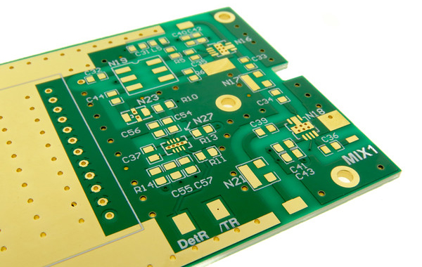
Case of Supporting PCB Manufacturing France Projects by EBest Circuit (Best Technology)
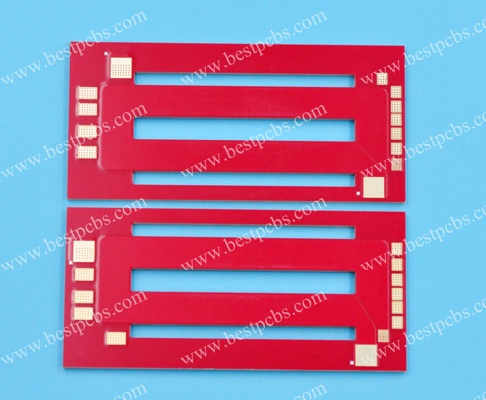
This 4-layer FR4 PCB was manufactured by EBest Circuit (Best Technology) for a leading French industrial automation company specializing in high-precision servo drives. The board serves as the main control unit in their latest generation of servo drivers, which are deployed in automated manufacturing lines across France’s automotive and aerospace sectors. The application demands exceptional reliability under continuous thermal stress and vibration, making the TG170 high-temperature material essential for stable performance in industrial environments where ambient temperatures can reach 45°C+.
Technical Specifications:
- Layer Count: 4 layers
- Base Material: FR4, TG170
- Material Type: S-10002M
- Copper Thickness: 1oz/0.5oz/0.5oz/1oz (outer/inner layer distribution)
- Board Thickness: 1.6mm +/-10%
- Surface Finish: ENIG (Immersion Gold with Au thickness 1μ”)
- Solder Mask: Black
- Silkscreen: White
- Special Requirements: Impedance control
The impedance-controlled PCB ensures signal integrity for high-speed communication between the processor and power modules, while the ENIG surface finish provides excellent planarity for precise component placement and reliable wire bonding. The black solder mask meets the client’s aesthetic requirements for their premium product line, with the high TG material ensuring dimensional stability during thermal cycling in demanding industrial environments. This project demonstrates our capability to meet the stringent requirements of French industrial customers with complex, reliability-driven applications.
To conclude, PCB Manufacturer France signifies a commitment to quality, reliability, and technical partnership for industries within the French market. This article has outlined the key aspects of selecting and working with a trusted PCB fabrication partner for projects in France. For French clients seeking a balance of world-class quality, advanced capabilities, and cost-effectiveness, EBest Circuit (Best Technology) stands as a reliable PCB manufacturer USA and European clients can depend on. Our expertise in complex and standard PCBs ensures your projects are in capable hands. Reach out to our team at sales@bestpcbs.com to get a quote for your next project.