PCB manufacturing PCB manufacturing
Home > Blog

Thermal Conductivity—Aluminum PCB vs Ceramic PCB Series 2

April 19th, 2022

Last time we have talked about the structure difference between the aluminum PCB and ceramic PCB. So, based on the different structures, whose thermal conductivity is better?

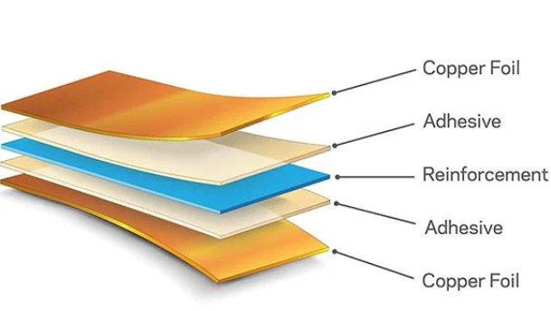
We have known that a single layer aluminum PCB is made up of copper layer, dielectric layer and aluminum layer. Meanwhile, the dielectric layer is the decisive factor affecting the thermal conductivity.

Generally, its thermal conductivity ranges from 0.8 to 3.0 W/m-K, but can up to 8.0 W/m-K. So, in terms of heat dissipation, the aluminum substrate does much better than FR-4 substrate. And it is a good choice for LED lighting products with high power.

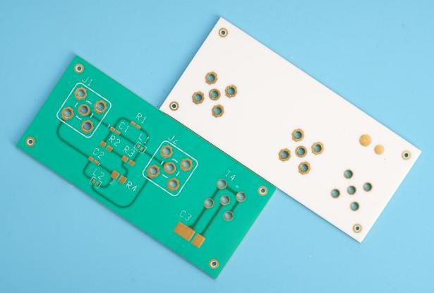
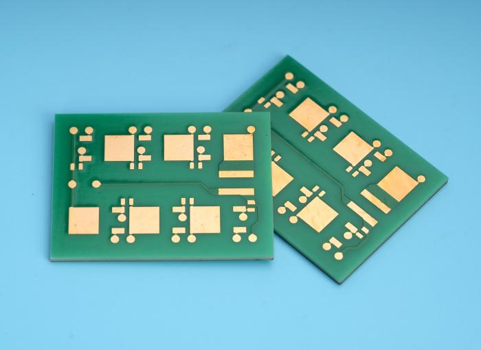
Aluminum PCB

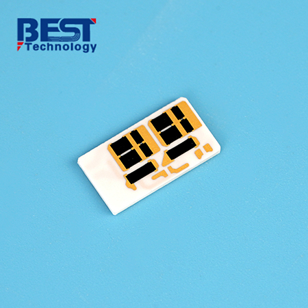
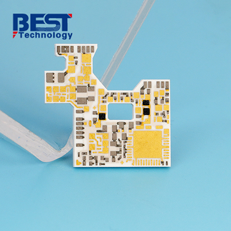
However, the heat-conducting property of ceramic PCB is superior to that of the aluminum PCB.

Since ceramic itself is an insulating material with a great heat-conducting property, it does not need a dielectric layer. Therefore, the heat can be dissipated directly through the ceramic.

Because of its excellent performance in heat dissipation, it is particularly suitable for the lighting product with ultra high power and those products which have a high demand of heat dissipation.

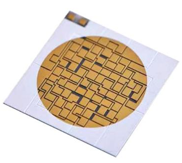
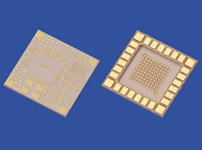
Ceramic PCB

To summarize, clearly, we can know from the table below that ceramic PCB does better than aluminum PCB in terms of thermal conductivity and heat dissipation. And this is mainly because of the dielectric layer, which is related to the functions of bonding, insulation and heat conduction.

The better the heat conduction performance of the insulating layer, the more conducive it is to the diffusion of heat generated during the operation to the device, hence it will be more conducive to lower the operating temperature of the device. That is to say, aluminum PCB will be subject to the dielectric layer, while ceramic PCB will not be restricted.    

And, this is the end of the comparison of the thermal conductivity between aluminum PCB and ceramic PCB. If you still have any questions about them, please feel free to contact us.

Electrostatic’ s Power-Trivia Series 2

April 18th, 2022

Last time we have known that electrostatic discharge (ESD) account for the highest proportion of causes leading to the failure of high electrostatic sensitive devices and the generation of it. Therefore, today we are going to talk about what kind of damage the static will cause to the Printed Circuit Board and how to avoid it.

The Influence of Electrostatic

Under different circumstances, the electrostatic voltage carried by the human body ranges from hundreds of volts to thousands of volts. And when people touch the electronic components, there will be ESD, resulting in the damage to devices and the reduction of reliability. To make matters worse, ESD will break down the device and directly scrap the product.

PCBA

Besides, the ESD will lead to a large pulse current, which will generate a lot of heat in the chip and printed circuit board, making them burn out. Moreover, the integrated circuits (IC) are built with denser lithography lines than before so that their ability to withstand electrostatic discharge becomes weaker. Therefore, it is necessary to prevent it.

Elimination of Electrostatic

Since the static will has a great impact on the PCB and electronic components, it is extremely significant to take precautions against the electrostatic by taking some measures. And here are some measures carried for eliminating the electrostatic in our workshop.

  • Putting on anti-static clothes and hats. It is to prevent static existing in clothes and hair from influencing the board.
Anti-static Clothes and Hats
  • Wearing anti-static wrist straps. The principle is to discharge the static from the human body to the ground through the wrist strap and grounding wire.
Anti-Static Wrist Strap
  • Using static elimination instrument. What we have to do is to put just one hand on static elimination instrument, and do not leave our hand from it until the red light turns to green, which aims to eliminate the static existing in our body.
Static Elimination Instrument
  • Keeping a certain humidity in the workshop. Higher humidity is not prone to ESD. The higher the humidity is, the easier it is to conduct electricity. As a result, electrostatic cannot be stored in our body.
  • Using anti-static packaging. When packaging, we have different packaging ways, such as anti-static bags, anti-static bubble film and so forth. And what to be used in packaging is up to our clients.
Anti-static Bags

To sum up, electrostatic will cause damage to the Printed Circuit Board and electronic components so that it is necessary to take some measures to prevent it.

And this is the end of this trivia. If you would like to know more about PCB, you are welcome to contact us.

Electrostatic’ s Power─Trivia Series 1

March 23rd, 2022

The Introduction to Electrostatic

Static, the excess charge on an object, is a phenomenon caused by the unbalanced distribution of charge in the material system. When an object is charged, the charge will remain on the object unless it is removed by other objects, so it is called “static electricityâ€.

As is known, we cannot touch PCB directly with our hands because of the electrostatic. But most of people have thought lowly of electrostatic’ s power, deeming that it is not strong enough to be harmful to some devices, especially electronic components.

On the contrary, electrostatic can be in some way devastating. According to the statistics, electrostatic discharge (ESD) account for the highest proportion in the ranking of causes leading to the failure of high electrostatic sensitive devices, which is 59%.

Pie Chart

The Generation of Electrostatic

There are various ways resulting in the generation of electrostatic. But, triboelectrification, namely indicating that electrostatic is generated by friction, is the most common one.

Where there is friction, there will be electrostatic. When walking, the shoes will rub with the floor, leading to the triboelectrification. Also, the frictions between our hair and clothes are so easier to generate the static that every movement in the PCB workshop will unintentionally cause the generation of static.

Then the static generated will have a great impact on the PCB and electronic components. But, how great the electrostatic’ s power is, or in other words, what kind of damage can it cause to the printed circuit boards or electronic components? And what can we do to eliminate the electrostatic?

We will talk about it next time, hence if you would like to know more, you are welcome to contact us, or you can continuously follow our blog site, on which we will keep sharing more information about PCB.

Differences in Structure——Aluminum PCB vs Ceramic PCB Series 1

March 21st, 2022

It is supposed that we are familiar with both aluminum PCB and ceramic PCB. But if juxtaposing them, which one will be better by one tally? So, we are about to talk about some differences between them in terms of structure.

Aluminum PCB

Aluminum substrate namely uses aluminum as substrate, which has a good heat dissipation capacity. Generally, it is single-sided, and also can be double-sided while multi-layer aluminum PCB is a little bit hard to manufacture. Besides, a single layer aluminum PCB is made up of copper layer, dielectric layer and aluminum layer.

Structure of Aluminum PCB

Ceramic PCB

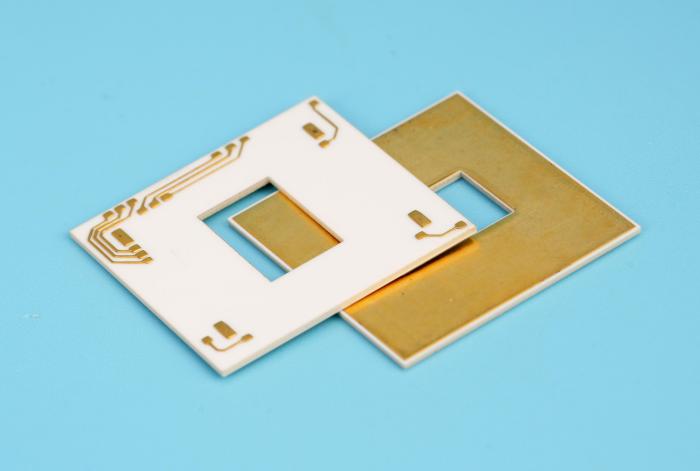
Ceramic PCB namely uses ceramic as substrate. Apart from the material, the structure is the biggest difference between ceramic PCB and aluminum PCB. Since ceramic itself is an insulating material, it does not need a dielectric layer. Its structure is as follows.

Structure of Ceramic PCB

Therefore, whether there is a dielectric layer is the main difference in structure between aluminum PCB and ceramic PCB. And dielectric layer plays an important role in thermal conductivity. So, what is the relationship between dielectric layer and thermal conductivity? And whose thermal conductivity is better between aluminum PCB and ceramic PCB?

We will talk about it next time. And if you would like to know the answer, please feel free to contact us, or you can continuously follow our blog site, we will keep updating more information about the differences between aluminum PCB and ceramic PCB on it.

What Should be Prepared Before Starting the SMT Process?

February 15th, 2022

SMT, whose full name is Surface Mounted Technology, is the most popular technology in electronic assembly industry. It refers to process on PCB (Printed Circuit Board), putting various electronic components on PCB, such as resistors, capacitors, inductors, and so forth. Also, there are some dos and don’ts in the whole process of PCBA.

As noted previously, there are all sorts of electronic components that will be used in the assembly process of Printed Circuit Board. Therefore, it is extremely important to take some measures to keep a check on static. Here are three steps before entering the SMT workshop.

First, put on anti-static clothes and hats. It is to prevent static existing in clothes and hair from influencing the board, for static has a potential and tremendous destructive power.

Anti-static Clothes and Hats

Second, what we have to do is to put just one hand on static elimination instrument, and do not leave our hand from it until the red light turns to green, which aims to eliminate the static existing in our body.

Static Elimination Instrument

Third, across the air shower door. In this way, dust that is invisible on our body can be blown off in about 5 seconds.

Air Shower Door

Only finishing the three steps above can we enter the PCB assembly workshop. And after entering the workshop, there are also something needed to be prepared.

  • Solder paste. The storage temperature of solder paste is 2-10 degrees Celcius, hence it has a period of regaining temperature, which conducts in the rewarming machine for 4 hours. Then the solder paste should be rabbled in a blender for 5 mins in order to help three ingredients in it to be fully integrated, which can help to achieve a better printing and back-flow soldering effect.
Solder Paste
  • Oven. This machine is used to get rid of the moisture from materials or boards, ensuring that PCB will not be defective due to moisture during the subsequent assembly process. Moreover, different boards have different requirements. But generally, the baking parameter is 105 degrees Celcius, lasting 1.5 hours.
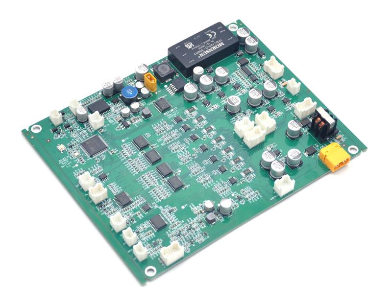
Oven
  • Dryer. It is used to maintain a set temperature and humility of materials and boards that needs to be processed that day, which is also to avoid that moisture does harm to materials and boards after removing the moisture by oven.
Dryer
  • Tension test of stencils. Before manufacturing, the stencils’ uniformity should be tested by tensiometer, which mainly tests the four corners and the center part of the stencil, guaranteeing the solder paste printing quality. And the parameter should be between 30 and 45.
Stencils

To sum up, although there are lots of preparations should be done before starting the formal assembly process, each of them is significant, for they will probably influence the quality of boards directly. Besides, only a good preparation can make a certain that the follow-up process can keep going. Thus, it is a must to prepare well in advance.

And EBest Circuit (Best Technology) is an experienced electronic company. It not only can provide PCBA service, but can provide other services, such as FPC, FR4 PCB, Rigid-flex PCB and so on. And if you have any questions about SMT, or any other questions about assembly, you are welcome to contact us.

Advantages of LED PCB Compared with Common Standard PCB

December 22nd, 2021

With the development of electronic products, the requirements of circuit boards applied in electronic products are becoming higher and higher. The volume of printed circuit boards is also shrinking exponentially, the assembly density is increasing, and the internal wiring of the line layer is becoming more and more intensive. Compared with PCB, LED PCB with metal core can achieve better heat dissipation effect.

LED PCB material:

First of all, LED PCB space utilization is higher, it takes up relatively small space, but can withstand relatively high-power output.

It is well known that when the power of the circuit board is high, high heat will be generated. If the heat cannot be dispersed in time, it may lead to the shortening of the working life of LED products, and the more serious consequence is the safety problem of the circuit board due to overheating.

Therefore, in order to make the LED lighting system longer life, it is generally used to print the circuit board with metal core, and the characteristics of the metal core is relatively large density, strong thermal conductivity, conducive to heat dissipation effect.

LED PCB board design:

The LED PCB is also unique in that its components are located on the surface, rather than through holes, because the metal core at the bottom dissipates heat more quickly.

LED PCB surface mounting

Some LED printed circuit boards have through-holes, especially multilayer metal core printed circuit PCB. Because the number of layers of the circuit board increases, the circuit layout is more complex, heat is more difficult to emit, and the existence of the through hole is to achieve faster heat dissipation. The drilling holes on the LED board are mounting holes, which are usually larger than the standard PCB through holes.

LED PCB solder mask color:

In addition, LED printed circuit board solder resistance layer color is also its characteristics.

The color of solder resistance layer on the LED printed circuit board is usually white, while the PCB board has a series of colors such as black, green and red and so on. This is also determined by the characteristics of LED boards in practical applications. Since LEDPCB board is usually used as backlight board, photosensitive solar ink is usually coated on the surface of the circuit board. White Taiyo Solder mask can achieve high temperature resistance, not easy to change color, high reflectivity, so as to achieve the reflection effect of lighting and better lighting effect.

LED PCB

Via Tented, Via Filled & Via Plugged

December 20th, 2021

Via Tented, Via Filled (filled with solder mask) & Via Plugged (Via In Pad – Conductive material or Non-Conductive material)

One of the most confused idea during our PCB design is the difference between Via Tenting, Via Filling and Via Plugging. Designers often get mixed up between them and fail to take full advantage of the process.

Today, let us discuss them, so that you can be confident in specifying your design requirements clearly when submitting PCB files to EBest Circuit (Best Technology) before final manufacturing.

Via Tented

What is via?

A plated through hole (PTH) in a Printed Circuit Board that is used to provide electrical connection between a trace on one layer of the Printed Circuit Board to a trace on another layer. Since it is not used to mount component leads, it is generally a small hole and pad diameter.

A. Three methods and definitions of via processing

There are three methods for via processing: via hole opening & via hole cover oil & via hole plug oil

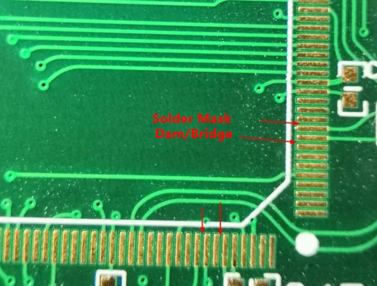
1. Through hole opening window: it is the tin on the solder ring of the via (the tin is exposed like a plug-in pad). The window is usually used to debug the measurement signal. The disadvantage is that it is easy to cause a short circuit.

2. Through hole cover oil: it is the welding ring of the through hole (via) covered with solder mask ink

3. Through hole plugging oil: refers to plugging the hole with ink.

Secondly, the inspection standards for a processing method

1. Through-hole opening window is like a plug-in pad, and the window is sprayed with tin. Inspection standard: tin can be tinned, and tin can be easily tinned.

2. The inspection standard of the via hole cover oil: it is not easy to tin in the patch.

3. Inspection criteria for via plug oil: First, it must be opaque, and it must be covered and blocked by ink.

Finally, we are talk for comparison and distinction between via hole cover oil and via hole plug oil:

1. Via plug oil This process is an important supplement to via plug oil, so generally high-quality boards will require via plug oil. And often many engineers who are just entering the industry are stupid and unclear. So how do you distinguish between the two?

2. The requirement of via hole cover oil is that the ring of the via hole must be covered with ink. The emphasis is to ensure the thickness and coverage of the ink on the edge of the hole. The key control is that the ring does not accept false copper exposure and orifice oil. Thin

3. Through hole plugging oil is the production of plug holes with ink inside the holes of the through holes. The emphasis is on the quality and density of the plug holes. After the holes are plugged, no light can be transmitted.

4. The method of plugging the via hole is to first fill the via hole with ink to block the via hole, so that the ink on the solder mask will not flow into the via hole, so as to achieve the situation that the via hole does not appear yellow. (If you have strict requirements and place an order for via hole cover oil, the cover oil is usually not full or yellowish, you can change it to via hole plug oil later). In addition, the smaller the vias are, the easier it is to plug them. The vias of the fortress oil are not easy to be too large (the circuit board proofing plugging oil is directly plugged with ink, and the printing tape is plugged. It is recommended that the vias that need to be plugged are designed to be <0.5mm. This is also free; no additional money is required).

If you have more question Via Tented, Via Filled& Via Plugged, warmly welcomed to contact Best Tech for more FR4 design service.

What is PI heating film?

December 20th, 2021

With people’s pursuit of high-quality life, now many electronics products are designed including heating film. It is kind of emerging material in the current industrial development.

The heating film is divided into different temperature resistance grades due to the different materials, and it can be divided into different names due to the different internal heating mechanisms.

Today let us mainly to introduce the Flex heating film, which conductor is made of Polyimide film (PI), people also called it PI heating film, Kapton Polyimide Heater, Kapton heating film or Polyimide Heating Plate.

Flexible PI Heating Film is designed with various resistance circuits according to the customer‘s request, which use Polyimide film (PI film) as the outer insulator, and use metal foil as the inner conductive heating element, to laminate both materials together by high temperature and high pressure.

You can know more details about the Flex heating film when you check below stack up and photos.

As Polyimide Heater is kind of surface heating material, which forms the maximum heat conduction surface with the heated body, so such heating method has very good conductivity, and with the characteristic of fast heating and low thermal inertia

It can withstand 300 ℃ high temperature in the short term, and work below 160 ℃ in the long term.

In other hand, the thickness of the flex heating film is between 0.13-0.3mm, which makes such product very flexible and light, and occupies very small space on the entire product design. So Flex heater is very good for using on the situations where space and weight are limited, or where the heater is exposed to vacuum, radiation, oil or certain chemical substances.

Here the list for where the Flex heater mainly used in:

1. Heating of household appliances

2. Under cold environmental conditions, make the instrument reach the designed working temperature, such as camera defogging heating.

3. Vacuum heating and baking field

4. Car rearview mirror defrosting, radar snow removal, defrosting, etc.

5. Medical care and beauty equipment industry

The following are some products which includes the flexible Polyimide Heater inside.

Believe it will supply a good reference for you to know this product.

So, as you can see that the product with Flex heating improve highly for our life quality.  Our company has more than 15 years experiencing on manufacturing Flex PCB and Flexible heating film, if you are interesting to know more manufacturing details about PI heating film, you are welcome to contact us.

What is LED Thermal Management?

December 20th, 2021

LED lighting (Light Emitting Diodes) can provide more lumens per watt than incandescent bulbs, and the amount of light emitted does not depend on the size or shape of the bulb. It has significantly smaller footprint, higher efficiencies and lasts a long time.

One of the big challenges of LED lighting is LED Thermal Management, since around 70% of the electricity used by an LED becomes heat, and LEDs work best around room temperature, if the heat is not managed with some sort of thermal management solution, it can result in reduced efficiency in the LED, shorten the life of the bulb itself, and possibly causing damage to other components near it. In this context one of the best places to start with would be thermal management within the Metal Core PCB.

Thermal Management in MCPCB

If you are using LED power, there are chances that you would encounter problem at or above 80 watts. For example if you are considering application like the street lighting which might require up to 150 watts per lamp, led thermal resistance at such high power point would be a cardinal concern.

MCPCB can be created using a wide range of heat-dissipating materials without changing the LED component. From copper which offers better thermal conductivity to aluminum which is cheaper to specialized MCPCB using coated steel, ceramics or many other options. To address the LED thermal resistance issues and achieve optimum thermal management using LED, external heat sinks can also be used. This facilitates dissipation of exceptionally large amount of heat.

In fact on an average MCPCBs have several different shapes and degrees of heat dissipation profile. However the most challenging ones are no doubt the types in which the LED applications have to be stored in airtight enclosure to protect from the environment around. Thermal management in this case could be anything from air-to-air heat exchangers to using internal fans to even heat transfer via a series of conduction and convection alternatives.

Thermal Management of MCPCB

Thermal management is important for the electronic systems to encompass the processes along with the technologies.The main objective of thermal management is to ensure the temperature remains consistent for the functional and absolute maximum limits. The temperature exceeding the limit may cause destruction physically or may lead to a system failure. Therefore, MCPCB is essential because efficient thermal management increases the feasibility, enhances durability, and reduces the failure rates.

It also enables the high circuit density design for the users. Basically, thermal conductivity is a specific material from a property with the ability to conduct proper heat management as soon as it enters into the system. The conventional PCB share less thermal conductivity and also not capable enough to meet the increased demand for the thermal constraint required for high power dissipation PCB. The best alternative to solve this problem is the Metal Core Printed Circuit Board.

If you have any questions about MCPCB, welcome to contact EBest Circuit (Best Technology).

Does ceramic PCB is suitable for SMT

December 20th, 2021

Ceramic PCB is becoming more and more popular due to ceramic PCB with a lot of advantageous performance.

  1. For example, ceramic PCB with good anti-abrasive function because with palladium, the more palladium, anti-abrasive function is better.
  • Ceramic PCB is very good for withstanding high and low temperature too, -55 degree to 850 degrees.
  • Ceramic PCB with great heat dissipation function, ceramic PCB can conduct the heat away very fast and keep the working temperature stable.
  • Ceramic PCB with great heat dissipation function, the thermal conductivity is much better than other PCB, it is very good for high power LED lighting application.

All the ceramic PCB is suitable for SMT, but the SMT is a different from other PCBs, need to control the temperature strictly, and also need to pay high attention to hand it, because ceramic PCB is very fragile, it can be broken very easily.

Please contact sales@bestpcbs.com to know more about ceramic PCB with SMT.