SMT contract manufacturing is an essential solution for businesses that aim to combine high-quality electronics production with operational efficiency. This blog provides a comprehensive overview of SMT contract manufacturing, highlighting its processes, industry applications, advantages, challenges, and how EBest Circuit (Best Technology) delivers reliable, high-quality, and customer-focused SMT solutions.
Do you face any of the following challenges in SMT contract manufacturing?
- Design-to-Manufacturability Mismatch: Many clients find that PCB layouts or component placements are not fully compatible with manufacturing processes or assembly equipment, causing line adjustments or repeated rework.
- Unstable Component Supply and Lead Times: Delays or shortages of critical components disrupt production schedules and extend time-to-market.
- Inconsistent Soldering Quality: Issues in solder paste printing, component placement, or reflow soldering—such as insufficient solder joints, bridging, or tombstoning—can reduce yield and reliability.
- High-Density / Multi-Layer PCB Assembly Challenges: Complex BGAs or multi-layer PCBs are prone to misalignment or thermal stress during precise placement and soldering.
- Balancing Cost and Delivery: Customers often struggle to achieve fast delivery without compromising quality, especially for prototypes or small-batch, customized orders.
Here are the proven solutions EBest Circuit (Best Technology) applies to address these challenges:
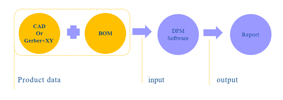
- Professional Design Review and DFM Support: Our engineering team conducts in-depth DFM (Design for Manufacturability) analysis before production, optimizing PCB layouts and component selection to ensure designs are fully compatible with manufacturing processes, minimizing rework and risk.
- Reliable Supply Chain Management: We maintain long-term partnerships with top-tier distributors like TI, Mouser, and Digi-Key, with strict incoming inspection to guarantee on-time delivery of 100% genuine components.
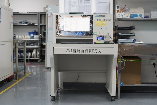
- Advanced Process and Quality Control: Full-process quality monitoring with SPI (Solder Paste Inspection), AOI (Automated Optical Inspection), and X-Ray inspection ensures consistent soldering quality and maximizes yield.
- High-Precision Multi-Layer PCB Assembly: Our high-speed pick-and-place machines, reflow ovens, and selective soldering systems support complex BGAs and dense multi-layer boards, ensuring precise placement and reliable solder joints.
- Flexible Production and Cost Optimization: Using MES-managed scheduling, we provide rapid prototyping, small-batch trial runs, and large-scale production while maintaining the optimal balance between cost and delivery time.
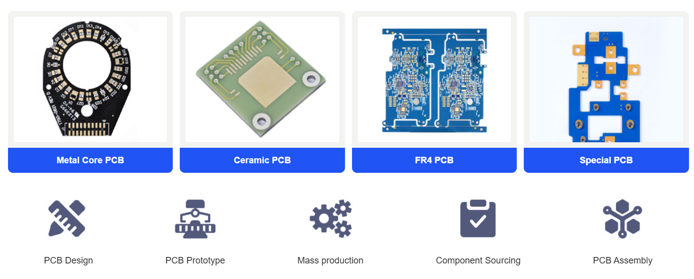
EBest Circuit (Best Technology) is a professional turnkey EMS PCB manufacturer. We have provided PCB contract manufacturing and SMT contract manufacturing services in a very competitive market for 20 years. We have our SMT factories in China and Vietnam, where we can schedule your PCBA order with a quite quick delivery time. If you have any specific needs about PCB or SMT solutions, just feel free to reach out to us at sales@bestpcbs.com.
What is SMT Contract Manufacturing?
Surface Mount Technology (SMT), short for Surface Mount Technology, is the prevailing assembly method in the modern electronics industry. SMT involves placing pinless or short-lead components, also called Surface Mount Devices (SMDs), directly onto the surface of Printed Circuit Boards (PCBs) or other substrates. These components are then soldered using precise reflow or wave soldering processes, creating a highly reliable electrical assembly.
In the context of manufacturing, SMT contract manufacturing refers to outsourcing this assembly process to specialized providers, also known as Electronics Manufacturing Services (EMS) providers. These contractors take responsibility for component placement, soldering, inspection, and quality assurance, allowing client companies to focus on design, innovation, and market deployment.
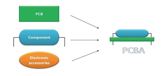
Key distinctions: It is important to clarify the difference between PCB and PCBA. A PCB (Printed Circuit Board) is simply the bare board with conductive tracks, while a PCBA (Printed Circuit Board Assembly) is the completed board with all components soldered in place. SMT is the core technology used in the assembly process, turning a PCB into a fully functional PCBA.
Forms of Contract Manufacturing: Contract manufacturing in electronics generally exists in three forms:
- Full Turnkey Services: The manufacturer handles procurement of components, assembly, testing, and delivery.
- Consignment or Partial Services: The client provides components, and the contractor focuses on assembly and quality control.
- EMS Hybrid Models: Combining aspects of both full turnkey and consignment approaches, tailored to the client’s specific needs.
Contract manufacturing is sometimes also referred to as outsourced assembly, EMS services, or simply electronics manufacturing services. In all cases, the contractor assumes responsibility for the manufacturing process, allowing the client to reduce operational complexity and improve scalability.
SMT in Manufacturing: In manufacturing terminology, SMT specifically refers to the assembly technology, whereas “SMT contract manufacturing” describes the business model of outsourcing this technology to professional providers. This approach ensures precise component placement, consistent quality, and scalability—critical factors for high-mix, low- to high-volume electronics production.
By leveraging SMT contract manufacturing, companies benefit from advanced assembly techniques without investing heavily in equipment or labor. Additionally, professional SMT contractors implement stringent quality systems, including ISO certification, automated optical inspection (AOI), and process monitoring, which mitigate risks associated with defects and production delays.
What are the Features of SMT Contract Manufacturing Companies?
Professional SMT contract manufacturing companies provide a combination of technical expertise, robust infrastructure, and quality assurance systems. Their key features include:
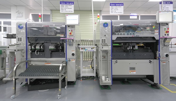
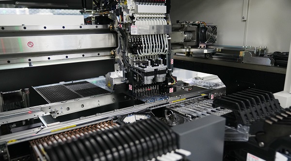
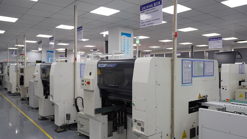
- State-of-the-art assembly equipment: High-speed pick-and-place machines, advanced reflow ovens, and selective soldering systems ensure precision and repeatability.
- Certified quality management: ISO 9001, IATF 16949, and other industry certifications demonstrate adherence to stringent standards.
- Engineering support: Experts provide DFM (Design for Manufacturability) reviews, optimizing PCB designs for production efficiency and yield improvement.
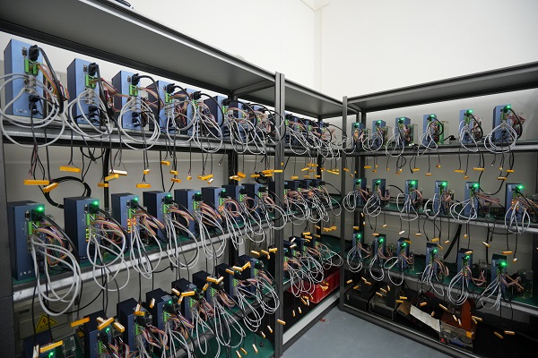
- Process transparency: MES systems allow real-time monitoring, full traceability of components, and immediate response to any assembly issues.
- Flexible production capacity: Facilities can handle both small prototype runs and high-volume production without compromising quality.
What is the Difference between SMT and SMC?
Understanding the distinction between SMT and SMC is critical for selecting appropriate manufacturing strategies.
SMT (Surface Mount Technology) is the assembly process used to mount components directly onto PCB surfaces, while SMC (Surface Mount Components) refers to the actual electronic components designed for SMT assembly.
Misunderstanding this difference can lead to procurement or assembly inefficiencies. Professional SMT manufacturers, like EBest Circuit (Best Technology), ensure that the process and components align perfectly for optimal performance and reliability.
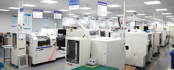
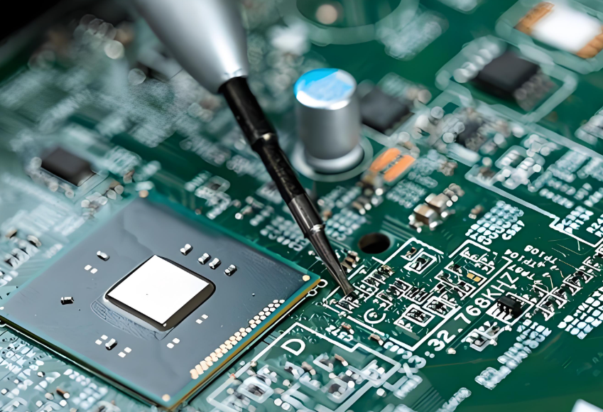
What is SMT Manufacturing Process?
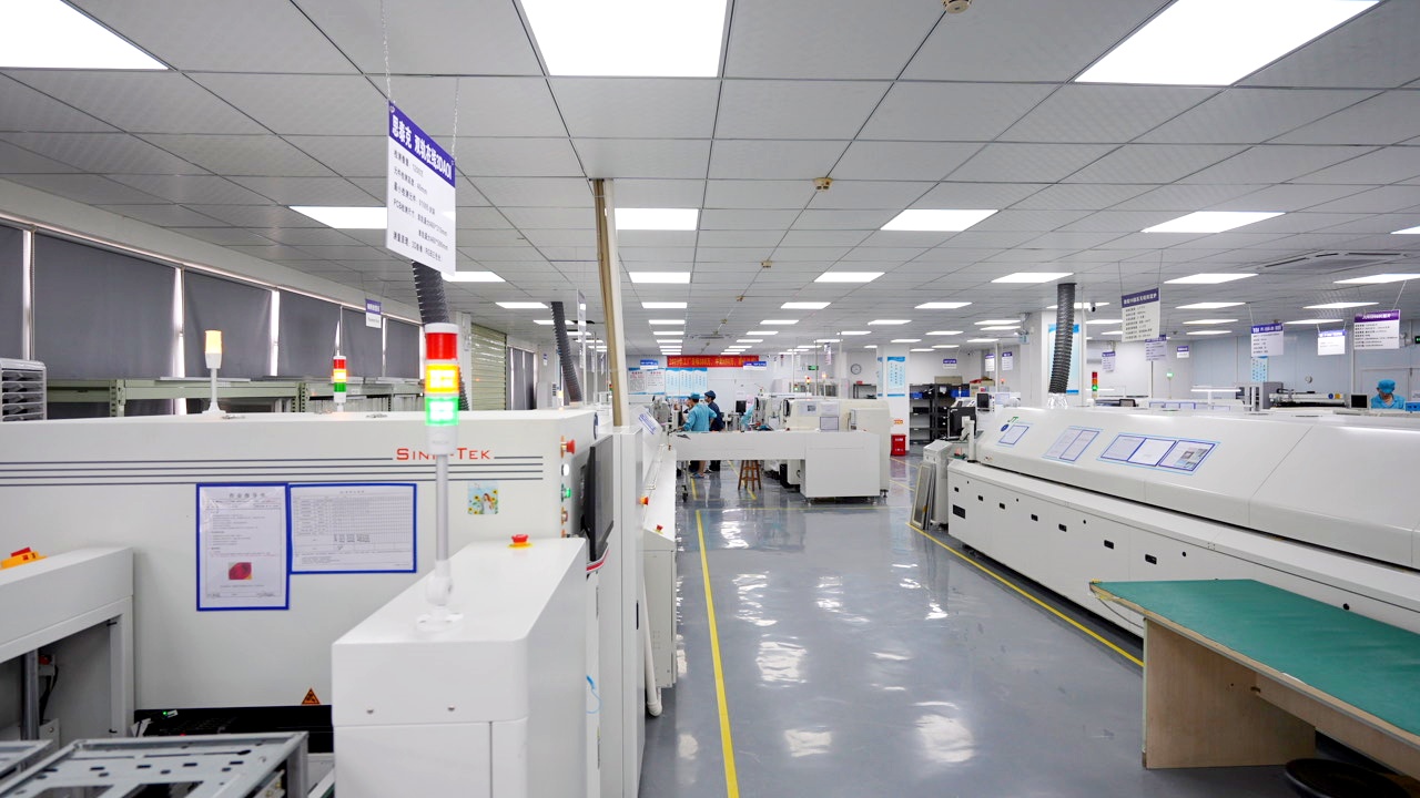
At EBest Circuit (Best Technology), the SMT manufacturing process is designed with precision and quality control at every step, ensuring high yield, reliability, and consistent performance for every PCB assembly. The process is structured as follows:
- Incoming Material Inspection (BGA/PCB)
All incoming components, including BGAs, and PCBs are carefully checked for damage, correct specifications, and storage conditions. This step prevents potential defects from entering the production line. - Pre-Bake
Moisture-sensitive components and PCBs are baked to remove absorbed moisture. This is essential to prevent soldering defects such as tombstoning or BGA popcorning during reflow. - Solder Paste Application
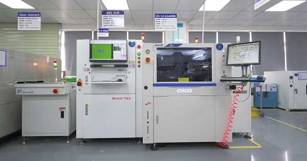
A stencil printer deposits solder paste precisely onto PCB pads. Accuracy here is critical: the correct solder volume and placement directly affect joint quality and reduce rework. - Solder Paste Inspection (SPI)
SPI is a key quality checkpoint. Using advanced 3D inspection systems, we verify the solder paste volume, height, and alignment on each pad. Any deviations are flagged immediately, ensuring that only boards with perfect solder paste deposits proceed to placement. This step significantly reduces defects in later stages and improves overall yield. - Component Placement
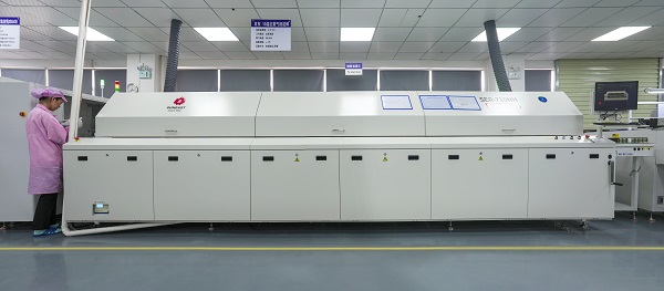
Automated pick-and-place machines position SMD components with high accuracy, even on complex multi-layer boards. Our machines are calibrated daily to maintain micron-level placement precision. - Reflow Soldering
PCBs pass through a precisely controlled reflow oven. The thermal profile is optimized to melt the solder paste while minimizing thermal stress on components, ensuring strong, reliable solder joints. - Post-Reflow Cleaning
Excess flux residues are removed to prevent corrosion and improve the longevity of assemblies. - Post-Oven Inspection
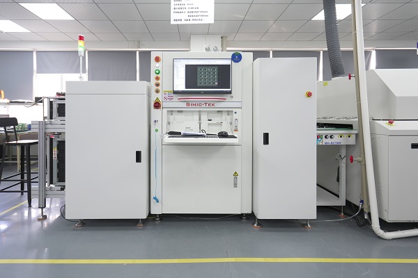
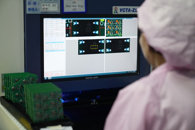
Visual inspection and automated optical inspection (AOI) ensure that no visible defects exist after soldering. - Automated Optical Inspection (AOI)
High-resolution AOI systems detect misaligned components, solder bridges, and other defects. This step acts as a final automated checkpoint before any manual corrections. - X-Ray Inspection (for BGA only)
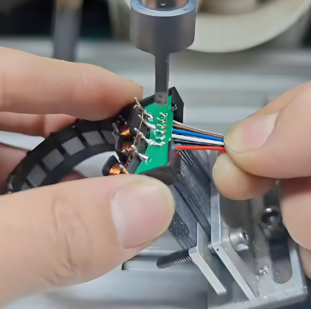
For BGAs and other hidden-pad components, X-ray inspection verifies solder joint integrity under the component. Boards without BGAs skip this step. - Secondary Soldering
Any through-hole components or rework areas are soldered using selective wave soldering or manual soldering. - Cleaning
Boards are thoroughly cleaned to remove any flux residues or contaminants, improving electrical performance and long-term reliability. - Programming / Functional Testing
Microcontrollers and programmable devices are programmed, followed by functional testing to ensure every PCB meets its electrical and functional specifications. - Conformal Coating and Potting
For enhanced protection, conformal coating or potting is applied, ensuring resistance against moisture, dust, and environmental stress. - Final Assembly
Boards are assembled into final products if required, with connectors, housings, or other components added. - Labeling, Routing, and Separation
All boards are labeled with traceable information, routed, and separated according to customer specifications. - Packaging and Shipment
Finished products are packaged using static-shielding bags, cut tape, bubble wrap, or blister trays as needed, ensuring safe transport to customers.
Professional Highlights:
- SPI inspection ensures every solder pad has correct volume and alignment before components are placed, drastically reducing defects.
- X-Ray inspection for BGA guarantees hidden solder joints are reliable—crucial for high-density boards.
- Functional testing combined with conformal coating ensures both performance and long-term reliability.
- Automated AOI and precision pick-and-place provide consistent results even for complex multi-layer boards.
By combining these detailed steps, our factory delivers SMT contract manufacturing that is precise, reliable, and highly professional, giving clients confidence that every PCB assembly meets rigorous quality standards.
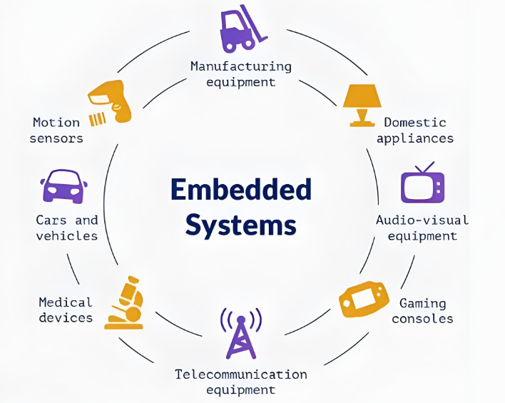
What Industries Use SMT?
SMT plays a pivotal role across multiple industries:
- Consumer Electronics: Smartphones, laptops, and wearable devices demand compact, high-performance PCBs.
- Automotive: Advanced driver-assistance systems (ADAS), infotainment, and power electronics require robust, high-reliability PCBs.
- Medical Devices: Precision and reliability are critical in diagnostic and therapeutic devices.
- Telecommunications: Networking equipment and high-speed communication devices rely on dense and precise PCB assemblies.
- Industrial Automation: Robotics, sensors, and control systems demand repeatable performance and high durability.
To put it simply, the versatility and precision of SMT make it indispensable in modern electronics manufacturing. By adopting SMT, companies across these industries can achieve high-density, reliable, and efficient PCB assemblies that meet strict performance requirements. Partnering with a professional SMT contract manufacturer ensures not only technical excellence but also consistent quality, faster time-to-market, and reduced operational risks. For industries where reliability, miniaturization, and precision are critical, SMT is not just a manufacturing choice—it is a strategic advantage.
What are the Pros and Cons of SMT Contract Manufacturing?
SMT contract manufacturing has become a cornerstone for companies seeking high-quality, efficient electronics production. By outsourcing surface mount technology assembly to experienced manufacturers, businesses can leverage advanced equipment, specialized engineering support, and rigorous quality control. Understanding the advantages and potential challenges of this approach helps companies make informed decisions and maximize the value of SMT contract manufacturing.
Advantages:
- High precision with reduced human error and consistent assembly quality.
- Lower operational costs compared to in-house assembly lines.
- Shorter production lead times for both prototypes and mass production.
- Access to specialized expertise in complex, multi-layer PCB designs.
- Improved scalability, allowing businesses to adjust production volume based on market demand.
Challenges:
- Dependence on the supplier for delivery schedules and production consistency.
- Effective communication and design alignment are crucial to avoid rework.
Given these factors, while SMT contract manufacturing presents some challenges, the advantages far outweigh them for companies aiming for high-quality, scalable, and cost-effective PCB assembly. By partnering with a professional and reliable SMT contract manufacturer, businesses can focus on innovation and market strategy, confident that their products will meet strict quality and performance standards. This approach not only reduces operational burden but also enhances competitiveness in today’s fast-paced electronics market.
Where to Get Contract SMT Manufacturing
When choosing contract SMT manufacturing services, companies are primarily concerned with risk and reliability. The ideal partner does more than just assemble PCBs—they ensure the success of your project while minimizing potential risks. EBest Circuit (Best Technology) is such a partner, offering professional, trustworthy SMT contract manufacturing solutions.
Our strengths can be summarized in five key areas:
- Turnkey Solutions with DFM Analysis
- Comprehensive services covering PCB fabrication, component sourcing and BOM management, SMT placement, THT insertion, testing, assembly, and final packaging.
- Our engineering team provides free in-depth DFM (Design for Manufacturability) analysis, proactively optimizing your design files to prevent potential manufacturing issues and cost waste, ensuring manufacturability and high yield.
- Comprehensive Quality Assurance and Traceability
- Our facilities are certified under ISO 9001 and IATF 16949, ensuring adherence to international quality standards.
- Production lines are equipped with SPI (Solder Paste Inspection), AOI (Automated Optical Inspection), and X-Ray systems for full-process monitoring.
- We maintain a complete material traceability system, allowing any product to be traced to its batch, machine, and operator, ensuring precise control of any issues.
- Transparent Supply Chain and Component Control
- Long-term partnerships with top distributors such as TI, Mouser, and Digi-Key guarantee 100% genuine components.
- Strict incoming inspection ensures all components meet standards before assembly.
- Extensive Industry Experience and Flexible Production Modes
- Deep expertise in automotive electronics, medical devices, industrial control, and communication equipment, understanding the strict reliability and certification requirements of each industry.
- Production lines are flexible, supporting rapid prototyping (1–2 days) to large-scale mass production, with efficient response to engineering changes.
- Professional Project Management and Seamless Communication
- Dedicated project managers and technical support teams for every client.
- Real-time system visibility of project status, material tracking, and production data.
In summary, EBest Circuit (Best Technology) provides a professional, reliable, and customer-focused SMT contract manufacturing service through full-process control, rigorous quality management, transparent supply chains, extensive industry expertise, and professional project management. Partnering with EBest Circuit (Best Technology) means lower project risk, higher product quality, and a smooth, efficient collaboration experience.
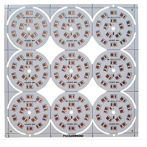
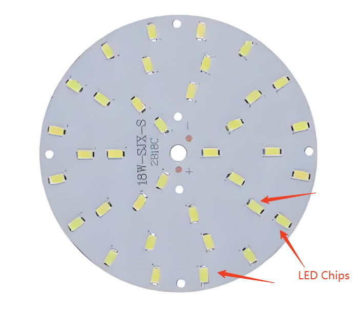
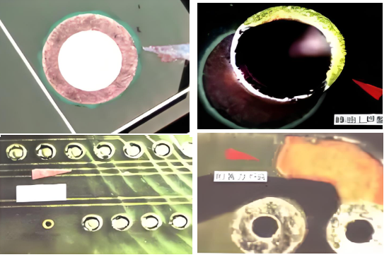
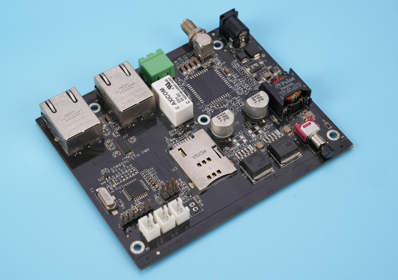
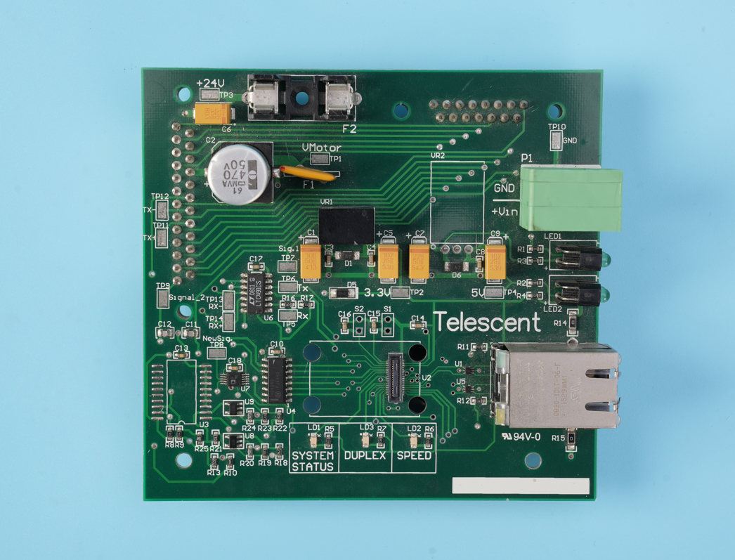
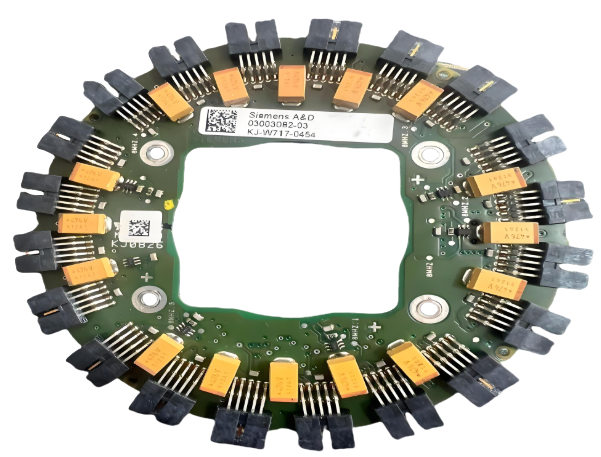
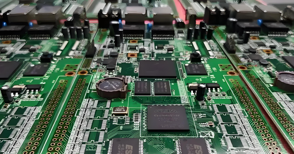
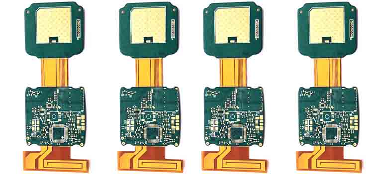
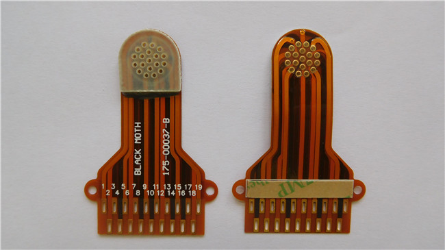
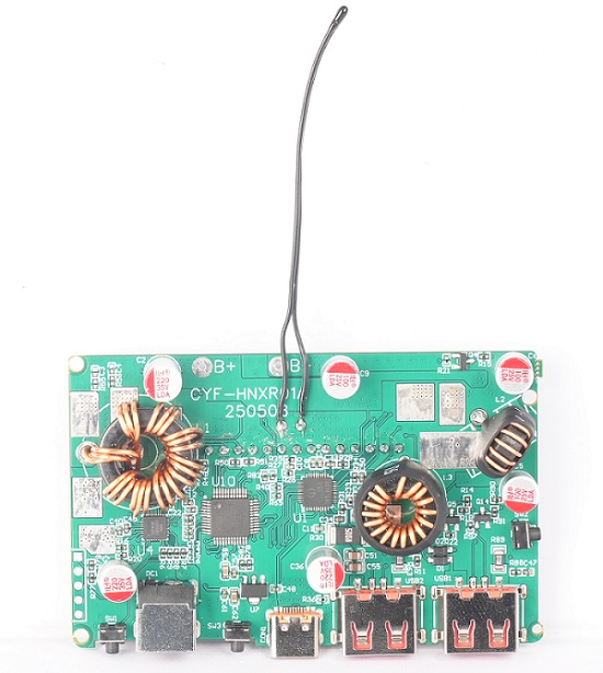
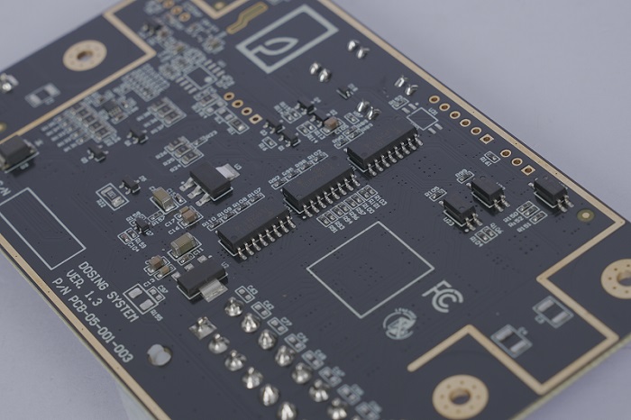
Case of SMT Contract Manufacturing in EBest Circuit (Best Technology)
At EBest Circuit (Best Technology), our contract SMT manufacturing services span multiple industries, including automotive electronics, medical devices, industrial control systems, and communication equipment. Our extensive industry expertise allows us to handle complex PCB assemblies that demand high reliability, precise tolerances, and strict adherence to industry standards.
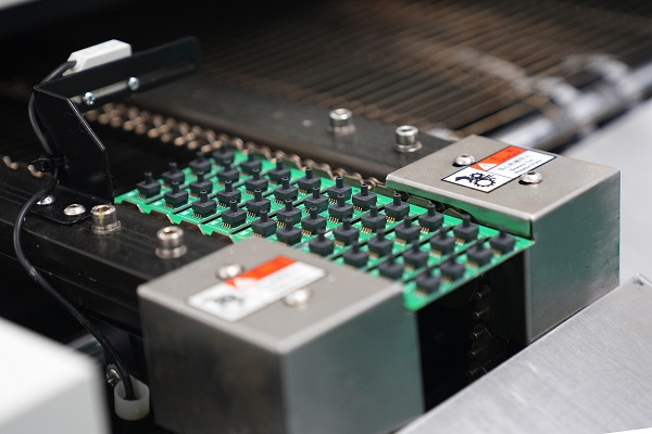
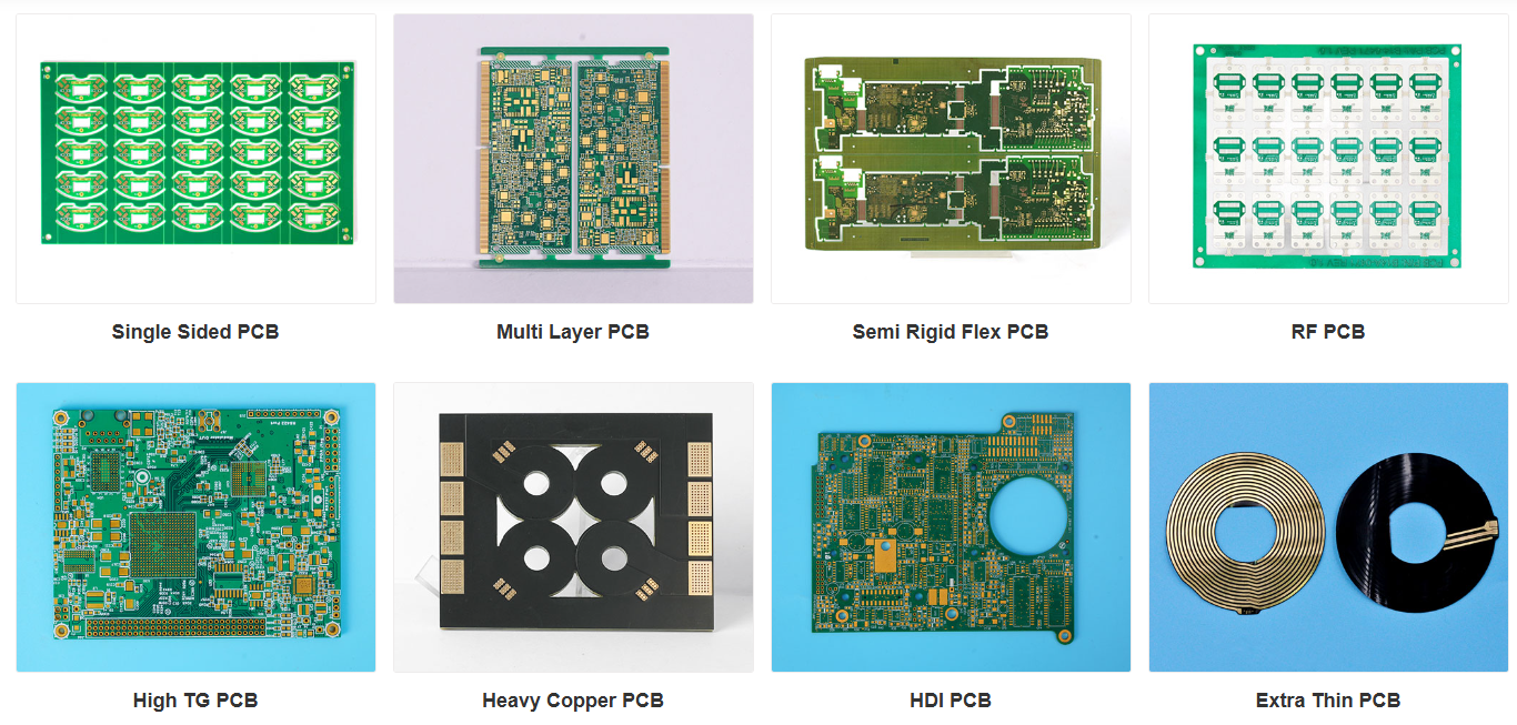
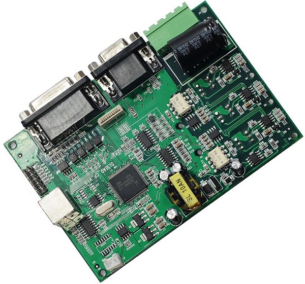
Here are some examples of actual PCBA boards we have manufactured for our clients:
- Automotive Electronics: Multi-layer PCBs for advanced driver-assistance systems (ADAS), in-vehicle infotainment, and power electronics. These boards require strict quality control, high thermal stability, and precise component placement.
- Medical Devices: High-density PCBs used in diagnostic equipment, wearable health monitors, and therapeutic devices. Reliability and traceability are critical in these applications.
- Industrial Control & Robotics: PCBA boards for industrial automation, robotics, and sensor control systems, requiring robust design and consistent performance in demanding environments.
- Communication Equipment: High-speed networking boards and RF communication devices where signal integrity and component density are key factors.
For each project, we implement automated AOI inspection, MES tracking systems, and dedicated engineering support, ensuring that every board meets design specifications and quality standards. We handle flexible production runs, from rapid prototypes to large-scale manufacturing, with rigorous testing at every stage.
This combination of industry expertise, technical capability, and end-to-end process control enables us to address customer pain points while providing reliability, repeatability, and transparency throughout the manufacturing process.
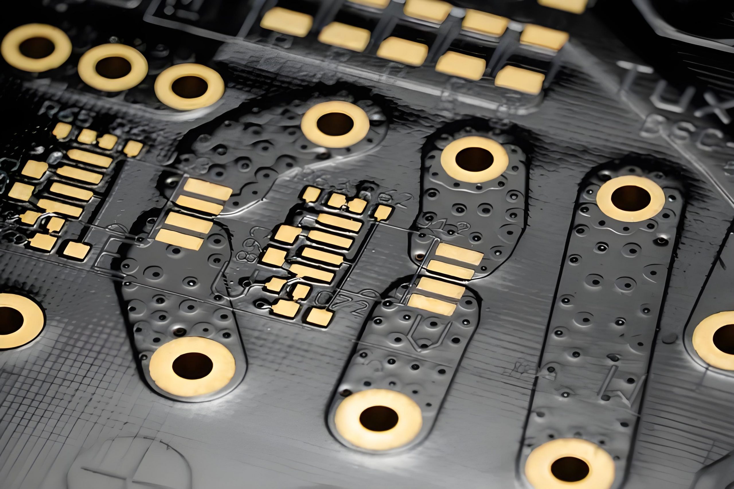
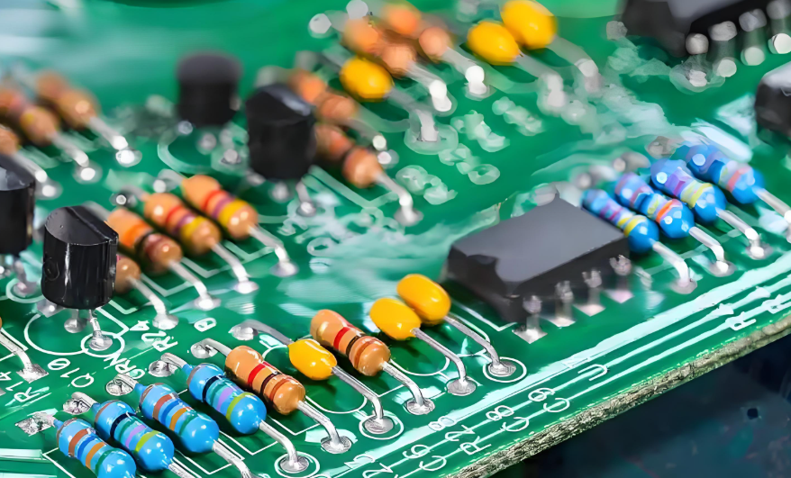
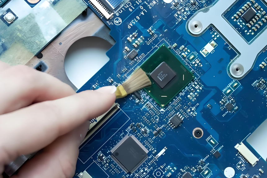
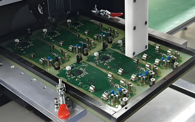
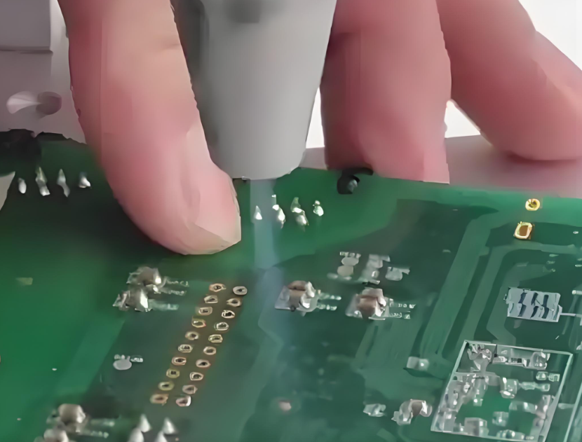
The images below illustrate the diversity and complexity of the PCBA boards we produce, showcasing the real-world applications of our SMT contract manufacturing services.
It is clear that, SMT contract manufacturing empowers businesses to achieve high-quality PCB production while focusing on their core competencies. For inquiries related to PCB design, prototyping, fabrication, or SMT contract assembly, please do not hesitate to contact us at sales@bestpcbs.com. Our team is here to provide expert support. As a turnkey EMS PCB manufacturer, EBest Circuit (Best Technology) provides superb quality China PCB manufacturing and EMS PCBA with Speedy Delivery services in a truly competitive market for nearly 20 years.