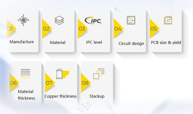
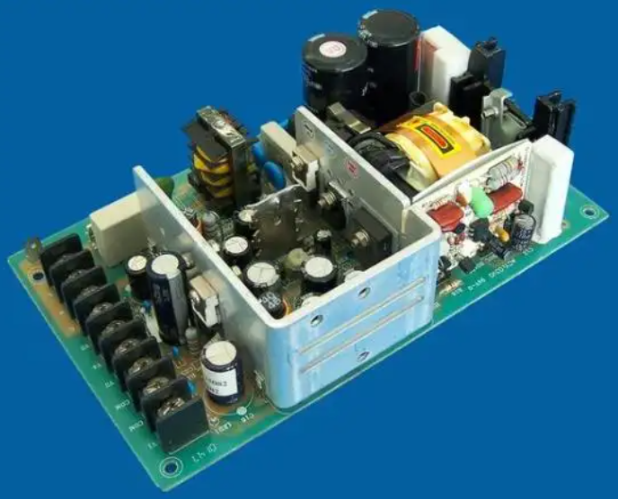
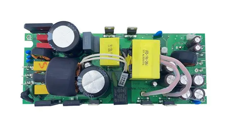
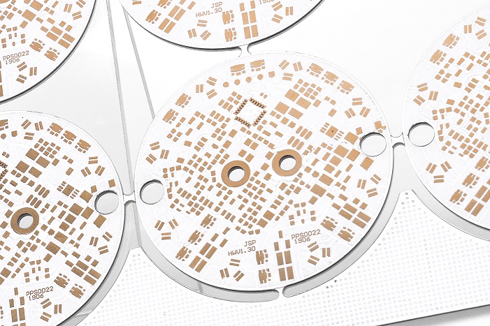
What is a 2 Layer Aluminum PCB?
A 2-layer aluminum PCB is a type of metal core circuit board that contains two conductive layers, usually copper, with an aluminum core or base material. Aluminum PCBs are used for their excellent heat dissipation properties, and always used in high-power applications like LED lighting, power supplies, and automotive systems. The aluminum base offers better thermal management than standard FR4 PCBs. In a 2-layer aluminum PCB, the two conductive copper layers allow more complex routing for electrical signals compared to single-layer boards.
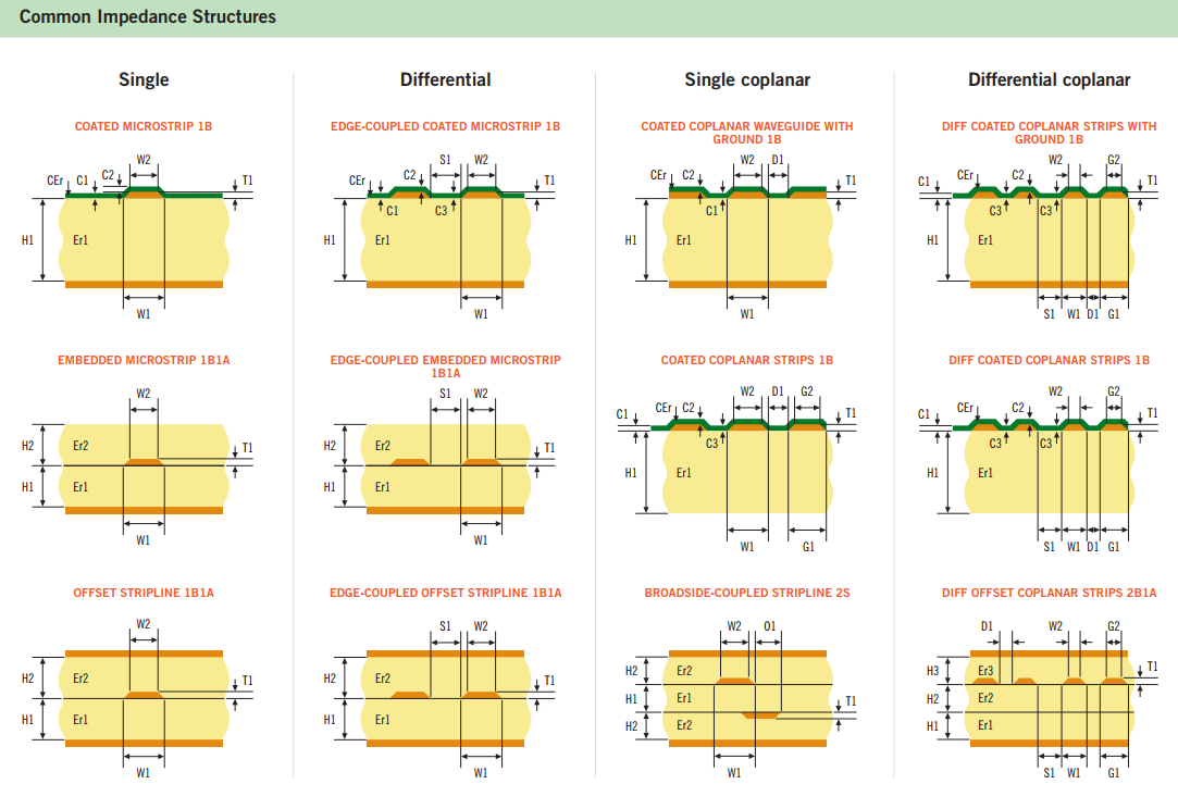
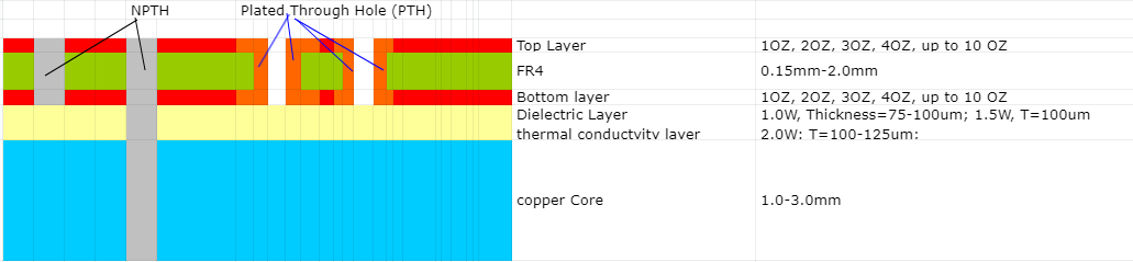
2 Layer Aluminum PCB Stack-Up
The stack-up of a 2-layer aluminum PCB consists of the following:
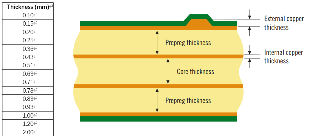
- Top Copper Layer: This is where the signal traces and components are located. It can vary in thickness, depending on current-carrying requirements.
- Dielectric Layer: A layer of insulation that separates the top copper layer from the aluminum core. It plays a key role in electrical isolation and heat transfer.
- Aluminum Base: This core provides structural support and excellent heat dissipation properties. It also serves as the grounding plane in some designs.
- Bottom Copper Layer: The second conductive layer allows for more advanced routing.
How Thick is a 2 Layer PCB Layer?
The thickness of a 2-layer aluminum PCB can vary depending on the specific design requirements, but typically, the copper layer is about 1 to 2 ounces (35 to 70 microns) thick. The aluminum base itself is thicker, usually between 1.0 mm and 3.0 mm, depending on the board’s required rigidity and heat dissipation needs. The overall board thickness generally ranges between 1.2 mm and 3.2 mm.
A thicker aluminum core improves heat transfer, but the board’s thickness must also align with the product’s mechanical and electrical requirements. Designers often have to balance between sufficient thermal performance and the overall board size for practical applications.
Is Thicker Aluminum PCB have Better Heat Dissipation?
Generally speaking, the thinner the thickness of the aluminum PCB, the faster the heat conduction speed. The thicker the thickness of the aluminum PCB, the slower the heat conduction rate. The thermal conductivity of aluminum-based circuit board mainly depends on its material and structure. Although thickness affects the path length of heat conduction, the more critical factors are the thermal conductivity and structural design of the material. For example, high thermal conductivity materials such as copper, silver and other high thermal conductivity materials will significantly improve the thermal conductivity of aluminum substrate. In addition, the thickness and thermal conductivity of the insulation layer will also affect the overall thermal conductivity effect .
Specifically, the thermal conductivity of the aluminum-based circuit board is also related to the thickness of its insulation layer. The thicker the insulation layer, although it can withstand higher voltage, it will also reduce the heat transfer efficiency. Therefore, choosing the appropriate insulation layer thickness and materials with high thermal conductivity is the key to ensuring efficient thermal conductivity of aluminum-based circuit boards .
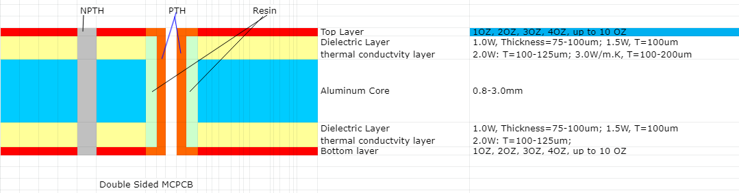
2 Layers Aluminum PCB vs. Double Sided Aluminum PCB
Though the terms “2 layers aluminum PCB” and “double-sided aluminum PCB” might sound similar, there are slight differences.
A 2-layer aluminum PCB contains two conductive copper layers. These layers can be arranged to handle signal routing and ground planes separately. In contrast, a double-sided aluminum PCB typically has one copper layer on either side of the aluminum core, offering less flexibility in routing. Here is the stack up of double sided aluminum PCB:
How Much Does Aluminum PCB Cost?
The cost of an aluminum PCB, including a 2-layer version, depends on several factors such as the board’s thickness, copper weight, design complexity, and production volume. On average, 2-layer aluminum PCBs cost more than single-sided aluminum PCBs because of the additional copper layer and routing complexity.
For small orders, prices might range between $5 and $15 per square foot. For larger production runs, costs can decrease significantly due to economies of scale. Factors like the thickness of the aluminum base and copper layer, as well as additional features like surface finishes, can also influence the price.
While aluminum PCBs are more expensive than standard FR4 boards, their enhanced thermal performance can reduce overall system costs by improving reliability and reducing the need for additional cooling measures.
How Many Layers Should a PCB Have?
The number of layers a PCB should have depends on the complexity of the design. For simple applications like LED lighting or power conversion, a 2-layer aluminum PCB is often sufficient. It provides more routing flexibility than a single-layer board while still offering effective heat dissipation.
For more complex designs requiring high-density interconnections or additional functionality, a multi-layer PCB with three or more layers might be necessary. However, multi-layer aluminum PCBs are rare because their primary function is thermal management, which is typically solved within one or two layers. The decision to use more layers depends on the specific application, power requirements, and signal integrity needed in the design.
Aluminum PCB Design Guidelines
When designing a 2-layer aluminum PCB, several factors must be considered to maximize performance:
- Thermal Management: Since aluminum PCBs are chosen for their thermal properties, optimizing heat dissipation is critical. Components that generate significant heat should be placed near the aluminum core, allowing for faster heat transfer.
- Copper Thickness: The copper thickness should match the current-carrying requirements of the design. Using thicker copper can help manage higher current loads, but it also increases the cost and weight of the PCB.
- Dielectric Layer: The thickness and material of the dielectric layer play a crucial role in both thermal and electrical performance. A thinner dielectric layer improves heat dissipation but may limit electrical isolation. Choosing the right dielectric material is key for balancing performance and reliability.
- Via Placement: For a 2-layer design, vias must be carefully placed to connect the two copper layers. Vias should be positioned to minimize electrical interference and maintain signal integrity.
- Component Placement: Heat-sensitive components should be placed away from high-power components. This minimizes thermal stress on sensitive devices and ensures reliable operation over the PCB’s lifespan.
Aluminum PCBs may come with a higher price tag compared to traditional FR4 boards, but the long-term benefits in heat management, performance, and durability make them an excellent investment for demanding applications. Whether you’re working on power electronics, automotive circuits, or lighting solutions, a 2-layer aluminum PCB can provide the right balance between complexity and thermal efficiency.
If you’re in need of high-quality, custom aluminum PCBs, EBest Circuit (Best Technology) specializes in delivering tailored solutions for your specific design needs. With 18+ years of experience in PCB manufacturing, we ensure top-notch performance, quality, and reliability for all your projects. Let us help you bring your ideas to life with the right aluminum PCB solution!