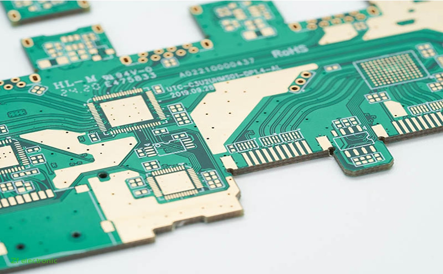
How to choose high temperature PCB material? This blog is mainly about datasheet, types, selection guide, common supplier and cost for high temperature PCB material.
Are you troubled these issues with high temperature PCB?
- High-temp PCBs cracking/delaminating above 150°C?
- Signal distortions in hot-humid environments unsolved?
- Copper migration/insulation failure after long-term heat exposure?
As a professional high temperature PCB manufacturer, EBest Circuit (Best Technology) can provide you service and solutions:
- Custom 200°C+ Materials – Tailored substrates eliminate dielectric loss spikes, ensuring stable signals.
- Stress-Resistant Design – Honeycomb cooling + thermal expansion compensation keeps deformation under 0.1mm at 180°C swings.
- 2000-Hour Aging Validation – Full-cycle testing (heat/cold/humidity) provides traceable reliability data.
- Twenty years of high-temp PCB expertise – solving “can’t use, can’t perform, can’t last” challenges directly.
Feel free to contact us if you have any inquiry for high temperature PCB board: sales@bestpcbs.com.
Why Choose High Temperature PCB Material?
Reasons Why Choose High Temperature PCB Material:
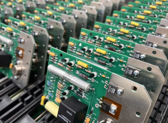
- For extreme operating environments: Equipment requiring long-term operation above 150°C (e.g., automotive engine compartments, spacecraft, oil well drilling equipment) will soften and fail due to the presence of ordinary materials.
- Ensuring structural stability at high temperatures: A high glass transition temperature (Tg≥170°C) prevents PCB deformation and delamination due to heat, avoiding solder joint cracking and component displacement.
- Improving long-term reliability: A low coefficient of thermal expansion (CTE) reduces temperature cycling stress, preventing through-hole copper foil breakage (“barrel cracking”) and extending equipment life (critically used in aerospace and medical equipment).
- Meeting lead-free soldering requirements: Lead-free solder has a high melting point (~217°C), and high-temperature materials (Tg >180°C) can withstand multiple soldering/rework processes without delamination.
- Preventing conductive anode wire (CAF) failure: In high-temperature and high-humidity environments, special resin formulations (e.g., polyimide, modified epoxy) can inhibit short circuits caused by copper ion migration.
- Supports high-power/high-density designs: High-power devices (such as electric vehicle motor controllers) generate localized high temperatures, requiring materials to maintain insulation and mechanical strength within the high-temperature internal layer.
- Accommodates high-frequency/high-speed circuit requirements: Some high-temperature materials (such as PTFE and modified PPO) also possess low dielectric loss (Df), making them suitable for high-frequency applications such as 5G and radar.
- Meets stringent industry certification standards: Automotive (AEC-Q), aerospace (MIL), and industrial applications require mandatory high-temperature reliability testing; specialized materials are a prerequisite for compliance.
High Temperature PCB Material Datasheet
| Parameter | Specification |
| Glass Transition Temperature (Tg) | 130°C, 150°C, 170°C, 180°C, 200°C+ |
| Thermal Decomposition Temperature (Td) | 300°C, 320°C, 340°C, 350°C+ |
| Coefficient of Thermal Expansion (CTE) | X/Y Axis: 12-16 ppm/°C |
| Z Axis | 40-70 ppm/°C |
| Thermal Conductivity | 0.2-0.5 W/(m·K) |
| Water Absorption (24h Immersion) | <0.10%, <0.05% |
| Dielectric Constant (Dk) | 3.5-4.5 (1GHz-10GHz) |
| Dissipation Factor (Df) | 0.002-0.008 (1GHz-10GHz) |
| Soldering Resistance | ≥3 cycles of lead-free reflow soldering (288°C) |
| Peel Strength | ≥0.8 N/mm (copper foil adhesion) |
| Volume Resistivity | >10¹⁴ Ω·cm |
| Surface Resistivity | >10¹³ Ω |
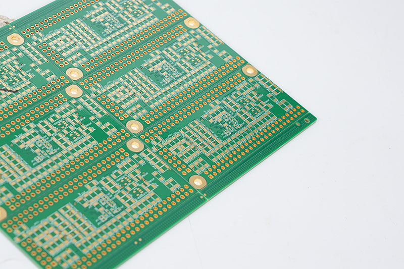
Common High Temperature PCB Materials Types
Polyimide (PI)
- Features: Polyimide is one of the most widely used high-temperature PCB materials, with a glass transition temperature (Tg) typically exceeding 250°C and long-term operating temperatures up to 200°C or higher. It exhibits excellent heat resistance, mechanical strength, flexibility, and resistance to chemical corrosion and radiation.
- Applications: Suitable for high-temperature environments such as aerospace, automotive electronics (e.g., engine control systems), military equipment, and medical instruments. Flexible versions are also applicable to wearable devices.
- Advantages: High reliability, good dimensional stability, but higher costs and greater processing difficulty.
Polytetrafluoroethylene (PTFE)
- Features: PTFE is a high-frequency material with a Tg of approximately 160°C, though it can withstand short-term temperatures up to 260°C. It is renowned for low dielectric constant and low loss factor, ideal for high-frequency and high-speed applications.
- Applications: Primarily used in communication equipment (e.g., 5G base stations), radar systems, and RF modules. For high-temperature environments, it requires combination with reinforcing materials (e.g., ceramic fillers).
- Advantages: Excellent electrical performance and chemical resistance, but poor adhesion, necessitating specialized processing techniques.
Ceramic Substrate Materials (e.g., Al₂O₃ and AlN)
- Features: Ceramic materials offer extremely high thermal conductivity and heat resistance, with operating temperatures exceeding 300°C. Alumina (Al₂O₃) is cost-effective, while aluminum nitride (AlN) provides superior thermal conductivity for high-power density designs.
- Applications: Common in power electronics, LED lighting, electric vehicles, and industrial control systems, used for critical heat-dissipating components.
- Advantages: Outstanding thermal management and mechanical strength, but relatively brittle, requiring careful handling.
Epoxy Resin Composites (e.g., High-Temperature FR-4)
- Features: Standard FR-4 has a Tg of 130-140°C, while high-temperature variants can elevate Tg to 170-180°C by incorporating fillers (e.g., brominated epoxy). It provides good electrical insulation and cost efficiency.
- Applications: Suitable for moderate high-temperature environments in consumer electronics, household appliances, and general industrial equipment, commonly selected for economical high-temperature applications.
- Advantages: Low cost, easy processing, but limited temperature resistance, unsuitable for extreme conditions.
Liquid Crystal Polymer (LCP)
- Features: LCP has a Tg exceeding 280°C, featuring low moisture absorption, high dimensional stability, and exceptional high-frequency performance. It maintains stable performance in high-temperature and high-humidity environments.
- Applications: Mainly used in high-frequency circuits, automotive sensors, and mobile communication devices, particularly suited for miniaturized designs.
- Advantages: Balanced overall performance, suitable for complex environments, but higher raw material costs.
Phenolic Resin-Based Materials
- Features: These materials typically have a Tg of 150-200°C, offering good heat resistance and mechanical hardness, but average electrical performance.
- Applications: Common in older industrial equipment or low-cost applications such as power modules and transformers.
- Advantages: Economical, practical, and readily available, but gradually being replaced by high-performance materials.
How to Choose High Temperature PCB Material?
Below Is A Detailed Selection Guide for High Temperature PCB Material:
1. Clarify Application Scenarios and Temperature Requirements
- Scenario Identification: Precisely define the product operating environment (e.g., automotive engine compartments, aerospace, industrial controls, 5G base stations), as temperature gradients vary significantly across scenarios.
- Temperature Threshold: Determine the maximum continuous operating temperature (e.g., automotive electronics ≥150°C, aerospace up to 300°C+), thermal shock tolerance range (e.g., -55°C to 200°C), and peak soldering temperature (260°C±5°C).
- Lifespan Expectation: Reverse-engineer material long-term thermal stability thresholds based on product design lifespan (e.g., industrial-grade ≥10 years).
2. Match Substrate Type to Temperature-Resistant Parameters
- FR-4 Series: Standard Tg 130-140°C (long-term operation ≤105°C), high-Tg variants ≥170°C (e.g., FR-5, polyimide-reinforced types), suitable for consumer electronics to mid-range industrial scenarios.
- Polyimide (PI): Tg >250°C, withstands extreme environments (-269°C to 300°C), preferred for aerospace flexible circuits, combining dielectric stability and chemical resistance.
- Ceramic Substrates: Alumina (Al₂O₃, thermal conductivity 24W/m·K), aluminum nitride (AlN, 170-230W/m·K), suitable for high-power RF modules and LED heat dissipation, withstanding >300°C.
- Metal Substrates: Aluminum (1-3W/m·K thermal conductivity, cost-effective), copper (200-400W/m·K, high-power scenarios), copper-tungsten alloy (CTE matching semiconductor devices), balancing thermal conductivity and CTE differences.
3. Optimize Coefficient of Thermal Expansion (CTE) Matching
- CTE Discrepancy Risks: FR-4 (12-18ppm/°C) and copper (16-17ppm/°C) have similar CTEs, but high-temperature interlayer stress may cause via fractures and solder joint fatigue.
- Low-CTE Material Selection: High-Tg FR-4 (CTE ≤14ppm/°C), polyimide (10-15ppm/°C), ceramic (4-8ppm/°C), copper-tungsten alloy (6-8ppm/°C), matching semiconductor device CTEs (e.g., SiC 3-6ppm/°C).
- Design Compensation Strategies: Use stepped via structures, symmetric stack layouts, and additional heat-dissipating copper foils to reduce thermal cycling stress concentration.
4. Thermal Conductivity and Heat Dissipation Design
- Thermal Conductivity (W/m·K): FR-4 (0.2-0.4), aluminum (1-3), copper (200-400), ceramic (20-230). High-thermal-conductivity materials require matching heat dissipation path designs.
- Heat Dissipation Optimization: Increase copper layer thickness (≥2oz), implement thermal vias/heat-sink pads, and use thermal interface materials (TIMs), combined with finite element simulation to optimize heat flux density distribution.
5. Validate Dielectric Performance Stability
- Dielectric Constant (Dk) Temperature Coefficient (TCDk): FR-4 TCDk -200 to -400ppm/°C (signal drift risks in high-frequency scenarios). Modified materials like Rogers RO4350B (TCDk +50ppm/°C) and Taconic TLY-5 (TCDk +10ppm/°C) offer greater stability.
- Testing and Compensation: Measure Dk temperature characteristics via resonant cavity/transmission line methods. Design with impedance matching allowances. High-frequency circuits may require dynamic compensation algorithms (e.g., clock delay adjustment).
6. Chemical Resistance and Environmental Adaptability
- Chemical Corrosion Resistance: Polyimide and ceramic substrates resist acid/base and solvent corrosion. FR-4 requires compatibility evaluation with conformal coatings to avoid CAF (cathodic anode filament) short-circuit risks.
- Moisture and Humidity Resistance: Low-moisture-absorption materials (e.g., ceramic <0.1%), hermetic packaging designs, and validation of insulation performance via damp heat tests (85°C/85% RH). Salt spray corrosion resistance is critical for marine environments.
7. Certification Standards and Compliance Verification
- International Certifications: UL certification (flammability ratings), RoHS/REACH (environmental compliance), IPC Class 2/3 (reliability grades), industry-specific standards like IATF 16949 (automotive) and AS9100 (aerospace).
- Testing and Traceability: 100% electrical performance testing, thermal cycling/vibration impact testing, and accelerated life testing (HALT/HASS). Raw material traceability systems ensure batch consistency. Suppliers must be certified to ISO 9001/14001 standards.
Common High Temperature PCB Material Suppliers
1. Rogers Corporation
Advantages
- Glass transition temperature (Tg) up to 280°C (e.g., RO4350B, RO4003C), with long-term operating temperatures exceeding 200°C.
- Low dielectric loss (Df as low as 0.0037) and stable dielectric constant, ideal for high-frequency/microwave circuits.
- High thermal conductivity (0.5–2 W/m·K) and low coefficient of thermal expansion (CTE), enhancing dimensional stability in high-temperature environments.
Business
- Full range of high-frequency laminates, prepregs, and custom materials (e.g., RO3000, RO4000, TMM® series).
- Serves premium markets including 5G base stations, aerospace, automotive radar, and high-speed digital equipment.
2. Isola Group
Advantages
- Tg ranges from 180–260°C (e.g., 370HR Tg=180°C, P95/P25 Tg=260°C), with decomposition temperatures up to 380°C.
- Excellent CAF resistance and low Z-axis thermal expansion (Z-CTE ≤45 ppm/°C).
- Halogen-free options compliant with RoHS, suitable for environmentally regulated applications.
Business
- Epoxy and polyimide laminates/prepregs spanning medium-to-high loss (e.g., FR406, 370HR, I-SPEED®, Tachyon® 100G).
- Focuses on automotive electronics, servers, industrial controls, and high-speed digital communication devices.
3. Panasonic (MEGTRON Series
Advantages
- MEGTRON7 R-5785 achieves Tg of 200°C; MEGTRON6 R-5775 reaches 205°C (TMA method).
- Ultra-low dielectric constant (Dk≈3.4–3.8) and loss factor (Df≤0.003), optimized for 5G/millimeter-wave applications.
- High thermal resistance (Td>300°C) and robust insulation reliability for multi-layer (20+ layer) PCBs.
Business
- MEGTRON2–MEGTRON8 high-speed/high-frequency laminates and prepregs.
- Deployed in routers, servers, mobile base stations, and automotive radar systems requiring high temperature and reliability.
4. Shengyi Technology
Advantages
- High-Tg portfolio: SI10US Tg=280°C, S1000-2 Tg=170°C, S7439G Tg=189°C.
- Low moisture absorption (≤0.1%) and superior CAF resistance for enhanced humidity/thermal reliability.
- Halogen-free designs compatible with lead-free soldering processes.
Business
- Product lines include standard FR-4, mid-high-speed materials (Synamic series), and polyimide substrates (e.g., SH260 Tg>250°C).
- Widely used in computing, telecommunications, automotive electronics, and consumer electronics.
5. Kingboard (Jian Tao Laminates)
Advantages
- KB-6164 Tg=140°C with robust thermal performance and CAF resistance, meeting IPC-4101D/27 standards.
- Cost-effective solutions competitive in mid-tier high-temperature applications.
- Diverse options including yellow/white CEM-1 composite substrates and black FR-4.
Business
- Supplies conventional and mid-performance laminates (FR-4, CEM-1, CEM-3).
- Clients span consumer electronics, power equipment, and industrial control sectors.
How to Select A Reliable High Temperature PCB Material Supplier?
1. Define Core Performance Parameters for High-Temperature PCB Materials
- Ensure precise matching of temperature resistance grades (e.g., Tg ≥ 180°C, Td ≥ 320°C, CTE ≤ 20ppm/℃) based on application scenarios (e.g., automotive engine compartments, aerospace).
- Validate long-term thermal aging performance through accelerated aging tests (e.g., ≤3% dielectric constant variation, ≥90% insulation resistance retention after 1000 hours at 150°C).
2. Verify Supplier Quality Certifications and Compliance
- Prioritize suppliers with international certifications such as ISO 9001, IATF 16949 (automotive), AS 9100 (aerospace), and UL 94 V-0 (flame retardancy) to meet target market regulations.
- Require third-party test reports from SGS or TÜV Rheinland covering RoHS, REACH, HF compliance, and complete thermal/electrical/mechanical performance data.
3. Assess Customized Technical Support Capabilities
- Evaluate the supplier’s ability to develop customized material formulations (e.g., high-frequency, chemical-resistant, ultra-thin substrates) and provide samples for validation.
- Ensure process compatibility support, including optimized lamination temperature profiles, drilling parameters, and surface treatment processes.
4. Ensure Supply Chain Stability and Delivery Guarantees
- Select suppliers with global logistics networks and local technical teams supporting trade terms like DDU/DDP, ensuring 7-14 day lead times and reduced international shipping risks.
- Review inventory management systems and emergency response plans for urgent orders (e.g., 48-hour expedited delivery).
5. Validate Customer References and Reputation
- Request case studies from automotive (e.g., Bosch, Continental), aerospace (e.g., Airbus, Boeing), and industrial control (e.g., Siemens, ABB) sectors, along with backdoor reference contacts.
- Check independent reviews on platforms like Trustpilot or Google Reviews for quality consistency, technical response speed, and after-sales service quality.
6. Optimize Cost Efficiency and Long-Term Partnership Strategies
- Demand transparent pricing (material costs, processing fees, logistics) and negotiate tiered pricing/annual rebates via long-term contracts.
- Prioritize ESG-compliant partners with carbon footprint management, waste reduction practices, and sustainable supply chain initiatives to enhance corporate image.
7. Emphasize Environmental and Sustainability Practices
- Choose suppliers using halogen-free, recyclable substrates compliant with EU ELV/WEEE directives to minimize lifecycle environmental impact.
- Require carbon footprint reports and support carbon reduction through optimized packaging/logistics (e.g., sea freight over air freight) to align with client decarbonization goals.
How Much Does High Temperature PCB Materials Cost?
Specialty Copper Clad Laminates
- High-Frequency, High-Speed Copper Clad Laminates (e.g., Rogers series): $300 – $800/㎡ (Depending on dielectric constant and loss factor grades).
- Ceramic-Based Copper Clad Laminates (High Thermal Conductivity): $180 – $500/㎡ (Alumina-based substrates are cheaper; aluminum nitride substrates can reach $450+/㎡).
- High-Temperature Copper Foil (300℃+): $25 – $50/kg (For extreme environments such as all-solid-state batteries).
Resin Systems
- Polyimide Resin (PI): $120 – $300/kg (ESA certified VT-901PI and other models are 30% more expensive).
- High-Heat-Resistant Epoxy Resin (M9 grade): $80 – $150/kg (Domestic alternatives are 20%-30% cheaper).
Conformal Coating Materials:
- Silicone-based: $40 – $80/L (High temperature resistance >200℃).
- Polyurethane-based: $20 – Acrylic resin: $7 – $10/L (including solvent) $35/L.
Welcome to contact us if you need any help for high temperature PCB materials: sales@bestpcbs.com.