High speed PCB design Radiocord technologies refers to advanced printed circuit board engineering techniques used to ensure stable signal transmission at high data rates and fast edge speeds. This article explains what defines a high-speed PCB, the frequencies that require high-speed design rules, suitable materials like FR-4, impedance control requirements, stack-up strategies, crosstalk mitigation, simulation tools, and practical design workflows.
What Is Considered a High Speed PCB?
A PCB is considered high speed when signal timing and electromagnetic behavior begin to affect circuit performance. At lower speeds, traces behave like simple conductors. As signal edges become faster, traces begin acting like transmission lines.
Many engineers evaluate this change using signal rise time. When the signal edge becomes very short, electromagnetic effects become more significant.
A common estimation formula is:
Bandwidth ≈ 0.35 / Rise Time
For example:
| Rise Time | Approximate Frequency Content |
| 5 ns | ~70 MHz |
| 1 ns | ~350 MHz |
| 500 ps | ~700 MHz |
| 100 ps | ~3.5 GHz |
Today, many electronic systems require high speed PCB design, including:
- Data center servers
- High-performance computing platforms
- Networking switches and routers
- Automotive radar electronics
- Medical imaging equipment
Modern processors often communicate with memory at speeds exceeding 20–30 Gbps per lane, which requires strict signal integrity control in PCB layout.

What Frequency Requires High Speed PCB Design?
There is no single frequency that defines a high speed PCB. However, many engineers begin applying high speed design rules when signal frequencies exceed 50 MHz to 100 MHz.
Above this range, several signal integrity challenges begin to appear:
- Signal reflections
- Crosstalk between traces
- Timing distortion
- Electromagnetic interference
Modern digital interfaces operate far beyond this range.
| Interface | Data Rate |
| USB 3.0 | 5 Gbps |
| PCIe Gen4 | 16 GT/s |
| PCIe Gen5 | 32 GT/s |
| 10 Gigabit Ethernet | 10 Gbps |
These speeds introduce frequency components in the gigahertz range. According to industry research from Cisco’s Global Cloud Index, global data center traffic has exceeded 20 zettabytes annually, and modern network links commonly operate at 25 Gbps, 56 Gbps, and even 112 Gbps per channel.
Can FR4 Be Used for High Speed PCB?
FR4 remains the most commonly used PCB substrate in the electronics industry. It offers good mechanical strength, wide availability, and relatively low manufacturing cost.
Typical FR4 properties include:
- Dielectric constant: 4.2 – 4.6
- Loss tangent: ~0.015 at 1 GHz
- Glass transition temperature: 130–170°C
FR4 works well for many digital systems, including:
- Computer motherboards
- Industrial control boards
- Consumer electronics
- Networking equipment
However, signal loss increases as operating frequency rises. When data rates exceed 10 Gbps, engineers sometimes choose lower-loss laminates to maintain signal quality.
Common high-speed materials include:
- Rogers laminates
- Megtron series materials
- Nelco high-speed laminates
Even so, many systems still use FR4 successfully when trace lengths are controlled and stackup design is optimized.
What Impedance Is Used in High Speed PCB?
Controlled impedance is critical in high speed PCB design. It ensures that signals travel along traces without reflections.
When impedance changes along a signal path, part of the signal reflects back toward the source. This reflection can distort digital signals and create timing errors.
Common impedance targets include:
| Signal Type | Impedance |
| Single-ended signals | 50 Ω |
| Differential pairs (Ethernet) | 100 Ω |
| USB differential pairs | 90 Ω |
| PCIe differential pairs | 85 Ω |
Several factors determine trace impedance:
- Trace width
- Dielectric thickness
- Copper thickness
- Distance to the reference plane
Most high-speed designs require impedance tolerance within ±10%, while more sensitive systems may require ±5% control.
PCB manufacturers verify impedance using Time Domain Reflectometry (TDR) testing to ensure the finished board meets electrical specifications.
What Stackup Is Best for High Speed PCB?
Stackup design strongly influences signal integrity and electromagnetic compatibility. A well-designed stackup provides stable reference planes and controlled impedance for high-speed signals.
A typical 6-layer high-speed PCB stackup looks like this:
| Layer | Function |
| Layer 1 | Signal |
| Layer 2 | Ground plane |
| Layer 3 | Signal |
| Layer 4 | Power plane |
| Layer 5 | Ground plane |
| Layer 6 | Signal |
This configuration offers several advantages:
- Stable return paths for high-speed signals
- Reduced electromagnetic interference
- Improved impedance consistency
- Better power distribution stability
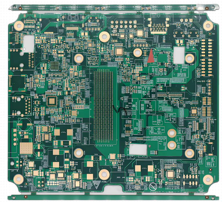
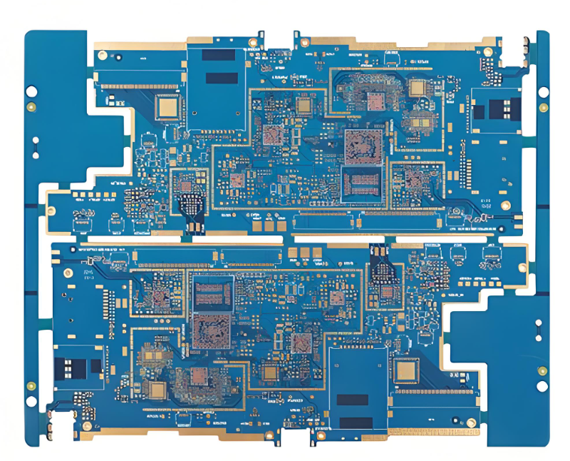
More complex digital systems often require 8 to 12 layers. High-performance computing boards sometimes exceed 20 layers to support dense routing and multiple signal channels.
How Do You Reduce Crosstalk in High Speed PCB?
Crosstalk occurs when electromagnetic energy from one signal trace couples into another nearby trace. This interference can introduce noise and reduce signal reliability. Crosstalk becomes stronger when traces run parallel over long distances.
Several layout techniques help reduce crosstalk:
- Increase spacing between adjacent signal traces
- Avoid long parallel routing segments
- Route adjacent layers at 90-degree angles
- Place signal layers close to ground planes
- Use differential pair routing
A common design guideline recommends spacing of at least three times the trace width.
For example, if a trace is 5 mil wide, the spacing should ideally be 15 mil or greater. These layout strategies help maintain stable signal performance in dense PCB designs.
What Simulation Tools Are Used for High Speed PCB?
Simulation tools allow engineers to evaluate signal behavior before manufacturing begins. These tools model electromagnetic effects such as reflections, signal loss, and crosstalk.
Common high-speed simulation tools include:
- Cadence Sigrity
- ANSYS HFSS
- Keysight ADS
- Mentor HyperLynx
- Altium Designer signal integrity tools
These platforms help engineers analyze several critical parameters:
- Eye diagram quality
- Signal reflections
- Crosstalk levels
- Power distribution noise
For example, a 10 Gbps communication channel must maintain a clear eye opening to ensure reliable data transmission. Early simulation helps identify potential problems before fabrication begins.
How to Design a High-Speed PCB?
Designing a high-speed PCB requires careful planning and a structured workflow. Each design step helps maintain signal integrity across the circuit board.
A typical design process includes:
- Define system speed and interface requirements
- Select appropriate PCB materials
- Plan the multilayer stackup
- Route critical high-speed signals first
- Maintain controlled impedance routing
- Minimize unnecessary vias
- Match differential pair lengths
- Perform signal integrity simulation
- Build prototypes for validation
- Prepare the design for production
Typical High-Speed PCB Design Parameters
| Parameter | Typical Value |
| Differential impedance | 85–100 Ω |
| Single-ended impedance | 50 Ω |
| Trace width (common) | 3–6 mil |
| Minimum spacing | 3× trace width |
| Via stub length | < 10 mil |
| Signal rise time | < 1 ns for high-speed systems |
These parameters are widely used in high-speed digital systems such as Ethernet switches, GPU boards, and high-performance servers.
What Is the Difference Between High Speed and High-Frequency PCB?
The terms high speed PCB and high-frequency PCB are often used interchangeably, but they focus on different engineering challenges. High speed PCBs mainly deal with fast digital signals and timing accuracy, while high-frequency PCBs are designed for analog RF or microwave signals that operate at very high frequencies.
The comparison below highlights the key distinctions.
| Feature | High Speed PCB | High-Frequency PCB |
| Signal Type | Digital signals with fast switching edges | Analog RF or microwave signals |
| Main Design Focus | Signal integrity and timing control | Electromagnetic wave behavior |
| Typical Frequency Range | Tens of MHz to several GHz | Usually above 1 GHz |
| Key Challenge | Reflections, crosstalk, and timing skew | Signal loss, radiation, and impedance matching |
| Trace Behavior | Transmission line effects due to fast edges | Full RF transmission behavior |
| Material Requirements | FR4 often usable for many designs | Usually requires low-loss RF materials |
| Typical Materials | FR4, high-speed digital laminates | Rogers, PTFE, ceramic-filled substrates |
| Impedance Control | Important for digital interfaces | Critical for RF signal matching |
| Common Applications | Servers, networking hardware, computer motherboards | Radar systems, wireless communication, satellite electronics |
| Design Tools | Signal integrity simulators | RF electromagnetic simulation tools |
| Layout Considerations | Differential pairs, length matching, return paths | RF shielding, impedance matching networks |
In high speed digital circuits, engineers mainly worry about signal edges and timing alignment. Even when the base frequency is moderate, the fast rise time of digital signals creates high-frequency components that require careful routing.
In contrast, high-frequency circuits operate directly in the RF or microwave domain. Engineers must consider wave propagation, radiation, antenna effects, and impedance matching across the entire signal path.
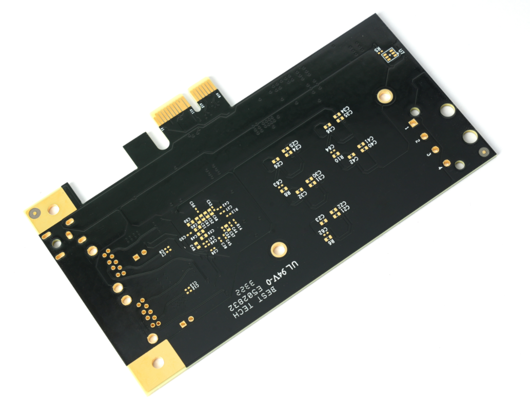
Why Choose Best Technology as Your High Speed PCB Manufacturer?
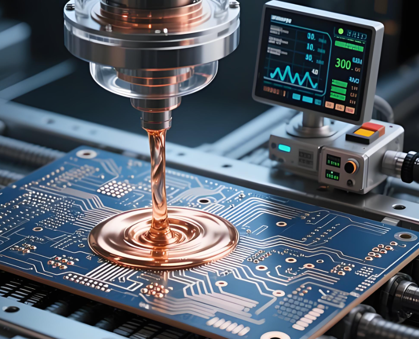
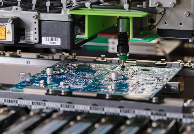
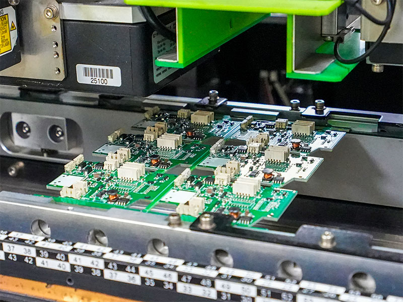
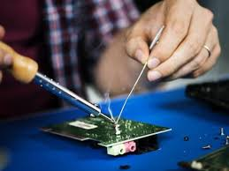
High-speed PCB fabrication requires precise manufacturing control. Even small variations in trace width or dielectric thickness can affect impedance and signal integrity.
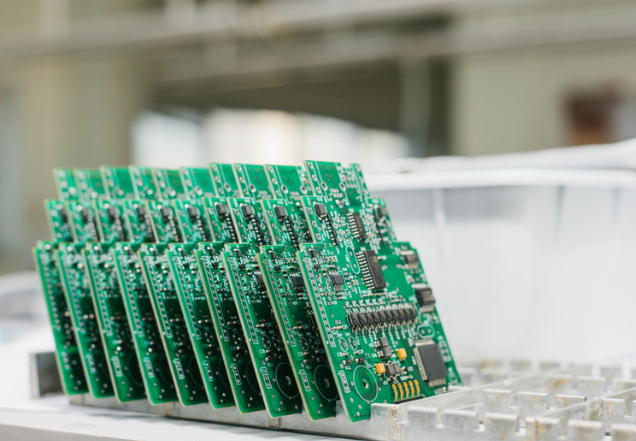
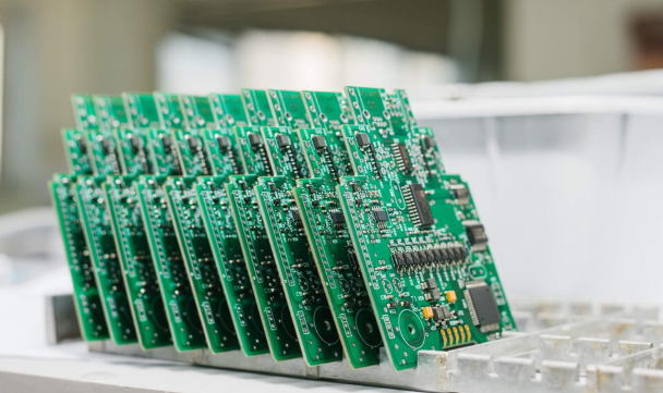
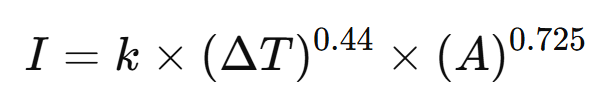
Best Technology has developed extensive experience in multilayer PCB manufacturing for communication systems, computing hardware, and industrial electronics. Their fabrication processes support controlled impedance routing and complex stackup structures.
Key technical capabilities include:
- Multilayer PCB production up to 30 layers
- Controlled impedance tolerance within ±5%
- Support for advanced high-speed laminates
- Fine trace width and spacing down to 3 mil
- Electrical verification using TDR impedance testing
Working with an experienced manufacturer during the design stage can help ensure the final PCB meets both electrical and manufacturing requirements.
For technical inquiries or PCB manufacturing support, please contact: sales@bestpcbs.com