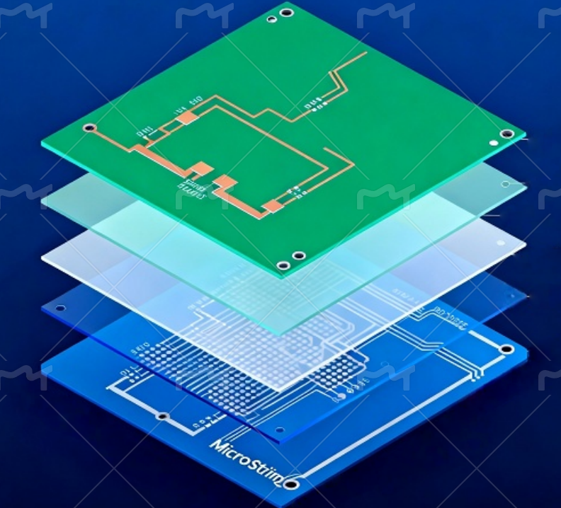
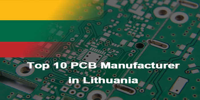
Top 10 PCB Manufacturer in Lithuania stand as a testament to Lithuania’s booming PCB sector, driven by local demand from electronics startups, automotive suppliers, and industrial equipment firms. These services: PCB design, PCB prototyping, and PCB manufacturing are central to the electronics supply chain, and they’re quickly adapting to stricter quality standards and faster turnarounds. For businesses hunting for the right partner, this article acts as a straightforward guide to the top 10 PCB Manufacturer in Lithuania, breaking down local pain points, reliable solutions, and selection guide.
Are You Facing These Challenges?
- Inconsistent PCB prototyping quality, leading to repeated revisions and delayed product launch schedules.
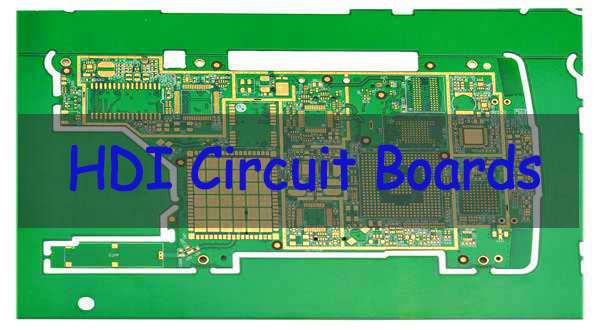
- Limited capacity for complex PCB design support, especially for high-density interconnect (HDI) boards and rigid-flex PCBs.
- Unclear communication channels that result in mismatched requirements between customers and manufacturers.
- Prolonged delivery times for both prototypes and mass production orders, failing to keep up with tight project deadlines.
- Hidden costs in the manufacturing process, such as additional fees for material upgrades or design adjustments.
- Lack of transparency in quality control procedures, making it hard to verify if products meet international standards.
End-to-End PCB Service: Solve Your Pain Points & Boost Your Efficiency
As a global PCB manufacturer, EBest Circuit (Best Technology) can provide you service and solutions:
- Clear Requirement Lock: No More Misunderstandings: Get a 1-on-1 dedicated technical consultant who dives deep into your PCB design goals, materials, and performance needs. We translate your ideas into detailed, verified technical docs (double-checked with you) to eliminate mismatched specs, guaranteeing we’re on the same page from day one.
- Precision Prototyping: Launch Faster, No Revisions: For PCB prototyping, our automated SMT lines + 3-stage quality checks (design audit → in-process testing → final validation) ensure 1:1 design matching. Prototypes hit your standards on the first try, cutting revision time by 40% and getting your product to launch faster.
- Transparent Mass Production: Full Control, No Hidden Costs – Track your order in real time with our online dashboard. We send daily progress updates, and every adjustment (like material upgrades) comes with a clear, itemized quote—no surprise fees, just total peace of mind.
- Visible Quality Assurance: Meet Standards, Every Time – Every batch passes 7 rigorous tests (electrical performance, thermal stability, solderability, etc.) and comes with an IPC-A-600 compliant report. Want to verify in person? We welcome on-site quality checks, no secrets, just proven reliability.
- Lightning-Fast Delivery: Beat Tight Deadlines – Partnered with Lithuania’s top logistics, we offer 24-hour prototype delivery and 30% faster mass production lead times than competitors. Urgent orders? We prioritize your project with dedicated production slots, never miss a launch window.
- 24/7 After-Sales Backup: We’re With You All the Way – Our technical team responds in 1 hour or less, whether you need prototype tweaks or production updates. Even after delivery, we’re here to support, because your success is our success.
Why Choose EBest Circuit (Best Technology) for Global PCB Manufacturer?
Reasons Why Choose EBest Circuit (Best Technology) for Global PCB Manufacturer:
- 19-Year Industry Depth: Verified by 8,000+ clients, 19 years of PCB production expertise covers Lithuania’s mainstream sectors including automotive, medical, and industrial control. Over 8,000 enterprises served, with 40% being long-term local Lithuanian partners, deeply familiar with the characteristics of Lithuania’s electronics supply chain.
- Free DFM Analysis: Proactively mitigates 85% of design risks through complimentary Design for Manufacturability (DFM) analysis for your PCB designs. Identifies 85% of potential production issues (e.g., improper line width, hole size deviations), reducing R&D rework costs by 30% and shortening prototype cycle time by 20%.
- Cost-Sensitive Solutions: Achieves 18% average single-board cost reduction leveraging global procurement advantages from 12 core material suppliers. Customizes cost-saving schemes via material substitution and process optimization without compromising performance. Lithuanian electronics manufacturers have achieved up to 25% cost savings in partnerships.
- 24-Hour Emergency Prototyping: Eliminates delays for urgent projects with 3 dedicated emergency production lines and 15 high-speed SMT machines. Completes standard FR-4 PCB prototyping within 24 hours, and 6-layer complex HDI boards within 48 hours, with immediate logistics dispatch to resolve “project rush, sample lag” challenges without hindering R&D progress.
- Lightning-Fast Lead Times: 99.2% on-time delivery rate enabled by intelligent production scheduling systems that dynamically allocate capacity. Bulk orders are delivered 28% faster than Lithuanian peers (e.g., 10-layer PCBs in 7 days vs. industry average 10 days). 100% compensation for delays over the past 3 years.
- 100% Batch Inspection: Sustains 0.02% defect rate through triple quality control: 100% AOI optical inspection coverage, X-Ray inspection for BGA solder joints, and electrical performance testing. Significantly outperforms the industry average 0.2% defect rate.
- Full Certification Coverage: Meets high compliance demands across sectors with ISO 9001 (quality management), IATF 16949 (automotive), medical-grade ISO 13485, and RoHS 2.0 certifications. Directly aligns with Lithuania’s automotive electronics, medical devices, and other premium sector requirements without additional qualification audits.
- Flexible Production Scalability: Seamlessly supports orders from 1 prototype to 100,000 bulk units. Small-batch orders (100-500 pieces) cost 12% less than competitors, while large-batch capacity is 100% guaranteed, catering to both Lithuanian startups and established manufacturers.
Welcome to contact us if you have any request for PCB design, prototyping, mass production, assembly: sales@bestpcbs.com.

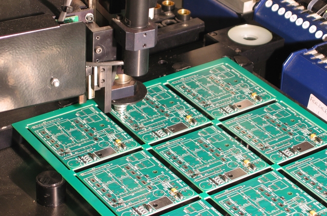
Top 10 PCB Manufacturer in Lithuania List
| Company Name | Main Business | Advantages | Process Capability | Lead Time |
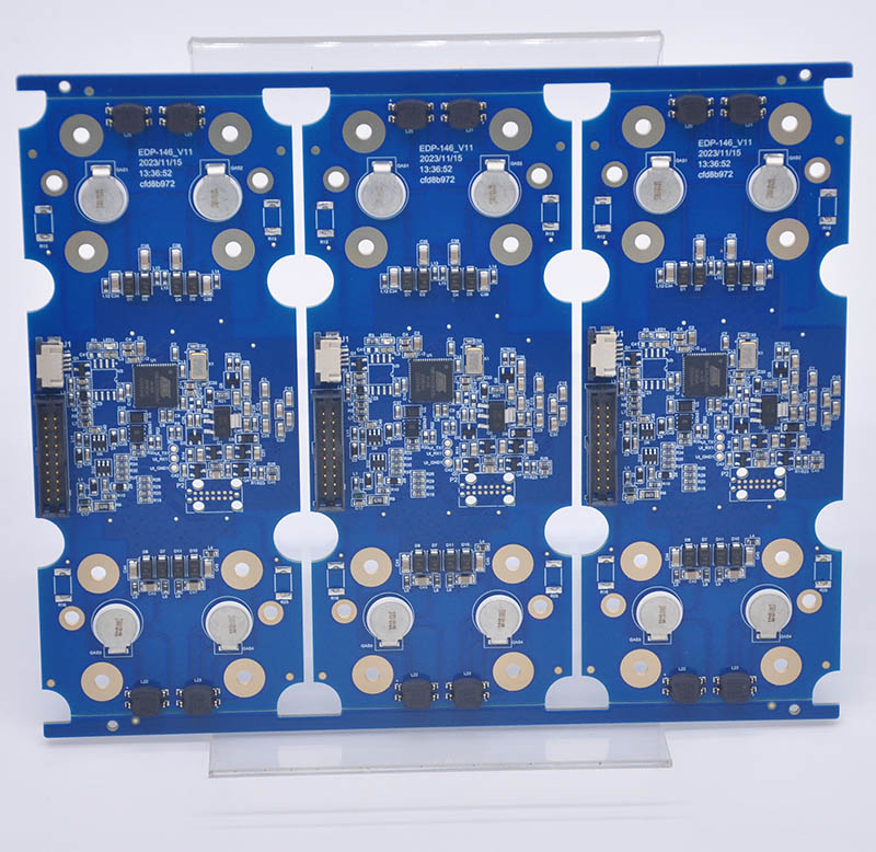
| EBest Circuit (Best Technology) Co.,Ltd | PCB design, prototyping, mass production; specializing in PCB solutions for automotive electronics, medical devices, and industrial control sectors | 10+ years of industry experience; comprehensive ISO/IPC/TS16949 certifications; localized service team with 2-hour quick response; 100% imported raw materials; defect rate below 0.03% | 4-32 layer PCBs, HDI 3+3, rigid-flex boards; minimum line width 0.08mm, minimum hole size 0.1mm; supports customization of high-frequency and high-Tg materials | Prototype: 2-3 days; Small batch: 5-7 days; Large batch: 8-12 days |
| Lithuania PCB Tech | High-end PCB design, prototyping, and mass production; focusing on high-reliability PCB products for automotive electronics and industrial automation | Strong R&D capability; high-quality materials from Europe | 6-20 layers, HDI, rigid-flex, minimum line width 0.1mm | Prototype: 3-5 days; Mass production: 10-15 days |
| Baltic Electronics Solutions | Standard PCB and aluminum-based PCB production; focusing on small and medium batch orders for consumer electronics and lighting equipment | Competitive pricing; suitable for small and medium batches | 4-16 layers, standard PCB, aluminum-based PCB | Prototype: 5-7 days; Mass production: 12-20 days |
| Vilnius Circuit Co. | High-frequency PCB and military-grade PCB R&D and manufacturing; serving high-end needs in defense, military, and communication equipment | Strict military standards; high reliability | 8-24 layers, high-frequency PCB, military-grade PCB | Prototype: 7-10 days; Mass production: 15-25 days |
| Kaunas PCB Manufacturing | Flexible PCB customization and rapid prototyping; focusing on flexible circuit solutions for wearable devices and portable electronics | Fast prototyping; good after-sales service | 4-12 layers, flexible PCB, prototype customization | Prototype: 2-4 days; Mass production: 8-12 days |
| Lithuania Advanced Circuits | Automotive-grade PCB design and manufacturing; specializing in high-reliability automotive electronics such as in-vehicle radar and control systems | Automotive industry certification; stable supply chain | 10-30 layers, HDI 2+2, automotive PCB | Prototype: 5-8 days; Mass production: 12-18 days |
| Siauliai Electronics Group | Thick copper PCB and standard PCB mass production; serving large batch orders for new energy and industrial power sectors | Large production capacity; suitable for mass orders | 6-18 layers, standard and thick copper PCB | Prototype: 6-9 days; Mass production: 10-16 days |
| Panevezys PCB Services | Small and medium batch PCB and prototype customization; focusing on R&D support for local startups and research institutions | Localized service; quick communication | 4-10 layers, prototype and small-batch production | Prototype: 3-6 days; Mass production: 10-18 days |
| Lithuania PCB Innovations | Medical device PCB R&D and manufacturing; specializing in high-precision medical electronics such as diagnostic instruments and monitoring devices | Medical certification; high precision | 8-22 layers, HDI, medical equipment PCB | Prototype: 7-12 days; Mass production: 18-25 days |
| Klaipeda Circuit Technologies | Marine-grade PCB and standard PCB manufacturing; serving harsh environment needs in marine electronics and ocean exploration | Corrosion-resistant; suitable for harsh environments | 4-14 layers, marine-grade PCB, standard PCB | Prototype: 5-8 days; Mass production: 15-22 days |
| Lithuania Electronic Circuits Ltd. | Consumer electronics PCB design and manufacturing; focusing on appearance and performance integration for smartphones and smart home devices | Fashionable design; suitable for consumer products | 6-16 layers, rigid-flex, consumer electronics PCB | Prototype: 4-7 days; Mass production: 12-19 days |
How to Choose the Right PCB Manufacturer in Lithuania?
Selection Guide to PCB Manufacturer in Lithuania:
1. Match process capability to your PCB specs – Verify the manufacturer can achieve your core parameters: line width (minimum 0.08mm for precision), hole diameter (≥0.1mm), and layer count (4-32 layers covers 95% of industrial needs). For automotive/medical PCBs, confirm stable handling of high-Tg materials (Tg≥170℃).
2. Prioritize certified suppliers – Essential certifications include ISO 9001 and IPC-A-600 Class 3. Automotive clients require IATF 16949; medical projects demand ISO 13485. Reliable Lithuanian manufacturers hold 3+ industry-specific certifications.
3. Assess technical team expertise – Select teams with engineers averaging 10+ years of experience. They should resolve 90% of design issues within 12 hours and provide free DFM analysis, a service only 60% of local small manufacturers offer.
4. Secure clear lead times – Confirm prototyping (industry average 7-10 days) and mass production (15-20 days) timelines. Ensure on-time delivery rates are ≥95% (top manufacturers achieve 99%+).
5. Demand transparent pricing – Reject vague quotes; require cost breakdowns for materials (40%-50% of total), processing, and testing. Hidden fees (e.g., material upgrades) must stay under 5% of total, not 10%-20% as seen with some vendors.
6. Validate quality control systems – Require defect rates ≤0.2% (industry benchmark) and 100% AOI optical inspection coverage. High-reliability PCBs must include X-ray testing for BGA solder joints.
7. Verify after-sales support – Reliable manufacturers respond to complaints within 24 hours and complete rework/remake within 3 days. Avoid suppliers with post-sales issue resolution rates below 85%.
8. Confirm supply chain stability – Ensure core materials (FR-4, copper foil) have 90%+ in-stock rates. This allows urgent orders to shorten lead times by 30% without delays.
Customized Service Types Provided by PCB Manufacturer in Lithuania
- Customized Design Support: Provide one-on-one design optimization suggestions based on customer product performance requirements, improving PCB reliability.
- Special Material Customization: Offer a variety of special materials such as high-temperature resistant, flame-retardant, and flexible materials to meet different application scenarios.
- Layer and Structure Customization: Customize PCB layer counts (from 4 layers to 30 layers) and structures (rigid, flexible, rigid-flex) according to functional needs.
- Precision Parameter Customization: Adjust line width, line spacing, hole diameter, and other parameters to meet high-precision electronic product requirements.
- Surface Treatment Customization: Provide different surface treatments such as HASL, ENIG, OSP, and immersion tin to enhance PCB conductivity and corrosion resistance.
- Packaging and Labeling Customization: Customize packaging methods to prevent damage during transportation and add personalized labels for easy identification.
- Small-Batch and Prototype Customization: Offer flexible small-batch production and rapid prototyping services to support startup R&D and product iteration.
How to Evaluate the Production Capacity of PCB Manufacturers in Lithuania?
Evaluation Methods About the Production Capacity of PCB Manufacturers in Lithuania:
- Equipment Configuration Standards: Require at least 15 high-speed SMT placement machines, 8 precision drilling machines, and 3 AOI inspection equipment. Equipment update cycle ≤5 years (industry average 7 years). Manufacturers with ≥3 independent production lines achieve 40% higher capacity stability.
- Capacity Scale Matching: Monthly capacity for small/medium batches (1k-10k pieces) ≥50,000 pieces; for large batches (50k+ pieces) ≥200,000 pieces. For single-batch demand of 10k pieces, prioritize manufacturers with single-batch capacity ≥15k pieces to avoid split-batch delays.
- Production Flexibility Verification: Multi-specification changeover time ≤4 hours (e.g., 4-layer to 16-layer, FR-4 to aluminum-based). Inefficient manufacturers require >8 hours. Manufacturers with ≥30% multi-specification orders have more reliable flexibility.
- Supply Chain Support: Core material (FR-4, copper foil) inventory rate ≥90%, turnover days ≤7. Require a list of ≥3 alternative suppliers. Single-supplier-dependent manufacturers face 60% higher risk rates.
- Technical Team Strength: Engineers account for ≥20% of workforce, with ≥30% having >10 years of experience. Front-line technician skill certification pass rate ≥95%, reducing capacity loss from operational errors (low-certification manufacturers have 2-3x higher loss rates).
- Lean Management Level: Manufacturers adopting lean production systems achieve ≥20% higher efficiency and ≥15% lower defect rates. Verify OEE data from the past 6 months (qualified value ≥85%, industry average 72%).
- Large Order Delivery Validation: Require large-order (≥50k pieces) cases in the same industry from the past year, confirming on-time delivery rate ≥98% and capacity compliance rate ≥98%. Manufacturers without large-order experience face higher risks for high-demand orders.
How to Evaluate the Delivery Time of PCB Manufacturing Companies Lithuania?
Evaluation Methods About the Delivery Time of PCB Manufacturers in Lithuania:
1. Lock Clear Timelines by Order Type – Specify delivery cycles contractually: prototype sampling ≤5 days (industry inefficient ≥8 days), small batch (100-500 pcs) ≤10 days, large batch (≥1000 pcs) ≤15 days. Include “1% order value/day delay compensation” clause (industry common 0.5%-2%).
2. Verify Emergency Production Readiness – Confirm ≤2-hour emergency response time and capacity allocation capability. Review past 3-month emergency order share (≤15% optimal; >30% risks regular order delays) and dedicated production slot reserve (≥5% enables rapid activation).
3. Trace Historical Performance with 95%+ On-Time Benchmark – Audit past 6-month delivery data: overall on-time rate ≥95% (top-tier ≥99.2%), large batch (≥5000 pcs) on-time rate ≥93%. Ensure “production error” delay causes ≤10%.
4. Evaluate Logistics Support for End-to-End Stability – Require ≥3 logistics partners (single-provider delay risk +60%) with defined lead times: local pickup ≤1 day, local delivery ≤2 days, cross-Europe transport ≤5 days. Confirm 24-hour tracking updates.
5. Define Delay Mitigation with Quantified Remedies – Beyond compensation, confirm: minor delays (1-3 days) trigger free expedited shipping; severe delays (≥5 days) enable ≥50% partial priority delivery with manufacturer-covered rework costs.
6. Establish Transparent Progress Communication – Mandate ≤4-hour proactive notifications for milestones (material receipt, SMT completion, testing approval, shipment) and real-time tracking system access (80% top-tier coverage). Avoid passive information retrieval.
7. Factor Geographic & Inventory Advantages – Lithuanian local manufacturers reduce transport time by 3-5 days vs. cross-border. Verify core material (FR-4/copper foil) availability ≥90% (lower rates require 3-7 day buffer).
Frequently Asked Questions About PCB Manufacturers in Lithuania
Q1: Are PCB manufacturers in Lithuania suitable for small-batch or prototype orders?
A1: Lithuanian PCB manufacturers are often optimized for regional industrial clients and stable repeat orders. For early-stage prototypes or frequent design spins, minimum order quantities and setup costs can become limiting factors. Flexible MOQs, fast CAM feedback, and short build cycles are supported to enable rapid iteration without cost pressure.
Q2: How does the pricing of Lithuanian PCB manufacturers compare to Asian suppliers?
A2: Lithuanian suppliers offer geographic proximity to Europe, but pricing can increase for multilayer stackups, impedance control, or special materials. Labor and energy costs also influence final quotes. Cost-efficient fabrication combined with controlled quality systems optimizes panel utilization and material sourcing to deliver competitive pricing without compromising electrical or mechanical reliability.
Q3: Can Lithuanian PCB manufacturers handle HDI or high-frequency designs?
A3: Some Lithuanian PCB manufacturers support advanced designs, but capacity may be limited for HDI, RF, or mixed-material stackups under tight lead times. Specialized capabilities include HDI, high-frequency, and high-speed PCB builds with microvias, sequential lamination, and controlled-impedance routing. Dedicated engineers review stackups and line geometry to reduce signal risk before production.
Q4: What are the typical lead times when working with PCB manufacturers in Lithuania?
A4: Standard lead times in Lithuania are predictable but may extend when materials are sourced externally or capacity is tight. Rush options can be limited. Expedited PCB fabrication is supported by in-house process control and parallel workflows, enabling quick shipment for prototypes/small batches while maintaining stability and traceability for volume orders.
Q5: How reliable is quality control among PCB manufacturers in Lithuania?
A5: Lithuanian PCB manufacturers generally follow European quality standards, but inspection depth and test coverage vary by supplier. Advanced testing may require extra cost or time. Certified systems (ISO9001, ISO13485, IATF16949, AS9100D) ensure every PCB undergoes electrical testing, AOI, and MES process tracking, reducing field failure risk and supporting regulated industries.