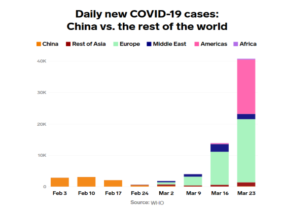
China’s fight against COVID-19 epidemic has achieved victory at this stage. Infected patients were found in 337 cities in China but now only 28 cities remaining patients in cure. So far till March 31st, there were 82545 confirmed cases in China, while 76225 cured and only 3006 remaining now. Most importantly, many of the areas finds only one figure number increase and others stop increasing for quite some days. If the first half of COVID-19 fighting is inside China national territory, the second half will be on the international stages while noticeable growth on COVID-19 infected cases are spreading all over the world now.
EBest Circuit (Best Technology) has been collecting the measures in China on epidemic controls so in order to provide a more objective and useful reference for overseas professionals which we hope they could refer to and protect better themselves from the COVID-19.
Governmental Measures
During the height of the outbreak, trains didn’t stop at the disease’s epicenter, Wuhan
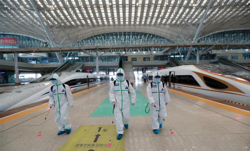
Trains, as well as other tightly packed forms of transportation, can serve as vectors of illness. The more people, the more closely packed, and the more poorly ventilated the space, you can imagine that’s a bad situation because there are a ton of people, they’re in very close quarters, and they’re a totally captive audience. Cutting off transportation was considered on the top three measures to contain the spread of the virus.
China built new hospitals in a rush, with workers toiling night and day to get them done.
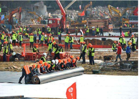
China built two new 1,000-1,300-bed hospitals to fight the corona virus, one created in six days, and the second in 15 days, using prefabricated modules.
Corona virus testing was easily accessible and free
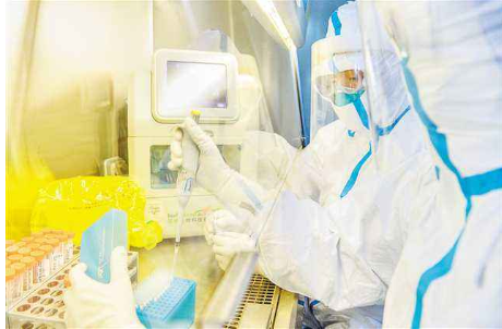
In China, patients who were confirmed to have the corona virus were either sent to an isolation center or hospital. The government also made clear that testing for the new virus was free, and COVID-19-related charges that weren’t covered by a person’s insurance would be paid for by the government.
The country implemented large-scale contact tracing in the early 2000s
During the SARS outbreak in 2002-2003, China set up large-scale surveillance systems that included contact tracing, a front-line public-health strategy that involves identifying and following up with people who may have come into contact with an infected person.
The country postponed non-urgent medical care and moved many doctor’s visits online. Not all patients were given the critical care they needed during the outbreak, though
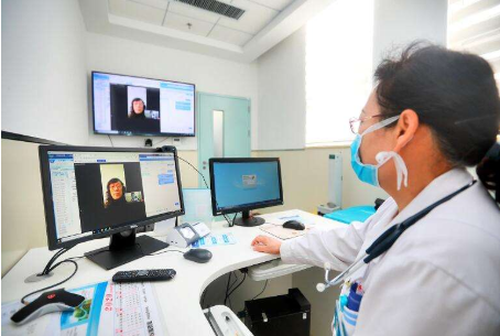
In China, elective surgeries and other non-critical doctors’ visits were delayed, and many medical services were moved online. Someone in one place said 50% of their consultations are now done online; they just moved a whole bunch of what was normally done physically online to be able to keep the regular health services going.
Centers for Disease Control exploring a way of therapeutic plan combing Traditional Chinese medicines and Western medicines.
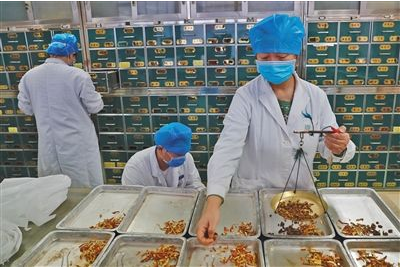
The combination of Traditional Chinese medicines and Western medicines had been proven effective on the SARS fights. Doctors of traditional Chinese medicines had volunteered for consulting and participating into the virus fights.
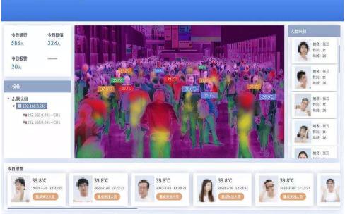
China used technology that aims to trace every single COVID-19 case
Civilian Measures
Traditional epidemic prevention manufacturers speed up and similar production lines integrating to make more necessary products

Many medicinal and pharmaceutical substances manufacturers launched automation assemble lines and increase manpower to speed up the mass production of necessary drugs, masks, ventilators to meet the huge consumption during virus fighting. Many of these companies arranged 24-hour shifts for maximizing the production.
Meanwhile other manufactures such as automotive OEM had change their assemble line into masks productions machines.
At the blast of COVID-19, returning Chinese carrying back epidemic products from overseas as much as they can
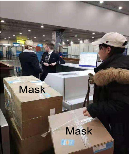
Returning travelers carried extra masks on their flights back to China and donated them to the hospital and governments in need. Some overseas Chinese unions also had helped ordering these products and sending to China.
Chinese citizens did their part to curb the disease’s trajectory on an individual level, too, though we may never know the true scale of their complaints or sacrifices in this outbreak.
In contrast to reports in the US of people clamoring over the last hand-sanitizer, the attitude of people in China was that they were all in this together. People stay at home for self-quarantine, lockdown and response to the postpone returning to work and school.
People who thought they might have the corona virus could go to one of the nation’s many fever clinics
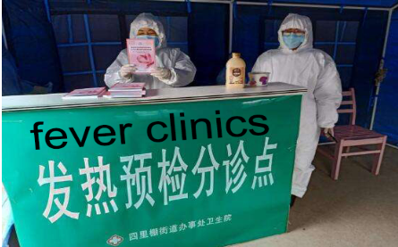
People who thought they had the novel corona virus in China would often be sent to a special fever clinic, which have been widespread since the country dealt with an aggressive SARS outbreak in 2002. Their temperature would be taken, and they’d discuss their symptoms, medical history, travel history, and any prior contact with anyone infected with a doctor.
If necessary, patients might receive a CT scan, which is one way to do an initial screening for COVID-19. Each machine did maybe 200 a day. 5-10 minutes/scan. A typical hospital in the West does one or two an hour.
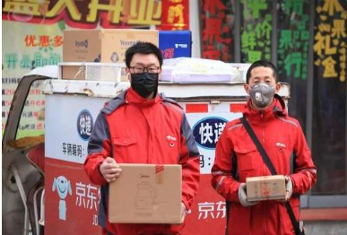
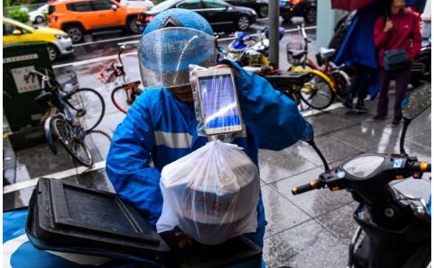
People quickly shifted jobs in order to assist during the outbreak
When it came to the non-medical response, there was a nationwide sense of solidarity with Hubei. Other provinces sent 40,000 medical workers to the center of the outbreak, many of whom were volunteers.
Workers in transportation, agriculture, and clerical positions were encouraged to new positions such as delivery, courier and epidemic prevention manufacturing, too.
While staying home, it’s been relatively easy for Chinese people to get extra food and supplies
China essentially mandated a country-wide shut down, demanding that every Chinese resident stay home until the curve was flattened. But in West, unlike China, a country-wide shutdown would be difficult to enforce.
Fifteen million people had to order food online. It was delivered. Yes, there were some screw-ups. But few said: every now and again there’s something missing from a package, but food supply is pretty much normal via ordering online.
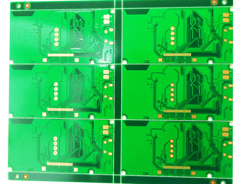
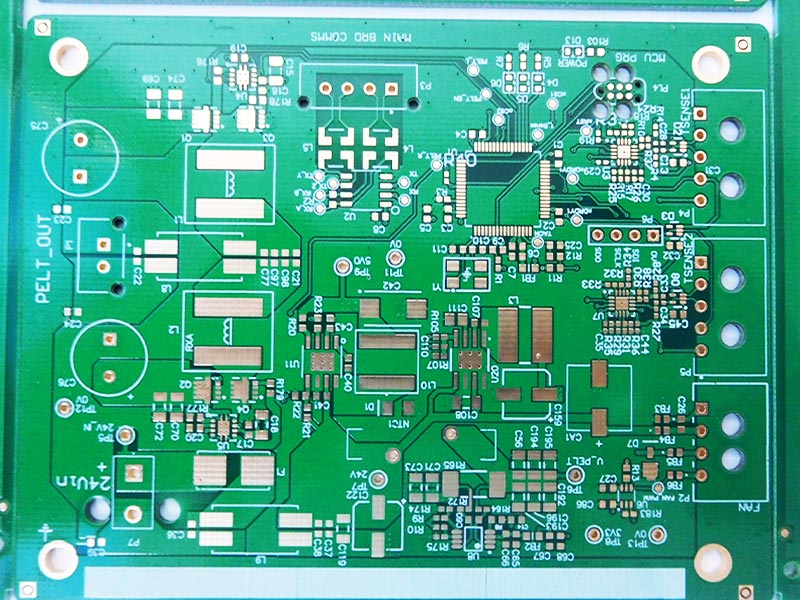
We know it’s difficult for most of people around the word to find protection devices, such as face mask, Non-surgical isolation gown , Medical gowns, protective coveralls, Surgical Cap, Surgical Dress , Medical gloves, Safety Goggles, Surgical Helmet, infrared thermometers, please contact our sales, we will be glad to support you.