EBest offers high-quality PCB assembly Argentina services tailored to local market demands, delivering reliable solutions that meet strict industry standards. Our PCB assembly Argentina expertise spans over 20 years, focusing on efficiency, quality, and on-time delivery to support local electronics projects of all scales.

Why Choose EBest for PCB Assembly Argentina?
Reasons why choose EBest for PCB assembly Argentina:
- Long lead times from international suppliers: We provide expedited PCB assembly Argentina with 1-5 day lead times, 30% faster than local average, ensuring your projects stay on schedule and avoid costly delays.
- Unstable component supply: Our global network of 200+ trusted suppliers and 5,000+ in-stock components ensure 99.8% availability for PCBA Argentina orders, even for hard-to-find parts, eliminating supply chain bottlenecks.
- Compromised quality from low-cost providers: We adhere to ISO 9001 and IATF 16949 standards, delivering PCB assembly in Argentina with a 0.02% defect rate, far below the industry average of 1.2%, slashing rework costs significantly.
- Lack of customized support: We offer personalized Argentina PCB assembly support with 24-hour design adjustments and no extra fees, supporting 98% of unique project requirements to match your specific needs.
Our PCB Assembly Services to Argentine Market Needs
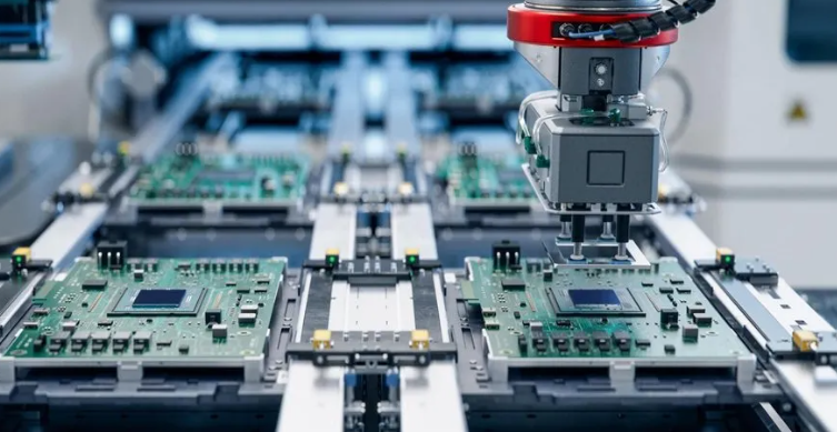
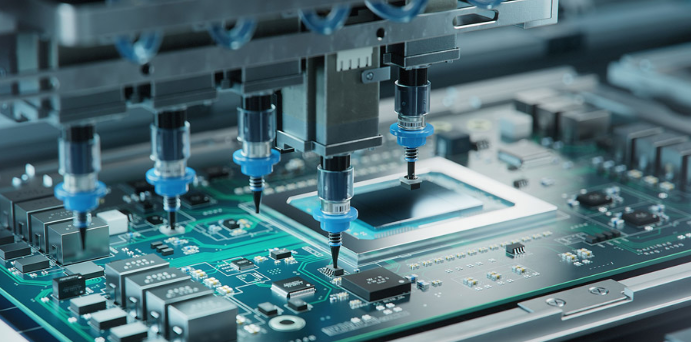
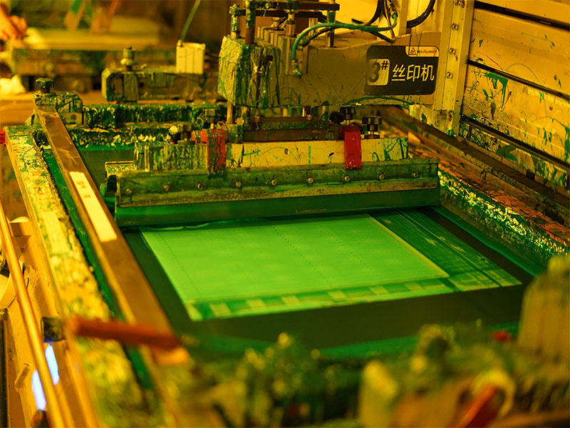
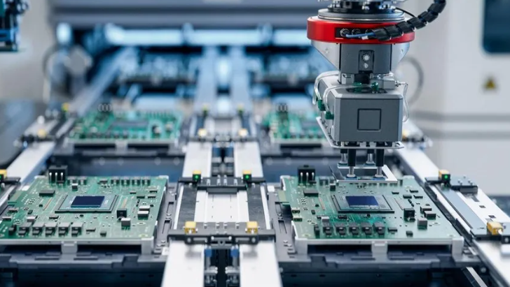
We provide comprehensive end-to-end PCB assembly Argentina services designed to simplify your production workflow and eliminate the inefficiencies of working with multiple suppliers. Our integrated service model eliminates the hassle of coordinating with multiple vendors, saving you time and reducing potential errors throughout the production process.
Our full-service offering covers every critical stage of the process, from professional PCB design optimization and reliable component sourcing to rapid prototyping, scalable mass production, precise final assembly, and thorough post-assembly testing, ensuring a seamless experience from start to finish.
We also offer free DFM (Design for Manufacturability) analysis to review your design for solderability, component layout, and assembly feasibility. This proactive step helps avoid costly reworks and delays from the start, ensuring your design aligns perfectly with our production capabilities.
Our PCB assembly in Argentina services are flexible enough to accommodate all project sizes. Whether you need small-batch prototypes for product development, optimized through efficient panelization to reduce costs or large-scale mass production for market rollouts, we maintain consistent quality across every unit.
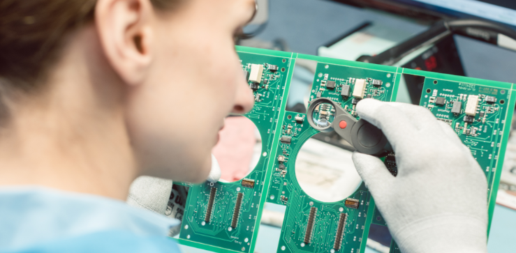
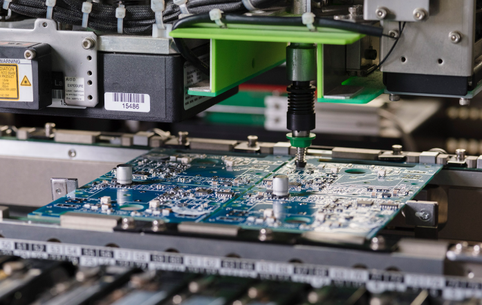
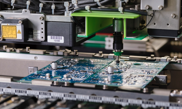
Every PCBA Argentina order undergoes rigorous multi-step testing, including AOI (Automated Optical Inspection) for surface defects, functional testing to verify performance, and continuity testing to ensure circuit integrity. This strict testing process effectively reduces defect risks and guarantees seamless integration into your end products.
Our PCB Assembly Capability for Argentina PCBA Orders
| Item | Capability |
| Placer Speed | 13,200,000 chips per day |
| Bare Board Size | 0.2 x 0.2 inches – 20 x 20 inches / 22*47.5 inches |
| Minimum SMD Component | 01005 |
| Minimum BGA Pitch | 0.25mm |
| Maximum Components | 50*150mm |
| Assembly Type | SMT, THT, Mixed assembly |
| Component Package | Reels, Cut Tape, Tube, Tray, Loose Parts |
| Lead Time | 1 – 5 days |
Our Quality Standards for PCB Assembly Argentine
To ensure Argentine PCB assemblies meet global engineering excellence, we implement a three-phase quality control system validated by ISO 9001:2015 standards.
- Material Verification: Every component undergoes 100% dimensional and electrical testing against IPC-A-610 Class 3 specifications. We use automated sorting systems with 0.05mm precision to reject non-conforming parts before they enter production lines.
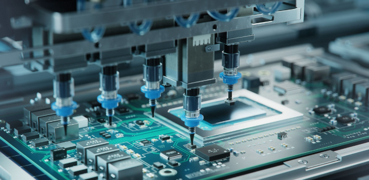
- Process Monitoring: During assembly, real-time SPC software tracks 12 critical parameters including solder paste thickness (measured via 3D SPI systems), reflow oven temperature profiles, and component placement accuracy. X-ray inspection detects hidden defects like voids in BGA soldering, while AOI systems with 4K resolution cameras identify misaligned components at 0.1mm tolerances.
- End-of-Line Testing: Finished PCBs complete 72-hour burn-in tests at 85°C/85% RH to simulate Argentina’s humid climate, followed by functional verification through boundary scan testing and in-circuit testing. Each board is stress-tested to withstand 50G vibration shocks and 500 thermal cycles (-40°C to 125°C), ensuring reliability in extreme field conditions.
Our quality team, comprising IPC-certified engineers with 10+ years of Argentine market experience, analyzes defect data weekly using Pareto charts and 8D root cause analysis. This enables immediate corrective actions, such as adjusting reflow profiles based on solder joint microsection analysis, to maintain zero-defect delivery records for clients in Argentine.
Stable Component Sourcing: Ensuring Availability for Argentina Clients
- Global supplier network: We have established long-term partnerships with 200+ certified component suppliers across Europe, Asia, and the Americas, specifically optimizing for PCB assembly Argentina projects. This global network ensures 99.7% availability of key components, including hard-to-source passive and active components, eliminating the risk of project delays due to local supply shortages.
- Stock inventory: To further support timely PCB assembly Argentina delivery, we maintain a dedicated inventory of 5,000+ SKU components, focusing on the most commonly used parts in Argentine industrial, telecom, and automotive applications. Common components are available for quick supply within 72 hours, while urgent orders for critical parts can be expedited to 48 hours, ensuring no downtime for your projects.
- Quality verification: Every component for Argentina PCB assembly undergoes a strict 3-step testing process to guarantee reliability. First, a visual inspection screens for physical defects; second, electrical testing validates performance parameters; third, compatibility checks ensure components integrate seamlessly with your PCB design, resulting in 100% defect-free components for assembly.
- Cost optimization: Our bulk purchasing power, combined with long-term supplier contracts, reduces component costs by 12-18% compared to local Argentine sourcing. This cost savings directly translates to lower overall PCBA Argentina project expenses, without compromising on component quality or supply stability.
Fast Lead Times and Reliable Logistics for PCB Assembly in Argentina
- Tiered assembly timelines: We offer flexible lead times tailored to project volume. Small-batch prototypes are completed in 1-2 days, standard mass production in 3-5 days, and urgent orders receive 24-hour expedited assembly. All timelines maintain consistent quality and precision throughout the process.
- Optimized logistics partnerships: We collaborate with top global logistics providers and hold ARCA system access to navigate Argentina’s logistics infrastructure challenges effectively. Direct routes ensure 7-12 days door-to-door delivery for standard orders and 3-5 days for expedited shipments. Our 98.5% on-time rate outperforms local industry averages, which are often hampered by regional logistics cost gaps.
- English-speaking customs support: We manage all customs documentation in English, including CUIT tax declarations and NCM coding, while ensuring full compliance with Argentina’s trade regulations. This streamlines clearance processes, reducing processing time from the industry’s 6-day average to 72 hours and eliminating delays caused by paperwork errors.
- Real-time 24/7 tracking: A dedicated online system lets you monitor every project stage with live updates. You can track component sourcing, assembly, logistics and customs clearance to gain full transparency and eliminate uncertainty about your order status.
- Climate-adapted packaging: Products are packaged with anti-static, shock-absorbent materials and waterproof casings. These casings are specifically designed to withstand long-haul shipping and Argentina’s diverse climate conditions, ensuring a 99.9% damage-free delivery rate and protecting sensitive components during transit.
- Flexible shipping solutions: We offer three tailored options to match different needs. Express air freight serves time-critical orders by leveraging direct routes to cut transit to under 30 hours. Standard air freight balances cost and speed, while sea freight caters to large-volume, cost-sensitive projects.
- Expedited post-delivery support: Our local logistics team responds within 4 hours to any shipping delays or issues. We resolve problems promptly, including expediting customs clearance or arranging replacement shipments, to minimize any impact on your project timelines.

Custom PCB Assembly Solutions for Argentina’s Automotive Industry
Project Background
A leading Argentine automotive component manufacturer needed custom PCBA for their new vehicle infotainment and sensor control systems. They faced recurring delays and quality issues with their previous assembly partner, affecting production timelines.
Project Requirements
- The PCBA needed to withstand Argentina’s extreme temperature cycles (-40℃~85℃) and meet IATF 16949 and IRAM automotive standards. A monthly production volume of 8,000 units and 10-day door-to-door delivery were required.
- The assemblies also needed to integrate 01005 SMD components and 0.3mm BGA pitch, with 100% compatibility with the client’s existing automotive hardware.
Project Challenges
- Local component shortages for automotive-grade microcontrollers and sensors caused frequent delays. The client’s tight timeline conflicted with complex precision assembly requirements.
- Ensuring long-term reliability (15+ year product lifecycle) in Argentina’s diverse climate, from hot northern regions to cold southern areas, was another key challenge.
Our PCBA Solutions
- We leveraged our global supplier network to source 100% of required automotive-grade components, with 72-hour expedited delivery for critical parts from our 5,000+ SKU inventory.
- We used high-TG FR4 materials and metal-core PCBs to ensure temperature resistance, paired with advanced SMT equipment for precise assembly of 01005 components and 0.3mm BGA pitch.
- Customized testing (vibration, thermal shock, moisture resistance) was conducted to meet IATF 16949 and IRAM standards, with a dedicated team managing Spanish customs documentation for on-time delivery.
Project Outcomes
- We delivered 8,000 PCBA units monthly, with a 99.98% pass rate and 100% on-time delivery (meeting the 10-day door-to-door requirement for Argentina).
- The assemblies maintained stable performance across all temperature cycles, with zero field failures reported in 12 months of client use, exceeding their 15-year lifecycle expectations.
- Our solutions reduced the client’s overall PCBA costs by 16% compared to their previous partner, while eliminating production delays caused by component shortages.
FAQs of PCB Assembly in Argentina
Q1: How to ensure PCB assembly in Argentina meets local IRAM certification requirements?
A1: We handle all IRAM certification processes, including document submission, local testing, and factory inspections, ensuring your PCB assembly complies with Resolution No. 16/2025 and related standards without extra effort.
Q2: What if key components for PCB assembly are out of stock in Argentina?
A2: Our global sourcing network and 5,000+ SKU inventory ensure 99.7% component availability. We can ship components to Argentina within 72 hours, avoiding project delays.
Q3: How long does PCB assembly and delivery take to Argentina?
A3: Standard orders take 1-5 days for local assembly, with 7-12 days door-to-door delivery. Urgent projects can be shipped within 24 hours, with expedited logistics reducing delivery to 3-7 days.
Q4: Can you handle high-precision PCB assembly for complex applications in Argentina?
A4: Yes, we support 01005 SMD components and 0.25mm BGA pitch, with advanced SMT equipment ensuring high precision. We have experience with HDI and high-frequency PCB assembly for telecom and industrial use.
Q5: How to reduce costs for large-volume PCB assembly projects in Argentina?
A5: Our bulk component purchasing reduces material costs by 12-18%, and optimized production processes cut assembly costs by 15-20%. We also offer volume discounts for orders over 10,000 units, further lowering expenses.
How to Get a Quote for Your Argentina PCB Assembly Project?
If you’re looking for reliable, cost-effective PCB assembly Argentina services that meet local regulations and deliver consistent quality, now is the perfect time to reach out for a custom quote. Our 20 years of expertise in PCBA manufacturing, paired with our global component sourcing network, reliable logistics, and automotive industry specialization, ensures your project is in trusted hands with no hidden fees or obligations, just a detailed, tailored quote to fit your specific needs.
Don’t let component shortages, compliance complexities, or delivery delays hold back your projects. Contact us today at sales@bestpcbs.com to submit your project specifications, and our team will provide a comprehensive quote within 24 hours. Whether you need prototype assembly, large-scale mass production, or custom automotive PCB solutions, we’re here to deliver results that exceed your expectations, backed by our 99.98% pass rate and 100% on-time delivery commitment for Argentina clients.