In our daily life, electronic devices are existing everywhere. And there are many people know the “PCB” nowadays, while very less people know the “PWB”. Unless you’ve been in the PCB business for more than 20 years.
Actually, PWB is another term of circuit board, and it was used commonly before the year 1999. But with the development of electronics, it was replaced by PCB gradually. You want to know more about it? In this article, we will answer it for you. Deeply explain their definitions, manufacturing process, applications and the key differences between PCB and PWB.
What is A Printed Circuit Board (PCB)?
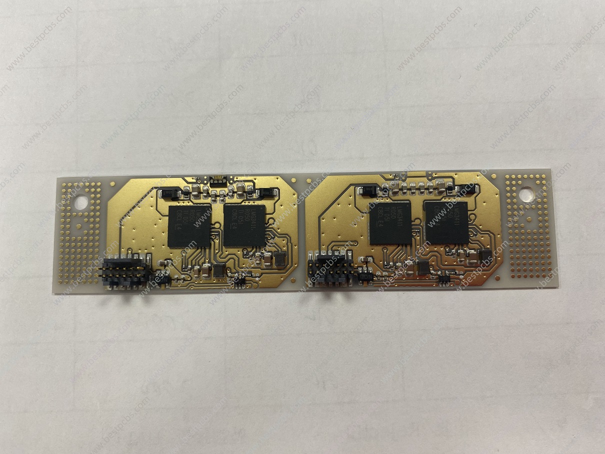
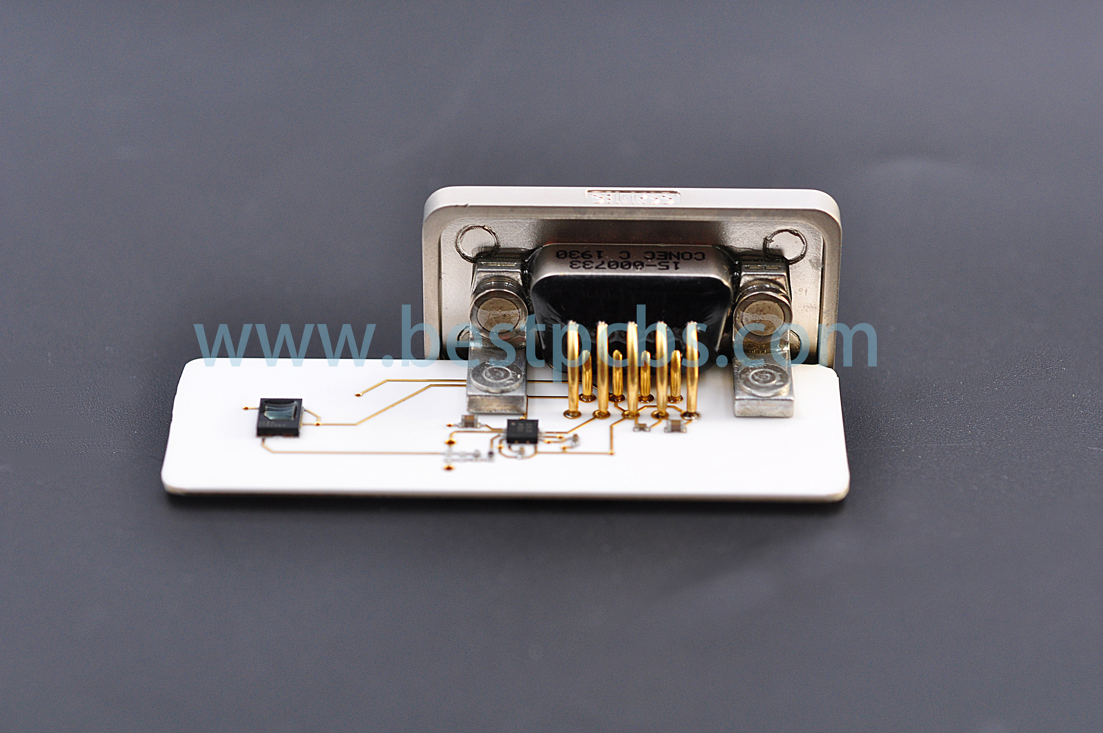
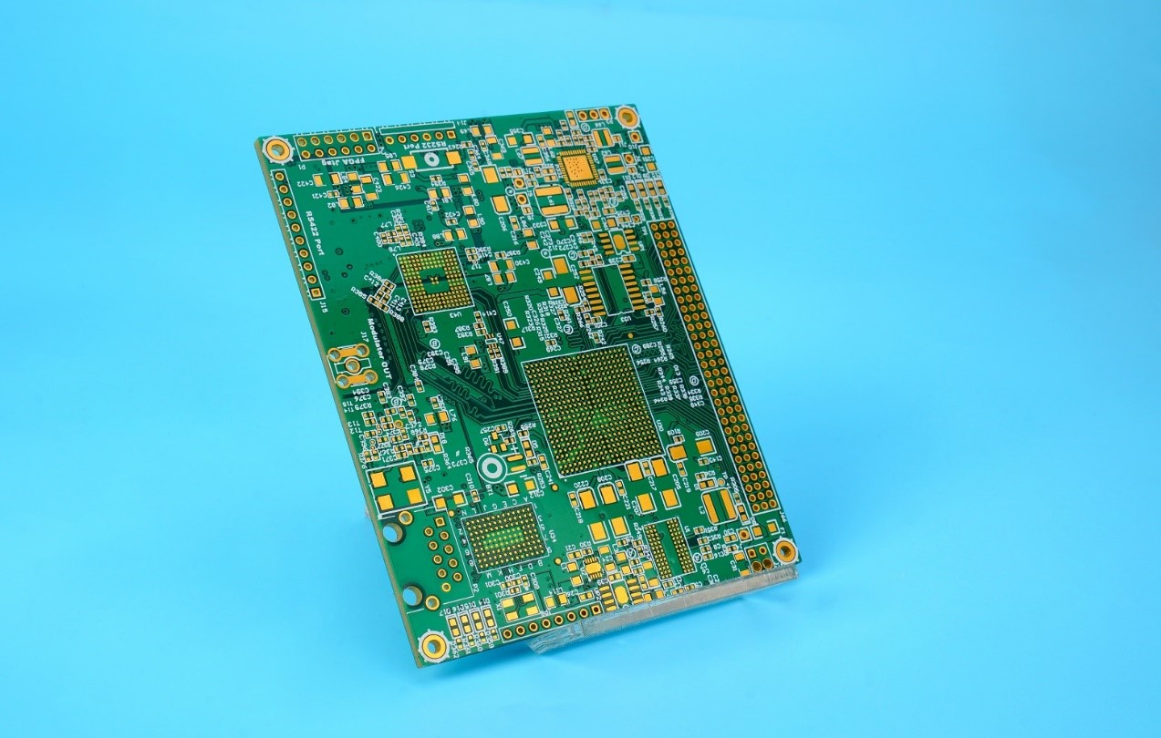
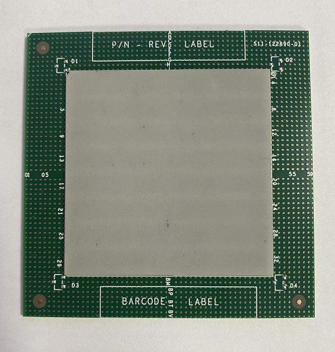
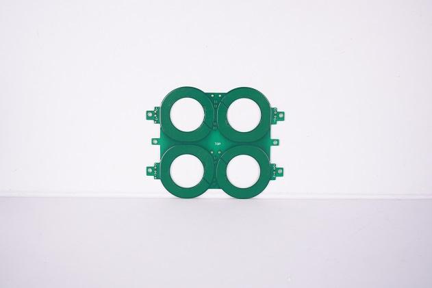
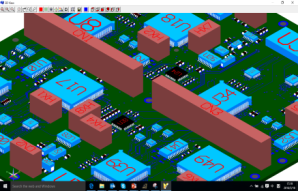
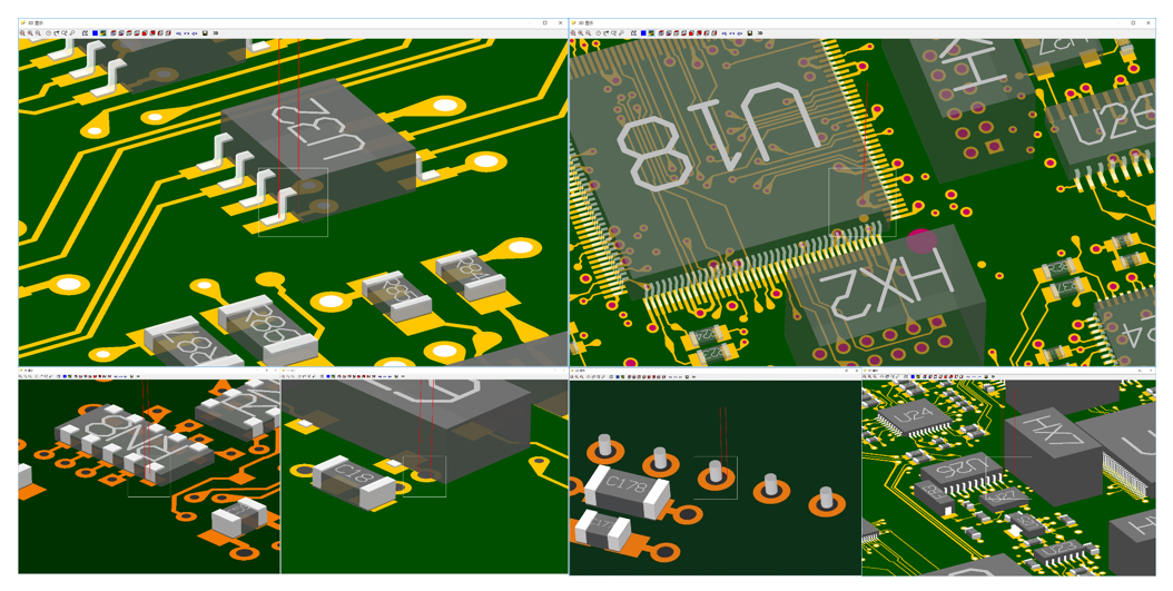
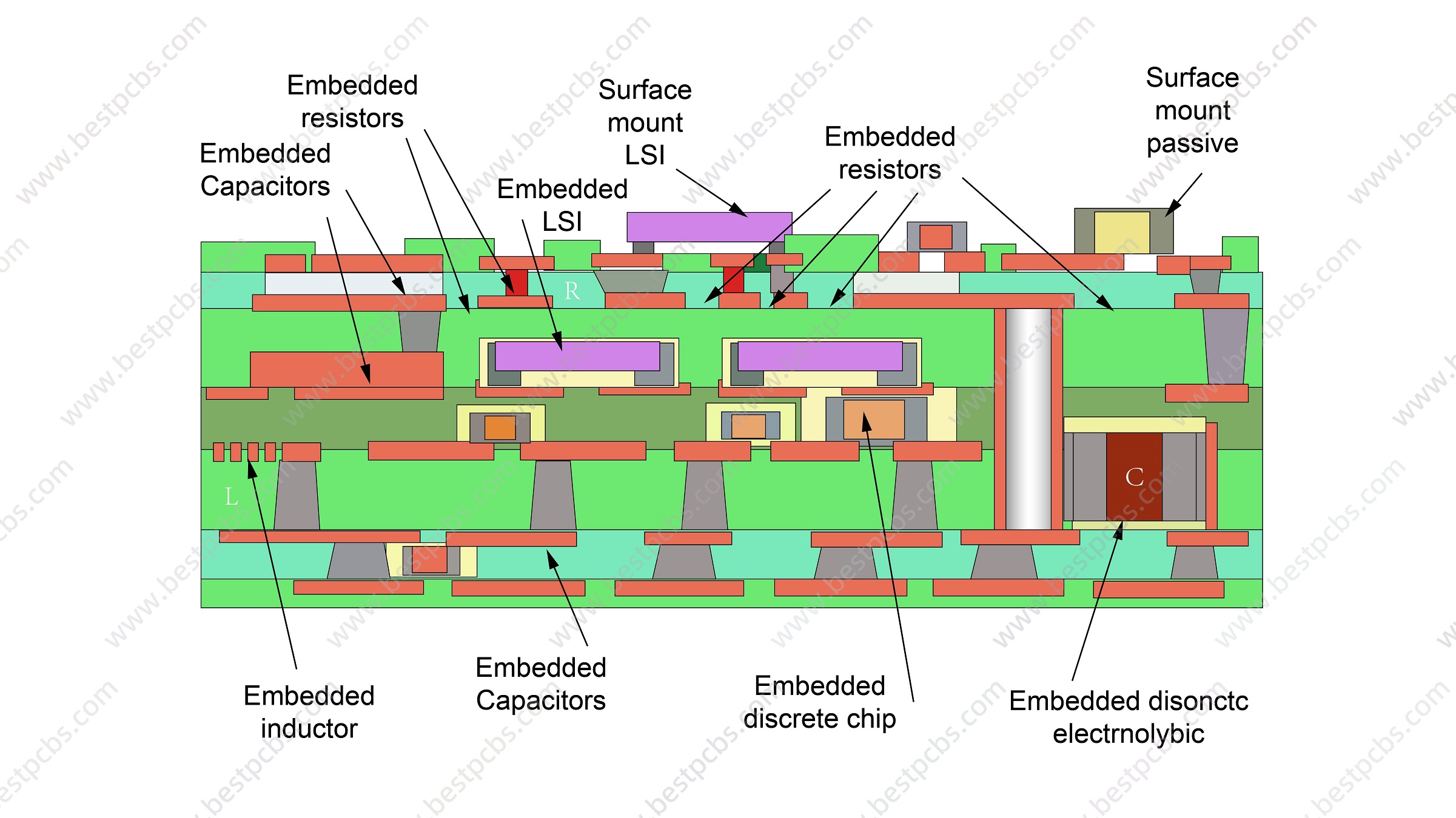
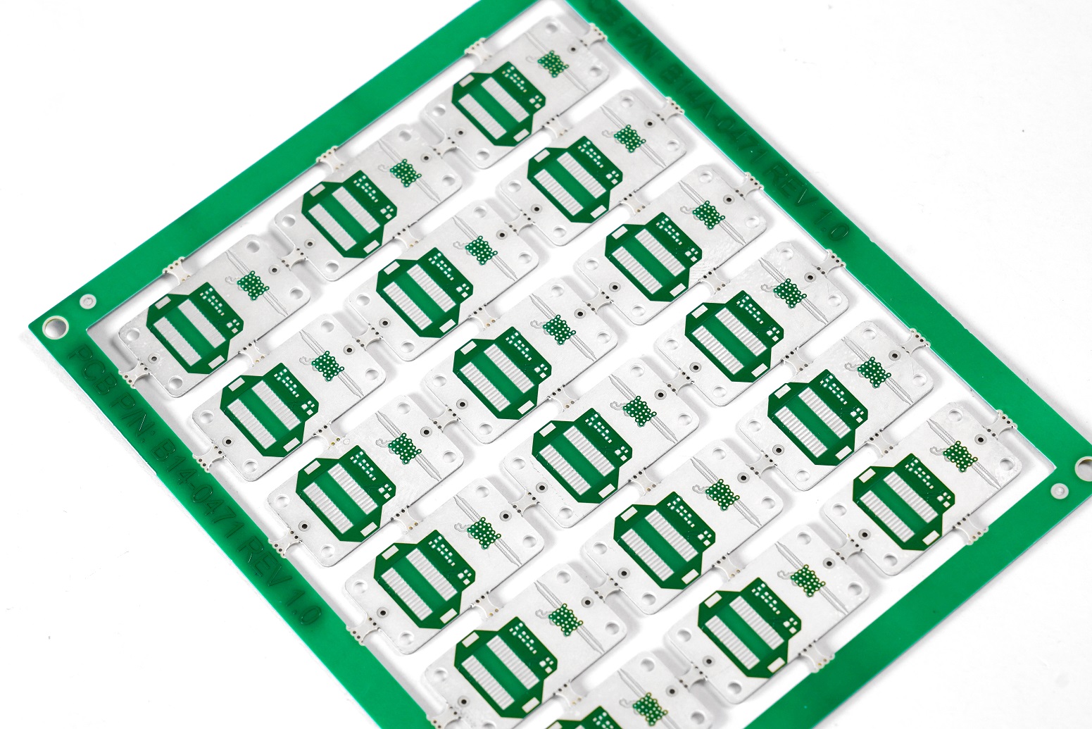
A Printed Circuit Board is a fundamental component in modern electronics, providing the physical and electrical connections for various electronic components. It consists of multiple compositions, including a non-conductive substrate, conductive pathways, and insulating layers, which facilitate the complex circuitry required in contemporary devices. A PCB can be made into single sided PCB, double sided PCB and multilayer PCB.
PCBs are integral to the functionality of a wide range of electronic products, from consumer gadgets like smartphones and computers to industrial machinery, medical devices, and aerospace systems. The advanced design and manufacturing processes involved in PCB production ensure high reliability and performance, making them essential in virtually all electronic applications.
Basic manufacturing process of PCB
Design and Layout
PCBs are designed using sophisticated computer-aided design (CAD) software. Designers create detailed layouts, specifying the placement of components, conductive pathways, and vias (interlayer connections). The design is converted into Gerber files, a standard format for PCB fabrication that contains all the necessary information for manufacturing. These files are essential for ensuring precision and accuracy during the manufacturing process.
Material Preparation
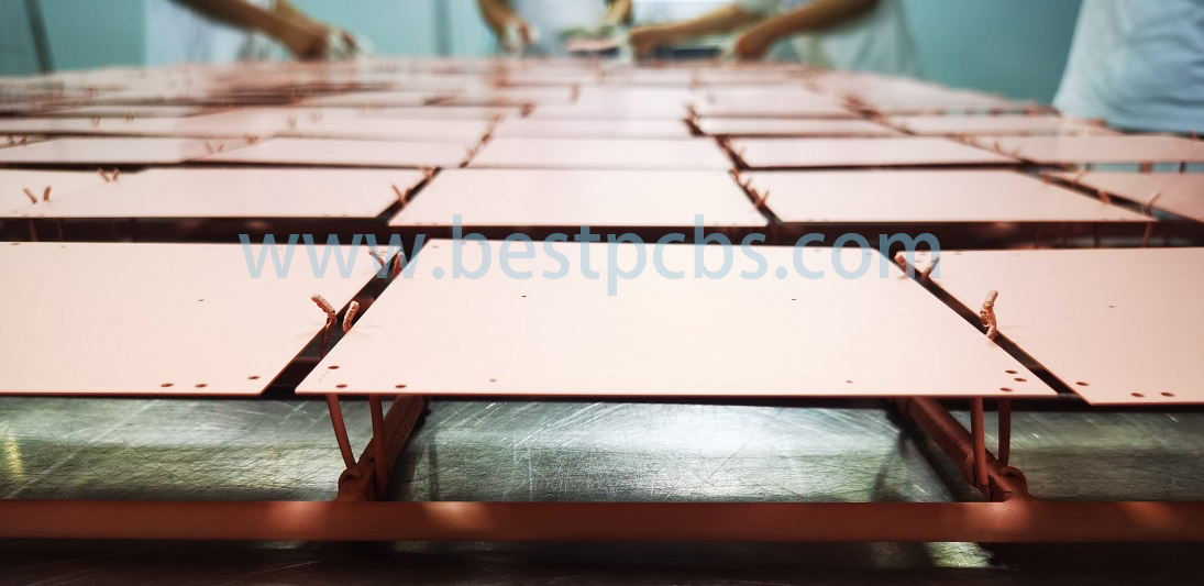
The substrate, typically FR4 (fiberglass epoxy laminate), is prepared. FR4 is known for its excellent mechanical strength and thermal stability, making it an ideal base material for PCBs. Copper sheets are laminated onto the substrate, which will form the conductive pathways after the etching process. This preparation stage is crucial for creating a reliable foundation for the PCB.
Printing the Circuit Pattern
A photoresist, a light-sensitive material, is applied to the copper-clad substrate. The board is exposed to ultraviolet (UV) light through a mask that defines the circuit pattern. The UV light hardens the photoresist in the exposed areas. The board is then developed in a chemical solution that removes the unexposed photoresist, revealing the copper to be etched away. This step accurately transfers the circuit design onto the board.
Etching
The board is immersed in an etching solution, commonly ferric chloride or ammonium persulfate, which removes the unprotected copper, leaving only the desired circuit pattern. This etching process is crucial for defining the conductive pathways on the PCB, ensuring that the correct connections are made according to the design specifications.
Drilling
Precision drilling machines are used to create holes for through-hole components and vias. These holes are then cleaned to remove any debris that could affect electrical connectivity. Drilling is a critical step in the PCB manufacturing process as it ensures proper placement and connection of components across different layers of the board.
Plating
The drilled holes are plated with copper to create electrical connections between the layers, which is especially important for multilayer PCBs. Additional layers of plating, such as nickel or gold, may be applied to improve conductivity and protect against oxidation. This plating process enhances the durability and performance of the PCB.
Solder Mask Applying
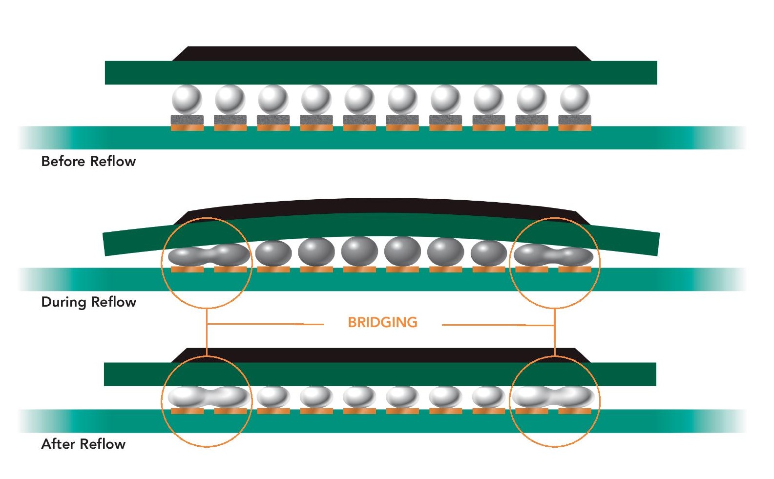
A solder mask is applied to protect the copper traces from oxidation and prevent solder bridges between closely spaced solder pads. The solder mask is exposed to UV light and then developed to reveal the solder pads. This layer not only protects the PCB but also improves its appearance and reliability.
Silkscreen Printing
A silkscreen layer is printed on the board to add text, component labels, and other identifiers. This layer helps in the identification and assembly of components, making it easier for technicians to work with the PCB during the manufacturing and repair processes.
Surface Finishing
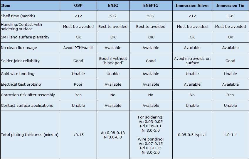
Generally, a layer of surface finishing is coated on the PCB to protect its surface, it also called surface treatment. The common surface treatments are HASL-LF, ENIG, ENEPIG, OSP, Immersion Silver/Tin. Of course, different treatment offers different function, like OSP is to protect surface from oxidation, HASL-LF provides a good solderability, ENEPIG make sure the chemistry corrosion. Choose a suitable one according to your specific demands.
Assembly and Testing
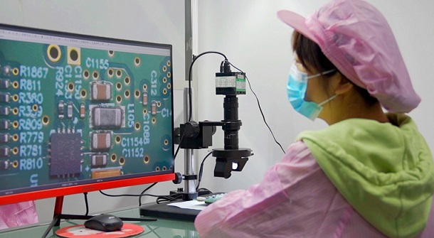
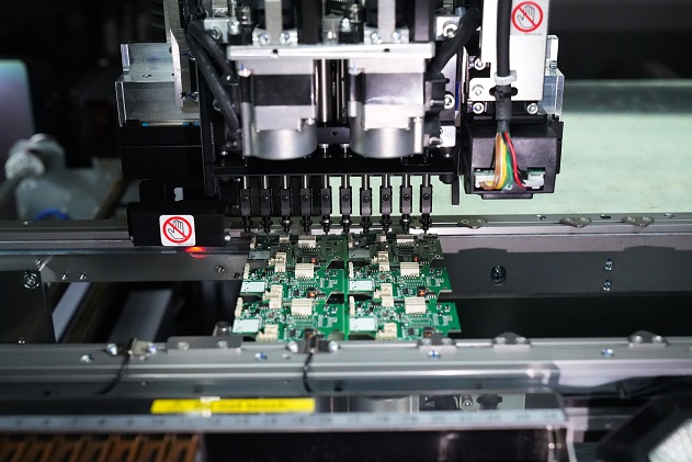
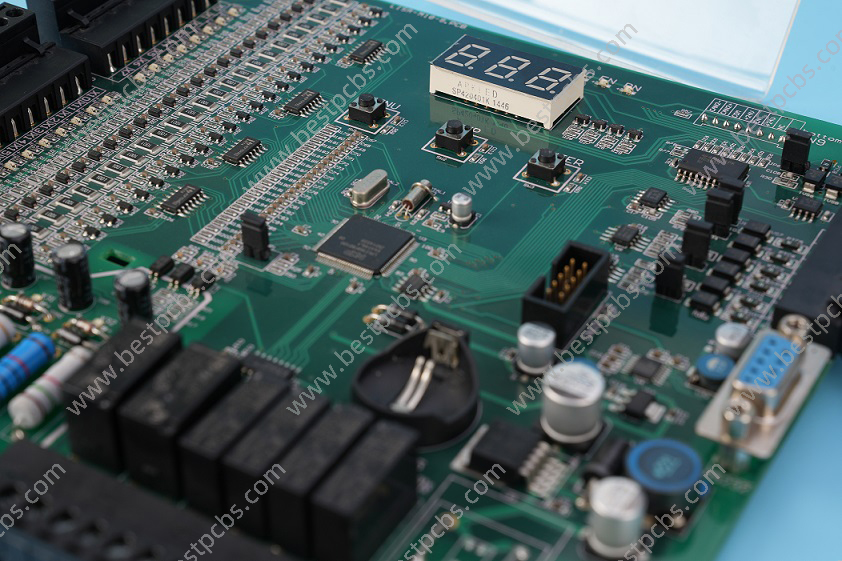
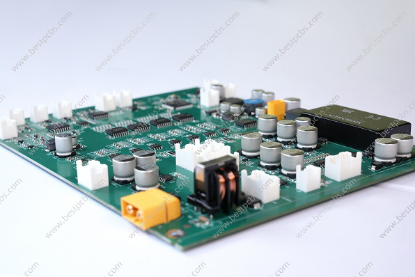
Components are placed on the board using automated pick-and-place machines, and soldered using techniques like reflow soldering for surface-mount devices (SMD) and wave soldering for through-hole components. The finished PCB undergoes various tests, such as automated optical inspection (AOI), electrical testing, and functional testing, to ensure quality and performance. Want see the whole manufacturing process of a multilayer PCB, click here: Manufacturing Process of Multi-layer PCB.
What is the definition of Printed Wiring Board (PWB)?
A Printed Wiring Board is a term historically used to describe a type of circuit board that focuses primarily on the layout and wiring of electronic connections rather than the overall circuit functionality. PWBs emphasize the physical arrangement of conductive paths to connect various components but do not necessarily include all the integrated features found in modern PCBs.
This term was more prevalent during the earlier stages of electronic development, where the primary concern was establishing reliable electrical connections. As technology advanced, the term PCB became more common, reflecting the expanded capabilities and comprehensive role of these boards in forming complete electronic circuits. Despite being less common today, understanding the term PWB is crucial for historical context and certain niche applications.
How to Manufacture A Printed Wiring Board (PWB)?
Design and Layout
PWBs typically have simpler designs focused on wiring patterns rather than complex circuitry. In some cases, the layout may be done manually or using basic design software.
Material Preparation
Simpler substrates such as phenolic or epoxy resins may be used for PWBs. Copper sheets are laminated onto the substrate to form the conductive pathways. These materials are cost-effective and suitable for applications where advanced performance characteristics are not required.
Printing the Wiring Pattern
Similar to PCBs, a photoresist is applied to the copper-clad substrate. The board is then exposed to UV light through a mask and developed to reveal the copper to be etched away. This process creates the wiring pattern necessary for connecting electronic components.
Etching
The board is immersed in an etching solution to create the wiring pattern. This step is straightforward compared to the more intricate etching processes used in PCB manufacturing, reflecting the simpler requirements of PWBs.
Drilling
Holes for through-hole components are drilled, but the process may not require the precision needed for complex PCBs. This basic drilling process is adequate for the less demanding applications of PWBs.
Plating (if necessary)
Plating is done to ensure electrical connectivity but may not involve advanced techniques like those used for multilayer PCBs. It suffices for the simpler construction of PWBs.
Solder Mask Application
A basic solder mask may be applied to protect the wiring pattern. This layer provides sufficient protection for the relatively simple designs of PWBs, preventing short circuits and oxidation.
Silkscreen Printing
A simple silkscreen layer may be added for component identification. This helps in the assembly process but does not require the detailed labeling often necessary for PCBs.
Assembly and Testing
Components are manually or semi-automatically placed on PWBs and soldered using standard techniques. Basic electrical testing is conducted to ensure functionality. This simpler assembly and testing process aligns with the less complex nature of PWBs.
Which Kind of Materials used in PCB and PWB?
Substrate Materials
FR4 (fiberglass epoxy laminate) is the most common substrate material for PCBs due to its excellent mechanical strength and thermal stability. Phenolic resin, used in PWBs for simpler applications, is less durable and has lower thermal stability compared to FR4, but it is cost-effective and suitable for basic electronic devices. Polyimide is used for flexible PCBs due to its high flexibility and thermal resistance, making it ideal for applications requiring bending and flexing, such as wearable electronics and flexible displays.
Conductive Materials
Copper is the primary conductive material for both PCBs and PWBs. It is used to create the conductive pathways and pads, providing excellent electrical conductivity and reliability. Gold, nickel, and silver are used for plating to enhance conductivity and protect against oxidation, primarily in PCBs. These materials improve the durability and performance of the PCB by providing a reliable contact surface for soldering and component connections.
Insulating Materials
Prepreg, a fiberglass cloth impregnated with resin, is used in multilayer PCBs to bond the layers together. Prepreg provides mechanical strength and electrical insulation between the layers. Dielectric materials are used between layers in multilayer PCBs to provide electrical insulation, maintaining signal integrity and preventing short circuits.
Solder Mask Materials
Liquid Photo Imageable (LPI) solder mask is the most common type used in PCBs, providing excellent protection and durability. LPI solder masks are applied using a photolithographic process, ensuring precise coverage and protection. Dry film solder mask is used for simpler applications and PWBs. This type of solder mask is less expensive and easier to apply but may not offer the same level of protection as LPI solder masks.
Key differences between PCB and PWB
| Feature | PCB (Printed Circuit Board) | PWB (Printed Wiring Board) |
| Design and Layout | Designed using sophisticated CAD tools for complex circuitry, including detailed simulation and optimization. | Simpler designs focused on wiring patterns, often done manually or with basic software. |
| Layer Count | Can have multiple layers (e.g., double-sided, multilayer) to support intricate circuit designs. | Generally single or double-sided, less commonly multilayer. |
| Component Types | Supports surface-mount technology (SMT) and through-hole technology (THT) components. | Primarily supports through-hole technology (THT) components. |
| Signal Integrity | Designed to maintain high signal integrity, minimizing electrical noise and interference. | Basic signal integrity management, sufficient for simple applications. |
| Flexibility and Rigidity | Includes both rigid and flexible PCBs, allowing for a wide range of applications. | Typically rigid, not commonly used in flexible applications. |
| Terminology and Usage | Universally used in the industry to refer to boards that integrate all necessary components to form complete circuits. Also called “bare board”. | Universally used in the industry to refer to boards that integrate all necessary components to form complete circuits. |
| Industry Standards | Recognized by standards organizations like IPC, IEC, and ANSI with specific performance and quality criteria. | Covered under broader standards but with fewer specific guidelines due to limited modern use. |
| Cost and Efficiency | Higher cost due to advanced materials and processes, offering superior performance and reliability. | More cost-effective for simple applications, but with limited performance and reliability. |
| Applications | Used in consumer electronics, industrial equipment, medical devices, aerospace, and defense. | Historically used in simpler electronic devices and early computers, still relevant in niche applications. |
Other Terms Related to PWB and PCB
Based on the PCB and PWB, you may still hear about CCA, PCA, PWA during the PCB working. These terms are also related to printed circuit board. Here is a detailed explanation of each:
Printed Wiring Assembly (PWA)
PWA is the abbreviation for printed wiring assembly. This is an archaic term that was once used to describe what we now refer to as PCB assembly or PCBA. Although it is less common today, understanding this term is useful for historical context and when dealing with older documentation.
Circuit Card Assembly (CCA)
CCA stands for circuit card assembly. It is essentially the same thing as PCBA, where the PCB is assembled with all necessary components to create a functional unit. CCA is a less frequently used term compared to PCBA but is still recognized in certain industries and contexts.
Printed Circuit Board Assembly (PCBA)
PCBA is the abbreviation for printed circuit board assembly. When the PCB is assembled with all its electronic components by SMT technology, it is called PCBA or PCB assembly. Since a change in terminology in 1999, PCBA has become the standard term used for all assembled circuit boards. From users to technical committees, PCBA is the preferred term for referring to assembled boards. The assembly process involves placing and soldering components onto the PCB, making it a functional electronic circuit.
Printed Circuit Assembly (PCA)
PCA stands for printed circuit assembly, which is another term for PCBA. Like CCA, PCA is not commonly used in modern terminology but refers to the same concept of an assembled printed circuit board.
In a word, whatever for PWB, PCB, or circuit cards, they are refer to bare printed circuit boards (bare boards). While PCA, CCA, PWA, and PCBA refer to assembled circuit boards. Among these terms, PCB and PCBA are the most widely used in both industry and technical documentation.
This is the end of this introduction of PWB and PCB, welcome to contact us if you want more about PCB knowledge.


.jpg)