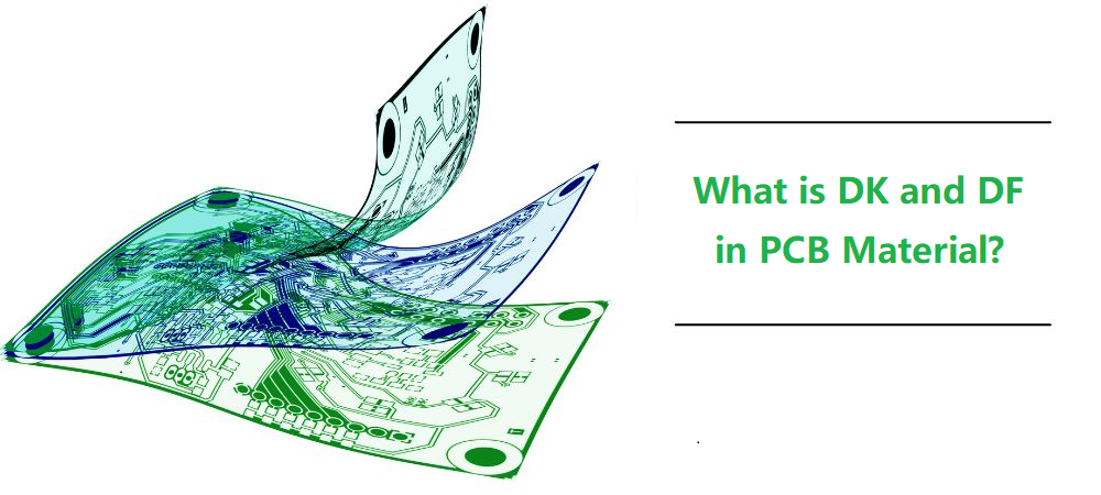
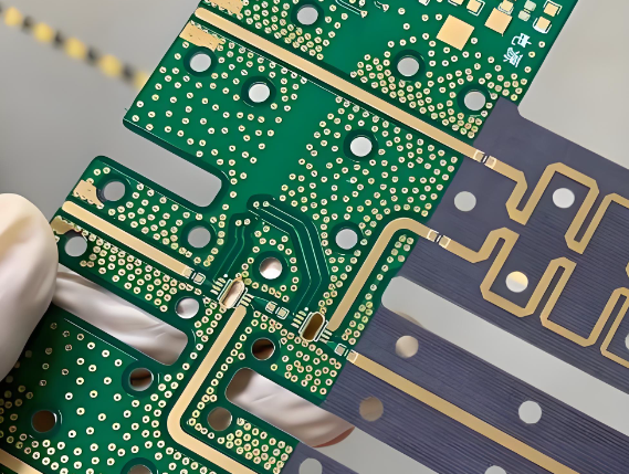
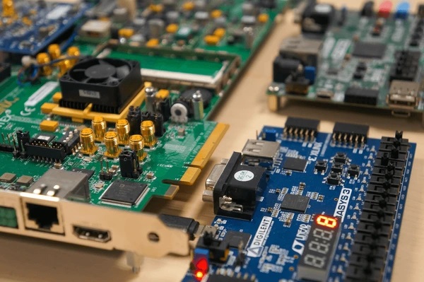
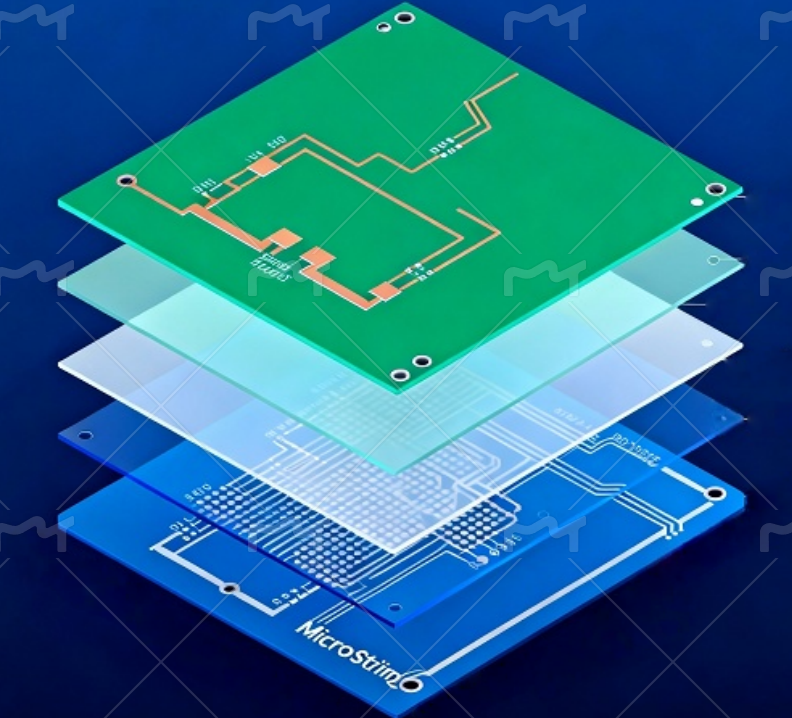
In any RF PCB material used for wireless modules, radar systems, or 5G designs, few parameters influence performance as strongly as DK, or dielectric constant. When engineers talk about controlled impedance PCB structures, DK sits at the heart of every decision. It shapes signal speed, impedance behavior, and even how your RF transmission line behaves at microwave frequencies.
If your goal is stable, predictable high-frequency PCB design, understanding why DK matters will help you choose better laminates and avoid costly tuning steps.
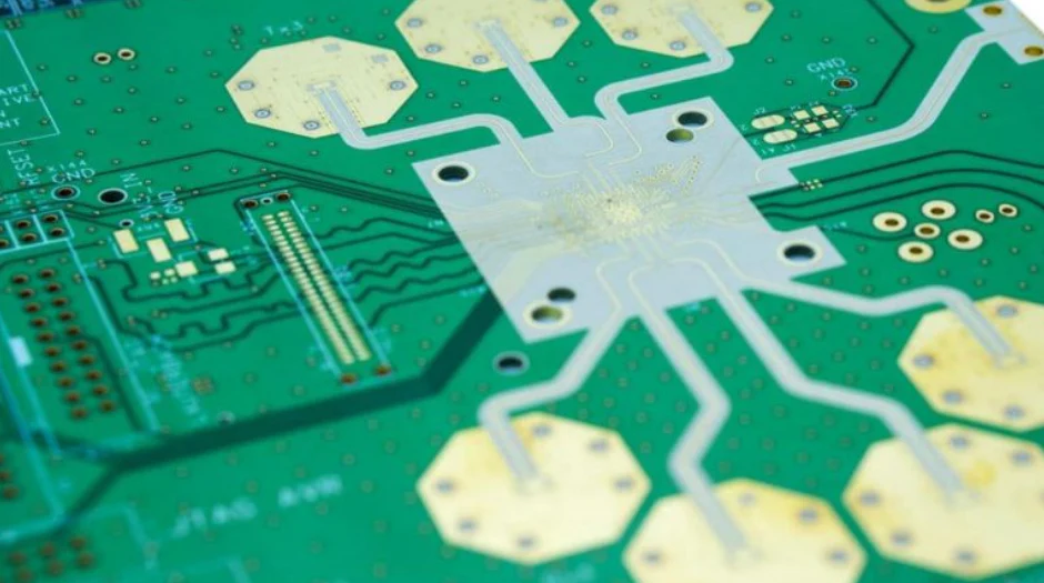
DK Directly Determines the Impedance of RF Transmission Lines
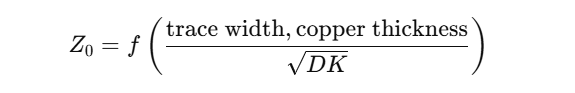
Every RF microstrip impedance calculation depends on DK. The material’s dielectric constant feeds into the formula that sets the final impedance for 50Ω microstrip lines, 75Ω video lines, and many custom RF structures.
The relationship is simple:
- Higher DK → lower impedance
- Lower DK → higher impedance
This is why RF PCB stack-up design can only be accurate when the underlying DK is consistent. Even a small DK shift, such as ±0.1, can move the impedance by several ohms. At microwave frequencies, that difference influences return loss, matching accuracy, and the stability of filters or antennas.
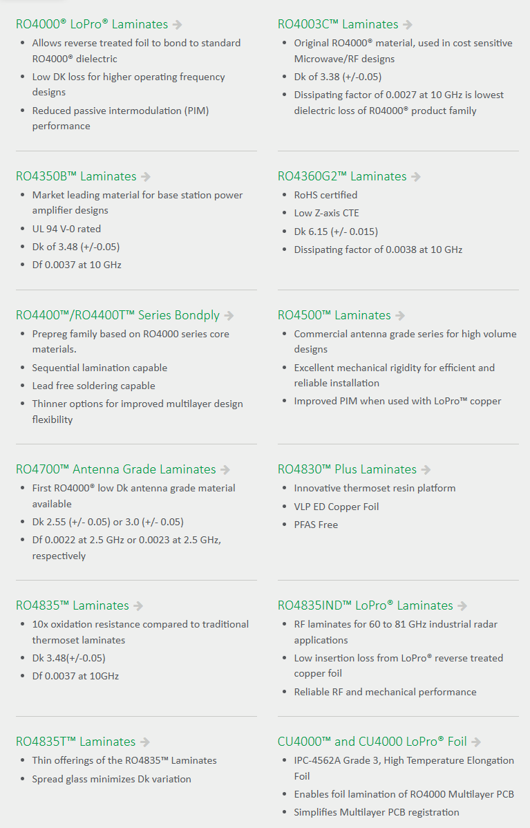
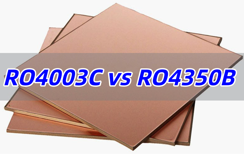
To reduce this variation, engineers often choose Rogers RF materials such as RO3003, RO4003C, and RO4350B, which maintain tighter DK tolerance than conventional FR4.
DK Stability Protects RF Circuits From Impedance Drift
Standard materials, such as FR4, show large DK swings at different frequencies and temperatures. But advanced high-frequency laminate materials are engineered for stability across environmental changes, humidity, and frequency ranges.
Stable DK provides stable impedance, which leads to:
- cleaner signal flow
- predictable matching in RF front-end circuits
- stable phase length for microwave structures
- consistent RF PCB routing performance
For microwave builds, especially above 2–3 GHz, DK tolerance becomes one of the clearest indicators of high-quality RF PCB material selection.
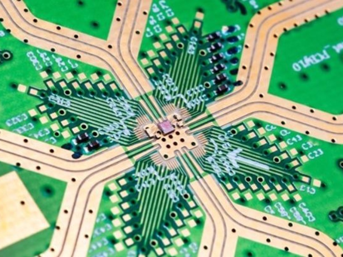
DK Controls RF Signal Propagation
Impedance is not just a number—it reflects how electromagnetic energy moves across the PCB. DK defines the relationship between the electric field in the trace and the dielectric beneath it. When DK is stable, signal propagation speed stays stable too.
This affects many RF structures:
- microstrip antennas
- transmission lines for mixers, LNAs, and PAs
- VCOs and PLL circuits
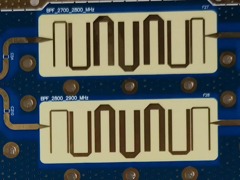
- bandpass filters and couplers
- phased-array elements
- radar transceiver lines
With stable DK, these structures behave closer to their modeled performance, reducing the risk of frequency drift or unexpected resonance shifts.
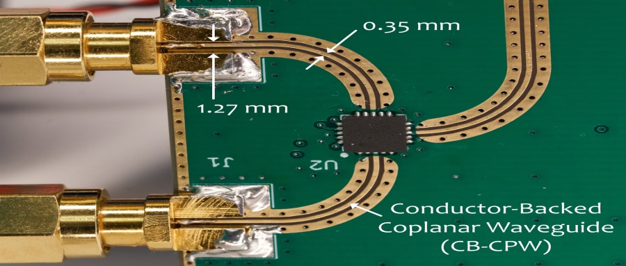
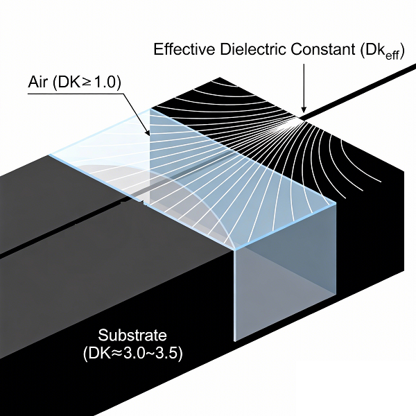
DK Influences Effective Permittivity (Dk_eff)
Most RF layouts use microstrip or grounded CPW traces, where only part of the electromagnetic field flows inside the substrate. The remaining field propagates through the air. The combined effect is called the effective dielectric constant (εeff) or Dk_eff.
Because Dk_eff sits between the substrate DK and air’s DK (≈1.0), any movement in the substrate DK shifts the effective value.
That creates changes in:
- impedance
- phase velocity
- electrical length of the line
- signal wavelength on the PCB
- coupling between adjacent structures
For this reason, impedance-controlled PCBs for RF applications require laminates with tight DK tolerance across the panel and across the entire RF stack-up.
Tight DK Tolerance Reduces Prototyping Time
When using predictable materials, simulation models match real PCB results more closely. Designers experience fewer tuning cycles, fewer redesigns, and faster production.
Consistent DK helps:
- improve RF yield
- reduce tuning in power amplifier bias lines
- support repeatable RF PCB manufacturing
- make stack-up calculations more accurate
This is especially valuable in industries like automotive radar, satellite communication, low-noise amplifier design, and compact 5G modules.
DK Variation Increases Reflection and Mismatch Loss
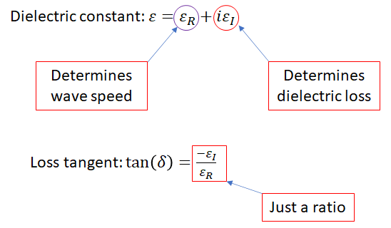
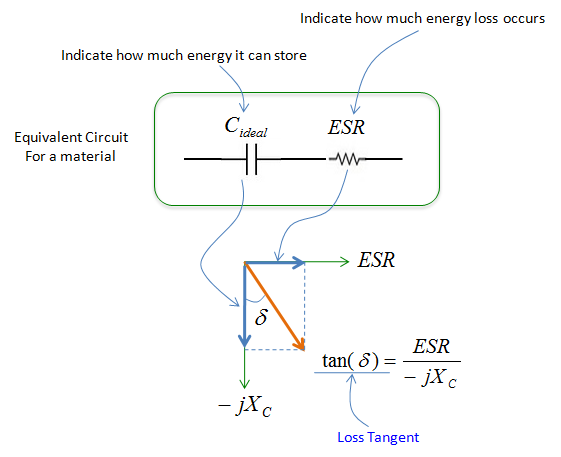
Loss tangent (Df) defines dielectric loss, but DK variation introduces mismatch loss. When impedance deviates from the intended value, part of the RF signal reflects back toward the source, reducing forward transmission.
Effects include:
- higher insertion loss
- increased ripple in filters
- degraded VSWR
- phase errors in antenna arrays
- unwanted standing waves
Stable DK helps avoid these issues by keeping impedance as close as possible to its original design target.
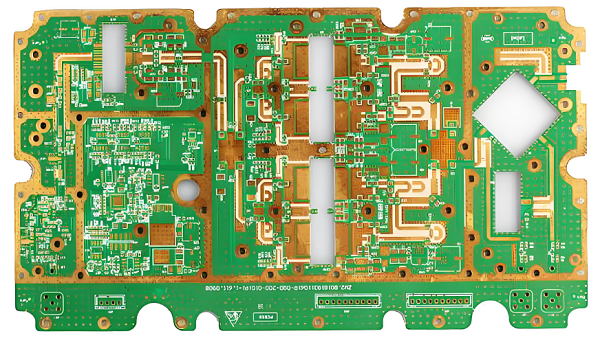
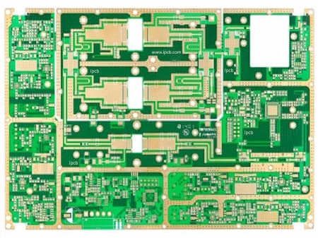
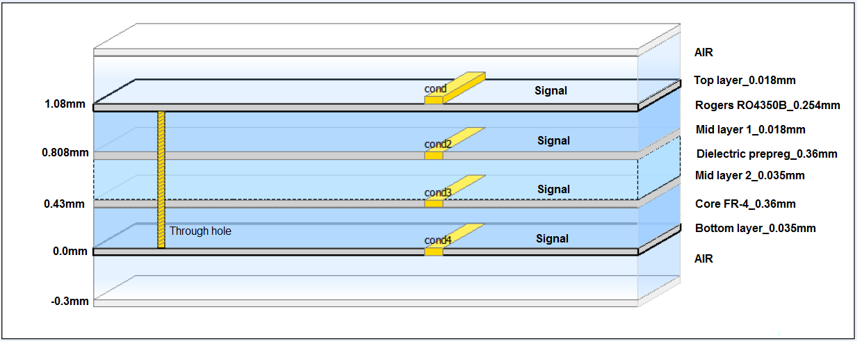
DK and RF PCB Stack-Up Selection
A high-performance RF PCB stack-up design always begins with DK. Engineers set copper thickness, dielectric thickness, and trace geometry around it. RF stack-ups with predictable DK behave consistently across production batches, which keeps high-volume runs stable.
Popular RF materials selected for stable DK include:
- Rogers RO3003 (DK ≈ 3.00 ± 0.04)
- Rogers RO4350B (DK ≈ 3.48 ± 0.05)
- Rogers RO4003C (DK ≈ 3.38 ± 0.05)
- Rogers RO5880 (DK ≈ 2.20 ± 0.02)
- Taconic RF-35, TLY, and other PTFE-based laminates
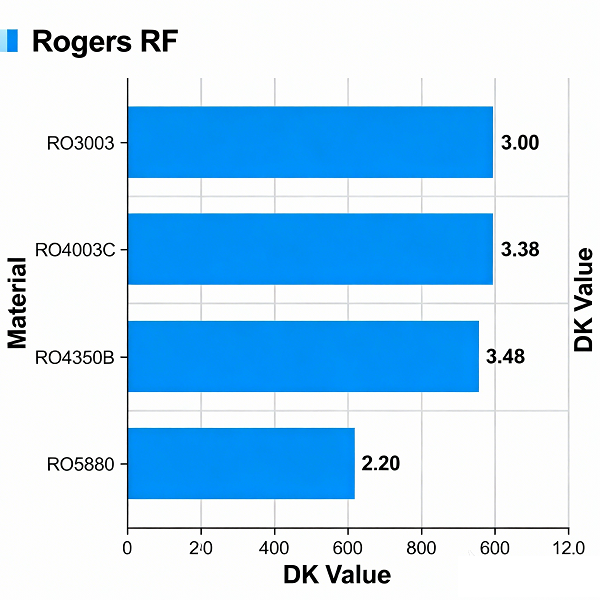
These laminates are widely used in microwave designs because they give designers the confidence that impedance and electrical length stay predictable across builds.
Why DK Matters Even More Above 10 GHz?
As frequencies extend toward mmWave ranges, minor DK deviations introduce major impedance shifts. The higher the operating frequency, the more sensitive impedance becomes to dielectric constant variations.
For example:
- At 1–2 GHz, DK tolerance of ±0.05 produces measurable but manageable impact.
- At 10–24 GHz, the same DK deviation causes more dramatic impedance changes.
- Above 28–39 GHz (5G FR2 bands), DK control becomes one of the most essential parameters in RF material selection.
This is why mmWave PCB manufacturing overwhelmingly relies on PTFE-based or ceramic-filled laminates with extremely tight DK tolerance.
EBest Circuit (Best Technology) – Your Trusted Partner for RF PCB Manufacturing
For designers working on high-frequency and microwave projects, precise DK control is only the starting point. You also need a PCB manufacturer with strong RF engineering experience, stable processes, and a deep understanding of controlled impedance PCB builds. At EBest Circuit (Best Technology), we support global RF teams through:
1. Advanced RF PCB materials – RO3003, RO4350B, RO4003C, RO5880, Taconic, and other high-frequency laminates.
2. Tight impedance tolerance – ±5% impedance control with certified test reports.
3. Professional RF stack-up design assistance – Our engineers help calculate trace widths, dielectric thicknesses, and Dk_eff models for accurate impedance.
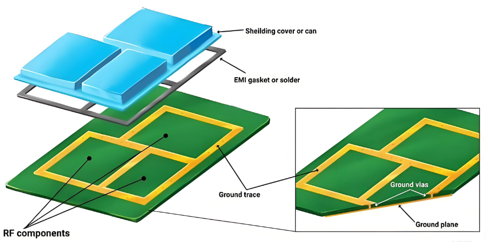
4. Mature RF PCB fabrication capabilities – Microstrip, stripline, CPW, grounded CPW, hybrid stack-ups, cavity structures, and metal-backed RF boards.
5. Rigid quality control – ISO9001, ISO13485, AS9100D, IATF16949, and full MES traceability for all builds.
When your RF design demands precise signal behavior, stable impedance, and reliable material performance, EBest Circuit (Best Technology) provides the expertise and manufacturing strength needed to support advanced RF and microwave innovation.