Choosing the right manufacturing model is one of the most important strategic decisions for electronics companies. In the PCB and PCBA sector, product lifecycles are shorter, technical requirements are higher, and global competition is stronger than ever. In this environment, two models, OEM and ODM, shape how your boards move from idea to mass production.
This guide explains both models in clear terms, compares them using real PCB scenarios, and provides a practical decision framework that engineers, buyers, and founders can use when planning their next PCB or PCBA project.
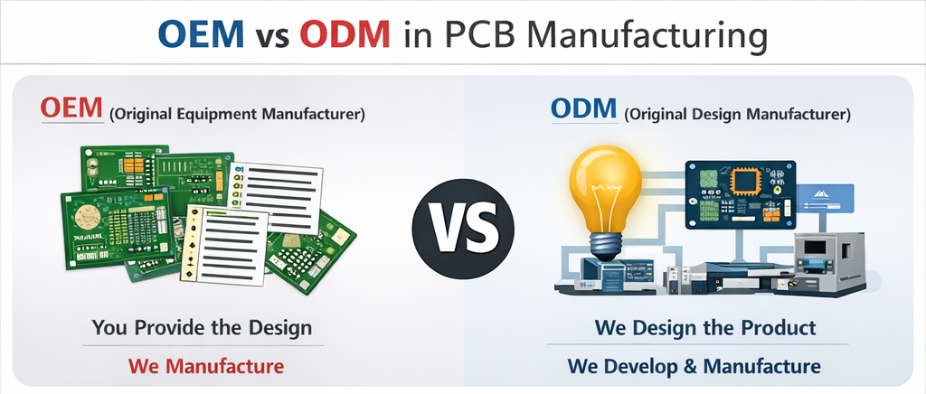
What Is OEM Manufacturing in the PCB Industry?
OEM manufacturing refers to a model where the customer owns the product design, controls the technical specifications, and provides the documentation needed for production. In the PCB field, an OEM project usually includes:
- Complete Gerber files and drill files
- Stack-up information and layer count definition
- Bill of materials (BOM) with approved vendor list
- Assembly drawings and mechanical constraints
- Testing procedures and acceptance criteria
- Quality and reliability requirements
Under the OEM model, the PCB manufacturer acts as a specialist executor. The factory fabricates boards,
assembles components, and runs tests in strict alignment with the customer’s design and documentation.
The engineering ownership remains on the customer side, while the manufacturer delivers robust production, process control, and supply chain support.
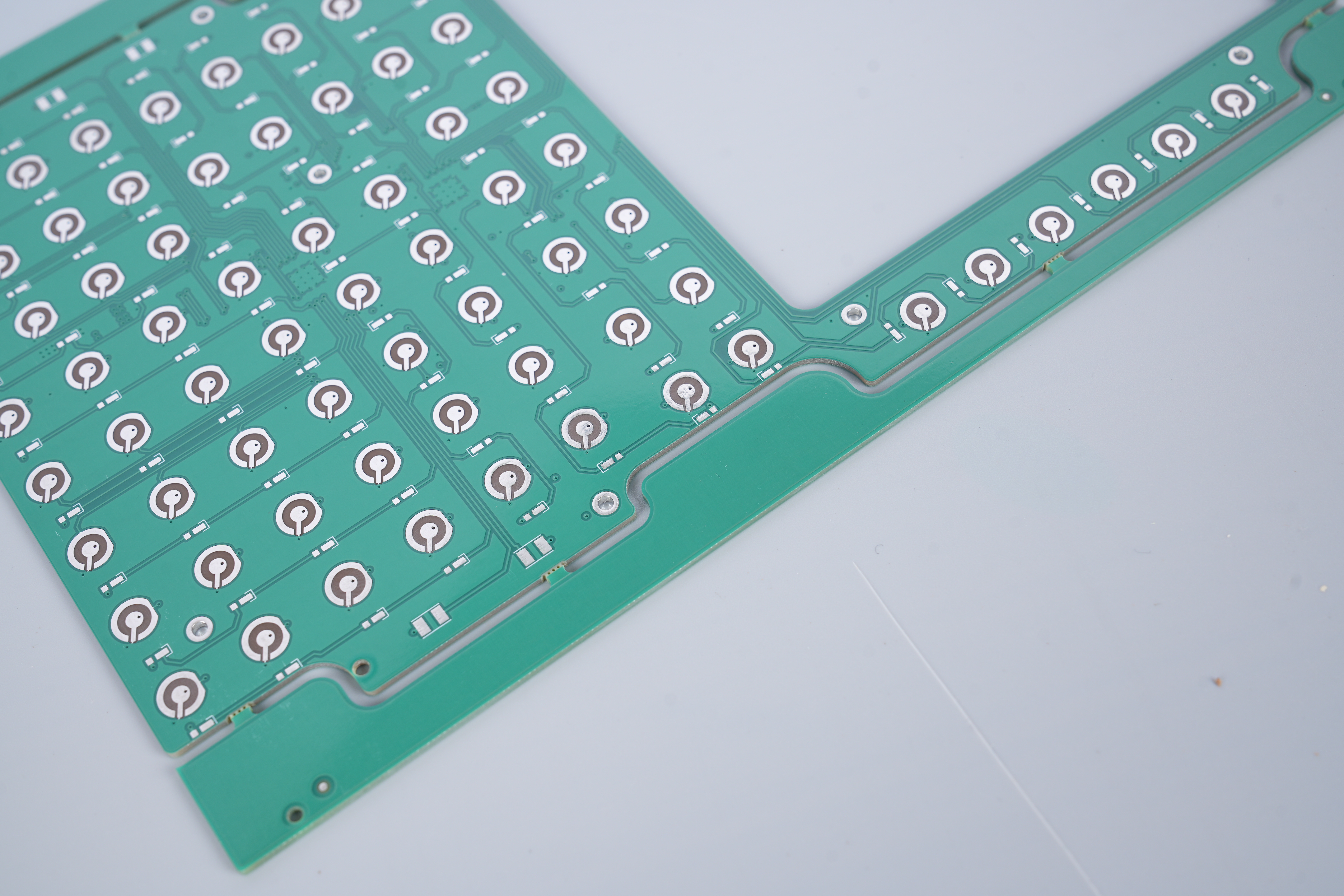
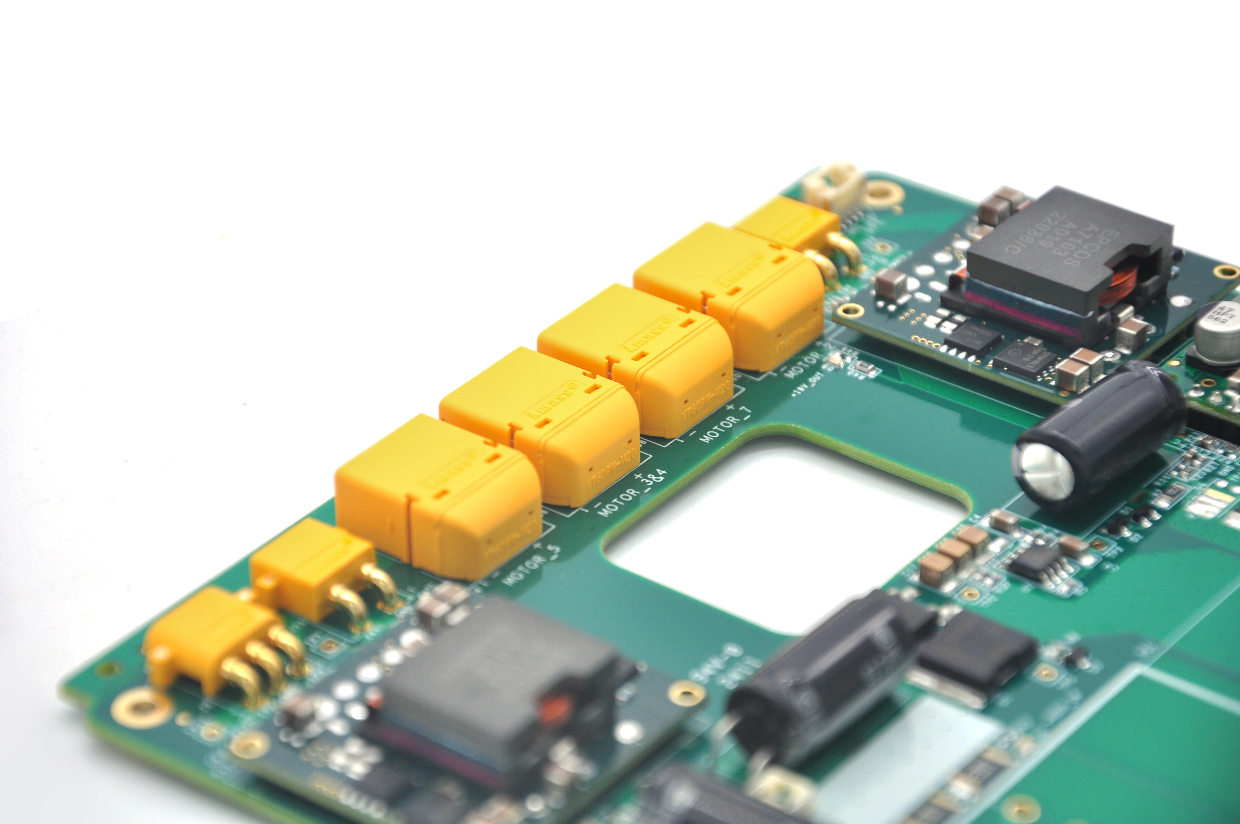
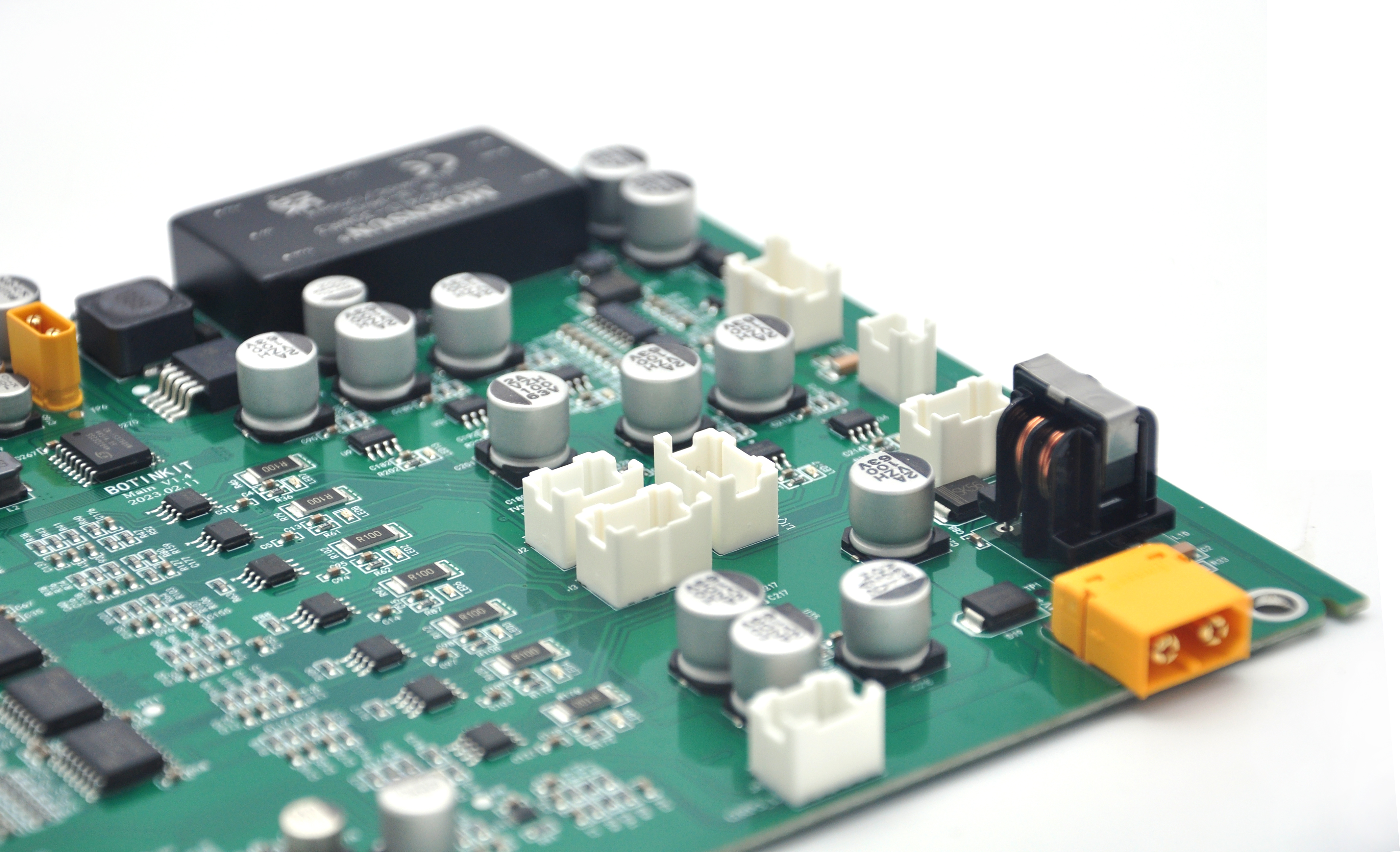
In the PCB industry, OEM manufacturing is common in fields where design control and traceability matter:
- Medical instrumentation and life-support electronics
- Automotive electronics and ADAS-related boards
- Aerospace and defense control modules
- High-frequency RF and microwave PCBs
- Industrial automation controllers
- Robotics and motion control systems
These applications often involve tight regulations, proprietary algorithms, and long-term maintenance. Companies choose the OEM path because it allows them to keep full control of their PCB design while relying on an experienced manufacturing partner for fabrication, assembly, and testing.
What Is ODM Manufacturing in the PCB Industry?
ODM manufacturing goes beyond production and includes design and development. Instead of providing a finished design, the customer shares functional requirements, performance targets, and budget expectations. The ODM manufacturer then handles engineering and turns the requirements into a manufacturable PCB or PCBA solution.
Typical ODM services in the PCB domain include:
- Circuit concept and schematic design
- PCB layout and stack-up planning
- Component selection and alternative sourcing
- Design for manufacturability (DFM) and design for assembly (DFA)
- Prototype build and design iterations
- Compliance support and basic certification guidance
- Full-scale production and functional testing
Many growing electronics brands, start-ups, and non-technical founders choose ODM when they need a finished PCB solution but do not have sufficient internal engineering resources. The manufacturer becomes both a design partner and a production partner.
In the PCB and PCBA world, ODM is frequently used for:
- IoT sensor nodes and gateways
- Smart home and building automation devices
- Wearable electronics and fitness trackers
- LED lighting drivers and control boards
- Consumer electronics modules and controller boards
- Low-power wireless communication boards
These market segments evolve quickly and demand frequent updates. A capable ODM PCB partner can speed up development and help clients get new boards into the market much faster.
OEM vs ODM: Core Differences for PCB and PCBA Projects
Both OEM and ODM are valuable, but they solve different problems. Understanding how they
differ helps you select the model that fits your product, budget, and timeline.
| Area | OEM | ODM |
|---|---|---|
| Design Ownership | Customer owns design, files, and IP | Manufacturer often owns design unless transferred by contract |
| Development Cost | Lower upfront design cost, higher internal engineering investment | Higher upfront design charge, reduced internal engineering load |
| Time to Market | Depends on customer’s design speed | Shorter due to in-house design resources and templates |
| Engineering Support | Focused on DFM, DFA, and production advice | Full design plus optimization support |
| MOQ Flexibility | Often higher for mature products | Can be lower for pilot and first launches |
| Customization Level | Unlimited customization within process capability | Often based on existing platforms or reference designs |
| IP Protection | Very strong, assuming secure data handling | Contract-dependent; must be clearly defined |
| Risk Profile | Lower in production, higher in internal design quality | Lower design risk, but higher IP and dependency risk |
Engineers often pick the OEM route when they need tight control over design, especially for high-end or
regulated PCBs. Teams that prioritize speed, flexibility, and reduced internal workload tend to lean toward ODM.
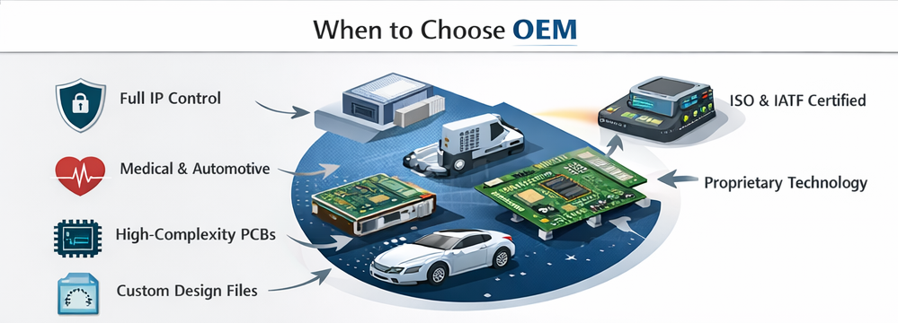
When Should a PCB Company Choose OEM?
The OEM manufacturing model is ideal when technical control, long-term stability, and full customization
are your highest priorities.
You should prefer OEM when:
- You already have a PCB design or a strong internal R&D and layout team.
- Your product must comply with strict standards such as ISO 13485, IATF 16949, or specific medical or automotive norms.
- You handle sensitive RF front-ends, custom impedance structures, or advanced HDI designs.
- You plan to maintain and update your product over many years.
- You want full freedom to switch manufacturers while keeping the same design.
In these situations, working with an experienced OEM PCB partner gives you manufacturing stability while you retain all core design decisions. This model suits companies that treat their PCB design as a central asset in their business.
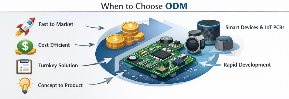
When Is ODM the Better Option for PCB Projects?
The ODM model is a better fit when you care most about speed, simplified development, and reduced engineering overhead.
Consider ODM when:
- You have a clear product idea but no detailed PCB design.
- Your team lacks time or skills to manage schematics and layout.
- You want to test a new market quickly and validate demand with a working prototype.
- Your project falls into categories with fast refresh cycles, such as IoT or consumer electronics.
- You prefer a one-stop solution from concept through production and assembly.
An experienced ODM PCB partner can turn functional requirements into a board design, prototype it, optimize for manufacturing, and ramp into production. This is especially valuable for start-ups and smaller brands that want to focus more on marketing and sales while outsourcing technical development.
OEM and ODM Pricing Models and Cost Drivers in PCB Manufacturing
Both OEM and ODM projects are influenced by similar manufacturing cost factors, but their
structures differ at the development stage.
Key Cost Drivers for OEM PCB Projects
- Base material type (standard FR4, high-Tg, Rogers, ceramic, metal-core)
- Layer count, board thickness, and stack-up complexity
- Trace width and spacing, especially in HDI designs
- Via types (through-hole, buried, blind, microvias)
- Surface finish (HASL, ENIG, immersion silver, OSP, ENEPIG)
- Component mix, package density, and assembly complexity
- Testing coverage (ICT, flying probe, functional test)
- Yield targets and reliability expectations
- Logistics, packaging, and shipping requirements
In OEM projects, design work is already complete, so development cost is mainly related to DFM review and minor adjustments. The main financial focus is on fabrication, assembly, materials, and testing.
Key Cost Drivers for ODM PCB Projects
- Concept definition and hardware architecture
- Schematic capture and simulation if required
- PCB layout and optimization cycles
- Prototype iterations and validation builds
- Component selection, sourcing, and second-source planning
- Compliance support and pre-certification testing where needed
In ODM projects, you pay for additional engineering work in exchange for a much lighter internal workload and a faster path to a finished board. The overall cost can be very competitive when you consider the time saved and the opportunity to reach the market earlier.
How to Protect Your IP with OEM and ODM PCB Partners
Intellectual property protection is one of the most sensitive topics when companies decide between OEM and ODM. While no model is completely risk-free, there are practical steps that significantly reduce exposure.
- Formal NDAs and Manufacturing Agreements: Clearly define confidentiality around schematics, Gerber files, BOM, firmware, and test tools.
- Contractual IP Ownership: In ODM projects, specify whether IP will be transferred, shared, or licensed.
- Controlled File Sharing: Limit sensitive design information to dedicated engineering contacts.
- Firmware Protection: Use secure bootloaders, encryption, and lock bits for microcontrollers when needed.
- Selection of Certified Partners: Choose factories with ISO and industry-specific certifications that follow disciplined processes.
With a solid legal framework and careful partner selection, both OEM and ODM collaborations
can support long-term, secure PCB programs.
Quality Control Strategies for OEM and ODM PCB Production
Reliable PCB performance comes from consistent process control, not only from design quality. A professional PCB supplier, whether working under an OEM or ODM model, should implement a systematic quality strategy.
- Incoming quality control (IQC) for copper clad laminates, solder paste, and components
- In-process checks (IPQC) at critical stages such as etching, drilling, plating, and soldering
- Automated optical inspection (AOI) for bare boards and assembled boards
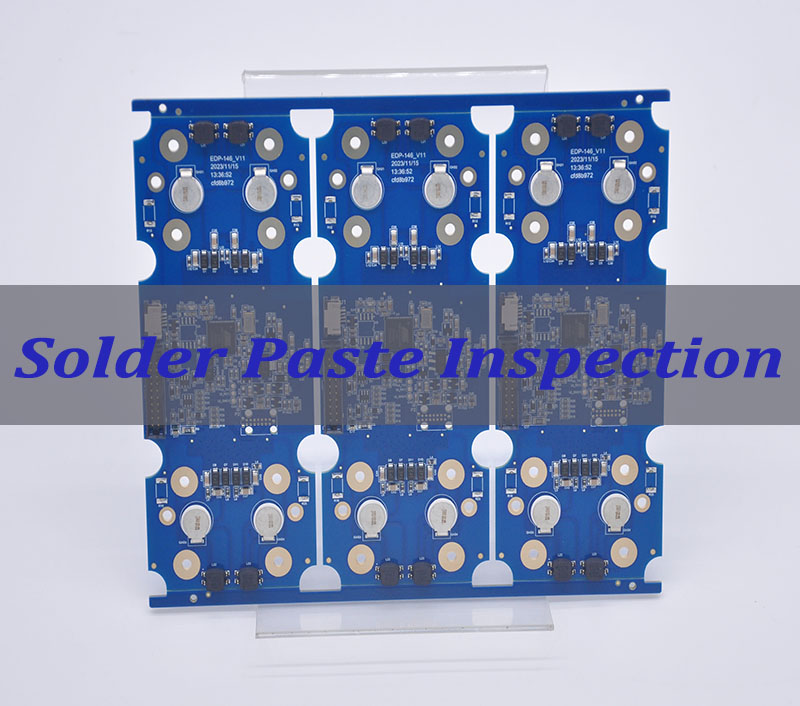
- Solder paste inspection (SPI) for SMT process control
- X-ray inspection for BGA, QFN, and hidden joints
- Electrical tests (flying probe or ICT) for open and short detection
- Functional tests and burn-in for mission-critical products
In ODM projects, additional validation is often required at the prototype stage, because the design is fresh. In OEM projects, focus is more on maintaining stable yields and repeatability once the design is frozen.
How to Evaluate and Select a Reliable OEM or ODM PCB Supplier
Selecting your manufacturing partner is a decision that affects product quality, lead time, cost, and even brand reputation. Whether you prefer OEM or ODM, certain evaluation points remain essential.
- Engineering Capability: Can the supplier handle HDI, RF, flex, rigid-flex, ceramic, or heavy copper boards?
- DFM and DFA Support: Do they proactively optimize your design for yield and manufacturability?
- In-house SMT and Assembly: One-stop fabrication and PCBA in locations such as China and Vietnam improves coordination.
- Certifications: Look for ISO 9001, ISO 13485, IATF 16949, and UL where relevant.
- Equipment Level: Advanced drilling, imaging, solder mask, SPI, AOI, and reflow lines reflect process strength.
- Prototype and Low-volume Capability: This is vital for early-stage ODM projects and design validation.
- Communication and Project Management: Clear, responsive communication reduces delays and misunderstandings.
A strong PCB partner is more than a factory. It should be a technical advisor that helps you reduce risk and increase reliability.
OEM and ODM Examples Across PCB-Intensive Industries
Both OEM and ODM models are widely used across industries that rely heavily on PCBs and
assembled boards.
Typical OEM PCB Applications
- Medical diagnostics and laboratory equipment PCBs
- Industrial motion control and PLC boards
- Automotive control modules and sensor interfaces
- High-speed communication backbone boards
- Ceramic-based power modules for power electronics
Typical ODM PCB Applications
- Smart home controllers and gateways
- IoT sensor nodes and tracking devices
- Wearable health monitors
- LED lighting drivers and control PCBs
- Compact consumer product controller boards
These examples show that both models are valid tools. The choice is not about which one is absolutely better, but about which
one matches your product and business goals.
FAQs: OEM and ODM for PCB and PCBA
Below are some of the most common questions engineers, buyers, and founders ask when comparing OEM and ODM in the PCB domain.
Q1. Is OEM always more expensive than ODM?
Not always. OEM projects can be cost-effective when you already have a mature design and stable volume. ODM includes engineering fees, but it saves internal R&D cost and time. The better option depends on how much design work you can handle in-house.
Q2. Do I keep my IP if I work with an ODM supplier?
IP ownership in ODM projects depends on the contract. Some suppliers transfer full design ownership to you, while others retain partial rights. Make sure ownership, licensing, and future use of the design are clearly described in your agreement.
Q3. What is the typical MOQ difference between OEM and ODM?
OEM projects often have higher MOQs because they support stable, long-term products. ODM suppliers sometimes offer lower MOQs for pilot runs or market testing, especially in consumer and IoT sectors.
Q4. Can I start with an ODM design and later move to an OEM model?
Yes. Many companies use ODM to launch fast, then move to an OEM model with a custom design once
the market is proven. Carefully plan IP and file access from the start to keep this option open.
Q5. Which model is better for highly specialized or high-reliability PCBs?
For complex HDI, RF, high-speed, or safety-critical boards, OEM is usually the stronger choice. You maintain full design control and can work with a manufacturer that focuses on process excellence and reliability.
Q6. Which model helps us launch faster?
ODM typically shortens launch time because design, layout, and prototyping are handled by the manufacturer. If speed and reduced internal workload are top priorities, this model offers a practical shortcut.
How to Decide Between OEM and ODM for Your Next PCB Project?
Deciding between OEM and ODM is easier when you look at your situation through three lenses:
technical control, available resources, and time to market.
Choose OEM if you:
- Have or plan to build internal PCB design expertise.
- Need strict IP control for competitive or regulated products.
- Expect long product lifecycles and multiple future revisions.
- Work in medical, automotive, aerospace, or other high-reliability areas.
Choose ODM if you:
- Want to turn a product concept into a ready PCB quickly.
- Prefer to outsource heavy engineering work.
- Operate in fast-changing consumer or IoT markets.
- Need a one-stop partner for design, fabrication, assembly, and testing.
In practice, many companies use both models at different stages. They may rely on ODM partners for early concepts and market tests, then shift to an OEM model once volumes grow and the product stabilizes. By matching the model to each development phase, you can control cost, manage risk, and keep your roadmap flexible.