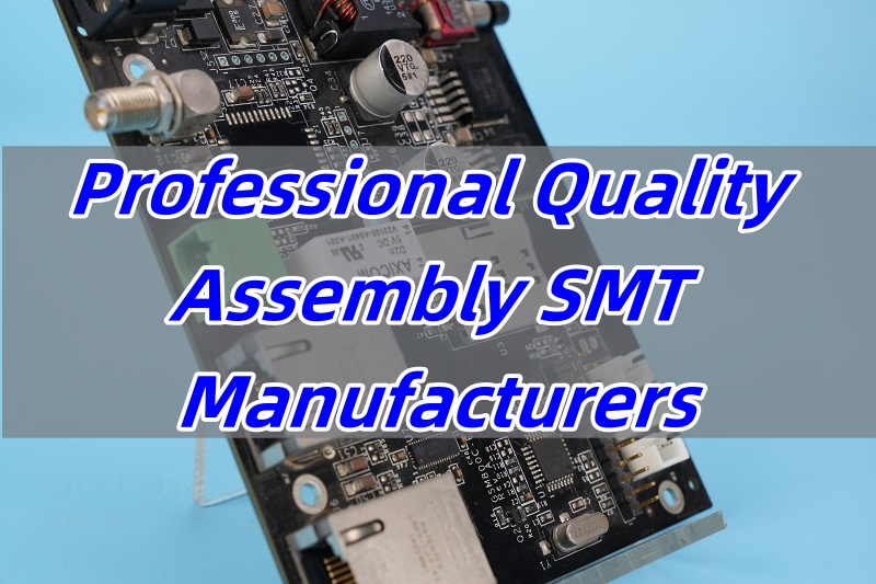
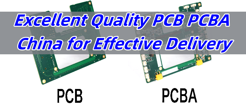
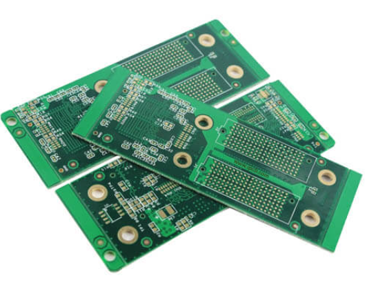
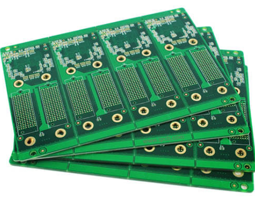
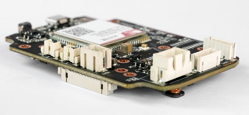
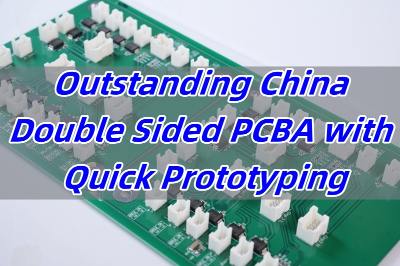
China double sided PCBA has become a reliable choice for industries that require both quality and speed. From aerospace to consumer electronics, this solution supports fast development without compromising on performance. With growing global demand, China remains the top supplier of double-sided PCBAs due to advanced equipment, skilled engineering, and optimized costs.
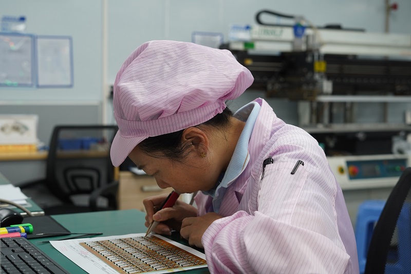
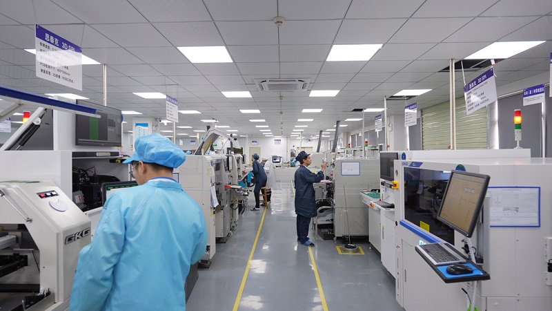
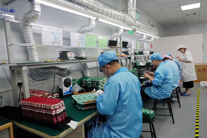
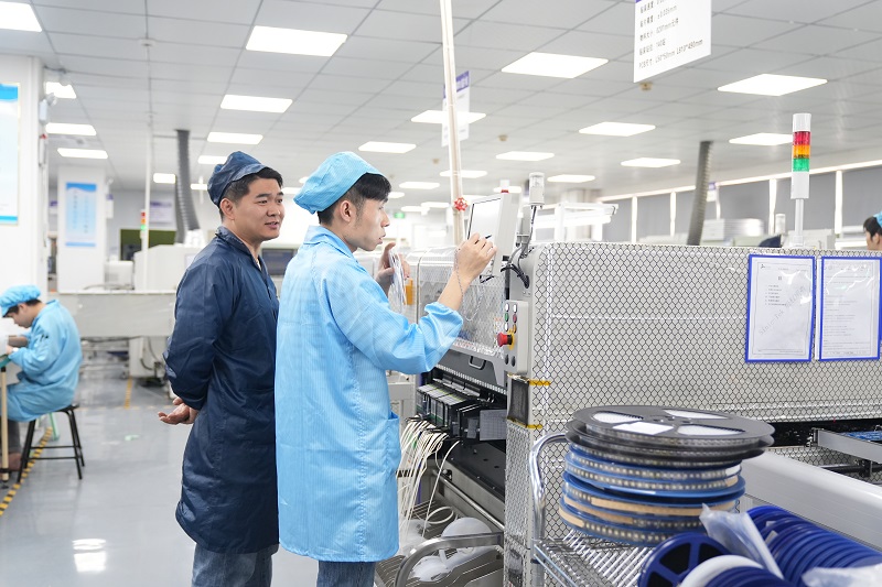
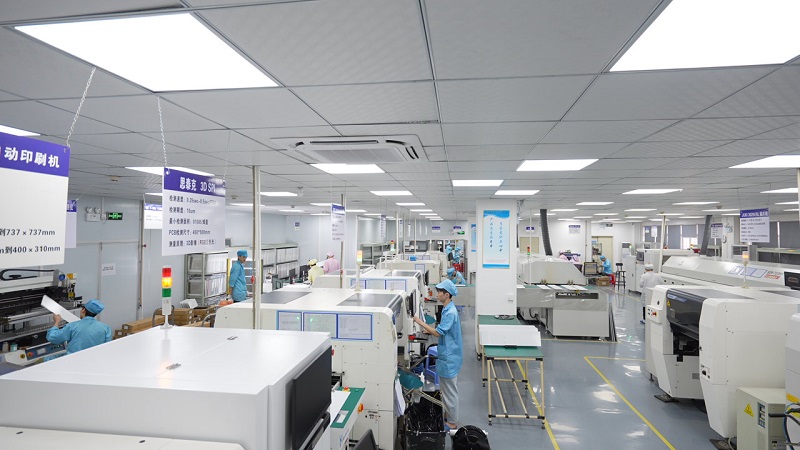
EBest Circuit (Best Technology) offers outstanding China double sided PCBA with quick prototyping service in the globally competitive market. There are around 10 engineers in our R&D department, most of whom have more than 10 years of experience. And we provide well-focused training for all staff regularly. Our PCBA factory has the qualifications and ability to handle your projects and give you workable solutions under varying conditions, including but not limited to specialized processes such as high-density boards, flex boards, and high-speed signal boards. Please share the BOM list, SMT placement coordinates, and RefDes silkscreen layer with us at sales@bestpcbs.com to get a free quote.
Which Type of PCB Has Conductive Paths on Both Sides?
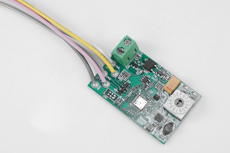
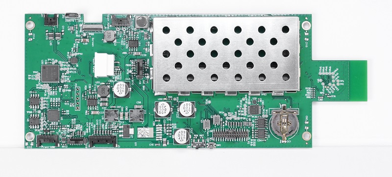
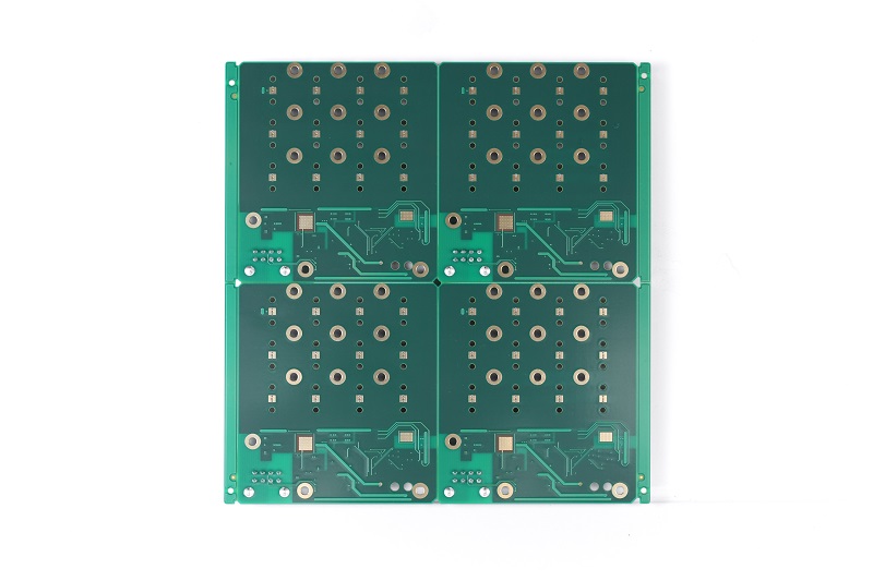
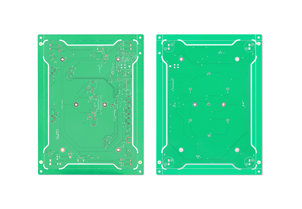
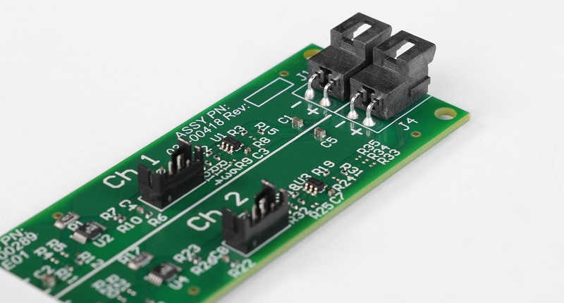
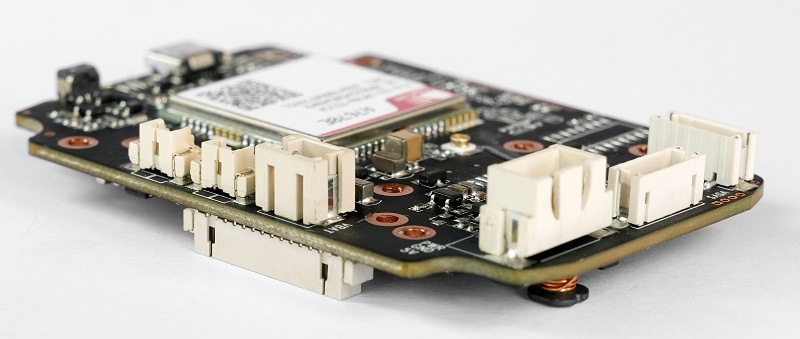
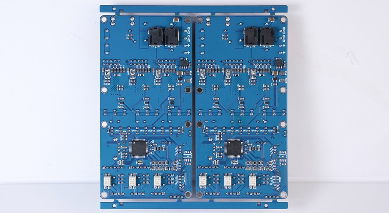
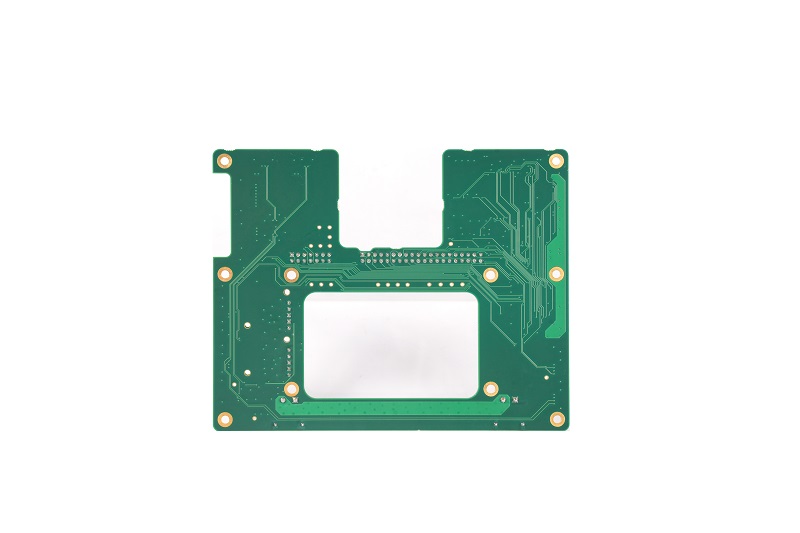
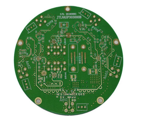
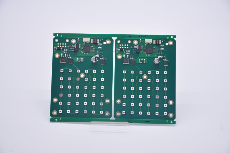
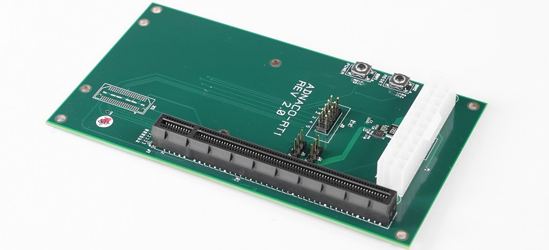
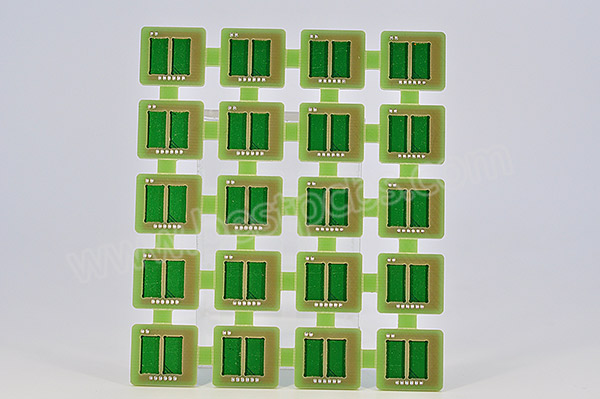
Double-sided PCBs have conductive paths on both sides of the board. These paths allow more complex circuits in compact spaces. Vias connect the top and bottom layers, enabling signal flow across both surfaces. This structure supports a wider range of designs compared to single-sided PCBs, especially in multi-functional electronic devices.
What is the Difference Between Single-Sided and Double-Sided PCBA?
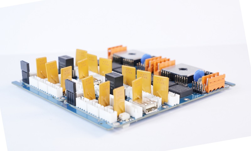
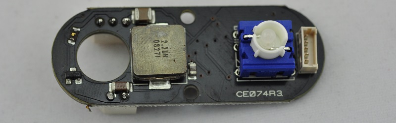
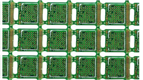
The key difference lies in the number of copper layers. A single-sided PCBA has components and traces only on one side, making it simpler and cheaper. Double-sided PCBA, however, has traces and components on both sides. It handles more complex circuits and higher component density. Despite being costlier, it offers more functionality for high-performance products.
Who Is the Best Manufacturer of China Double Sided PCBA?
Among many Chinese manufacturers, EBest Circuit (Best Technology) stands out for its professional and complete solution services. With certifications like ISO 9001, ISO 13485, IATF 16949, and AS9100D, it meets quality standards across critical industries. The team provides 24/7 technical support, and their MES system ensures full traceability. EBest Circuit (Best Technology) provides double-sided PCBA manufacturing services to clients in the medical, automotive, and aerospace industries, meeting their requirements for reliable circuit board solutions.
How Much Does a China Double Sided PCBA Cost?
The cost of China double sided PCBA depends on several factors such as board size, component complexity, materials, and volume. FR-4 remains the most common material due to its cost-effectiveness. However, advanced applications might require enhanced materials. EBest Circuit (Best Technology) helps reduce costs by optimizing yield rates, selecting proper materials, and streamlining processes. This ensures competitive pricing, even for small batches.
How Are Double-Sided PCBA Soldered?
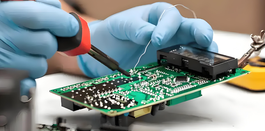
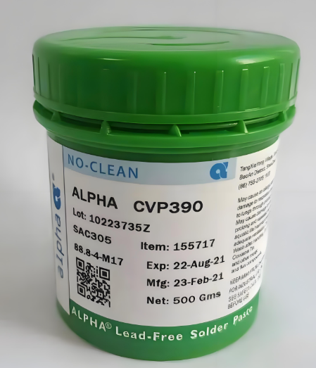
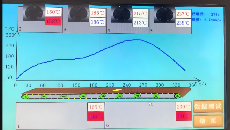
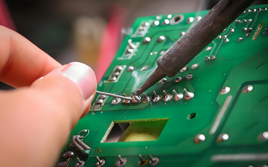
Soldering in double-sided PCBA typically involves reflow soldering on both sides. Components on one side are soldered, then the board is flipped to process the other side. Selective wave soldering might be used for through-hole parts. At EBest Circuit (Best Technology), precise control of temperature and time helps avoid issues like cold joints or bridging. AOI and X-ray inspections further verify the solder quality.
How to Make Double-Sided PCBA?
Manufacturing a double-sided PCBA includes several steps:
- Design preparation with Gerber files
- PCB fabrication with vias and copper plating
- Solder mask and surface finishing (ENIG, OSP)
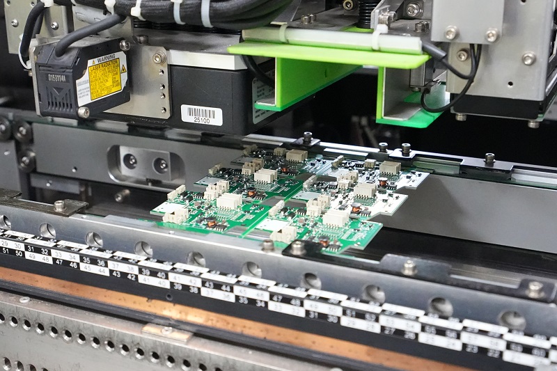
- Component placement using SMT machines
- Reflow soldering on each side
- Inspection through AOI and X-ray
- Function testing and final QA
At EBest Circuit (Best Technology), LDI technology helps speed up prototyping by 24-48 hours. This improves accuracy and shortens delivery time significantly.
What Are the Advantages of China Double Sided PCBA?
There are several benefits of choosing China double sided PCBA:
- High circuit density in small space
- Lower cost than multilayer PCBs
- Better performance and flexibility
- Fast prototyping and volume production
- Wide material and process options
With AI-driven LDI systems, EBest Circuit (Best Technology) improves accuracy while reducing defect rates. These innovations support industries that cannot afford downtime or defects, such as automotive and aerospace fields.
Why Choose EBest Circuit (Best Technology) for China Double Sided PCBA?
EBest Circuit (Best Technology) focuses on solving real needs. Quality issues like solder bridges or delamination are minimized using advanced soldering controls and high-end inspection tools. To match fast market cycles, our standard processes and parallel testing help reduce turnaround time. For cost control, their engineers assist in material selection and process reduction.
In terms of support, EBest Circuit (Best Technology) offers 7×24 hour service. From design optimization to after-sales support, every step is covered. Their engineers are trained to handle complex applications, and custom solutions are available when needed. This makes EBest Circuit (Best Technology) a one-stop manufacturer for both PCBs and full SMT PCBA services.
To summarize, China double sided PCBA is growing in demand across high-reliability industries. While challenges like quality control and fast prototyping remain, firms like EBest Circuit (Best Technology) are pushing the limits. With AI-enhanced LDI, strong material control, full traceability, and responsive service, they provide the tools and expertise needed to thrive in today’s market. Whether it’s a small prototype or a high-volume run, EBest Circuit (Best Technology) ensures speed, quality, and reliability every step of the way. Interested in learning more about us? Reach us via email at sales@bestpcbs.com.