Nowadays, PCBs became more and more important and you can see it in every electronic device. The PCB plays a critical role in our daily life. With circuit board, the device can power on and help to transmit signals, manage heat and perform electricity. A good PCB can help to improve the overall of your device. However, not all the PCBs are work good and within your expectable, you must know how to test it and ensure it enables a good performance. As an experienced PCB manufacturers in Asia, today we want to share with you how we test a PCB, and we try to use simple words to make you sense.
What is a printed circuit board?
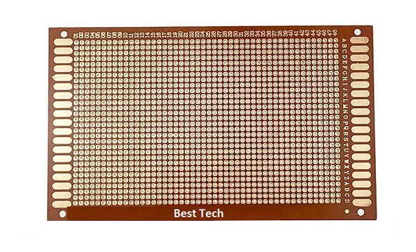
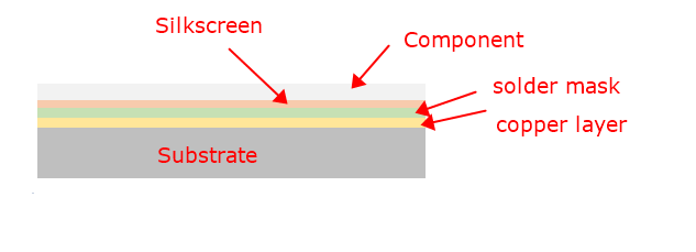
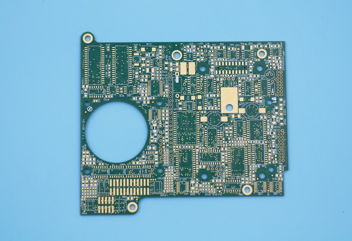
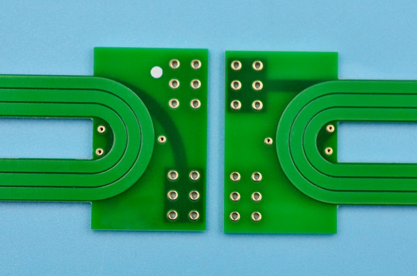
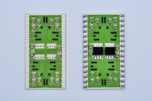
Before knowing the methods of testing circuit board, let’s understand the definition of PCB. A PCB is a flat board made from insulating materials like fiber glasses with conductive pathways etched onto its surface. The pathways we called circuit or traces. These pathways connect different electronic components, so that they can communicate and function together. PCBs come in various materials, shapes and sizes, which always is customized to meet specific applications and performance requirements.
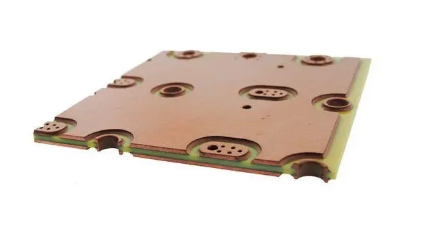
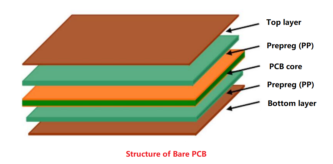
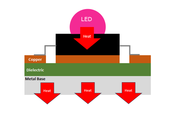
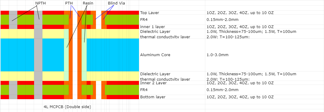
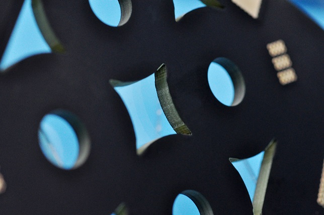
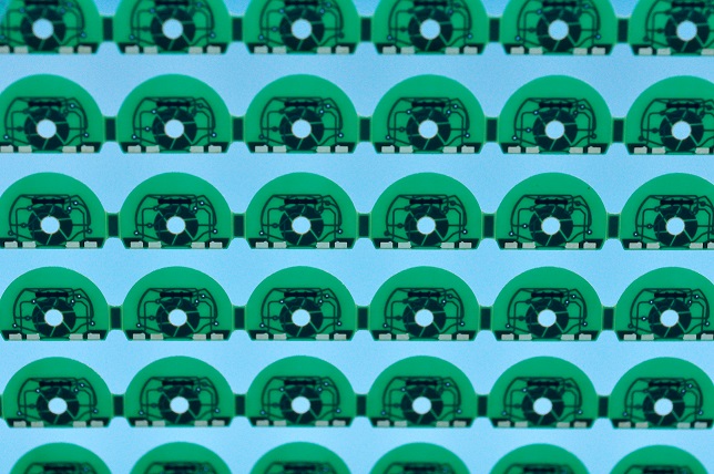
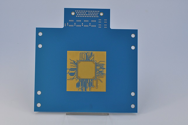
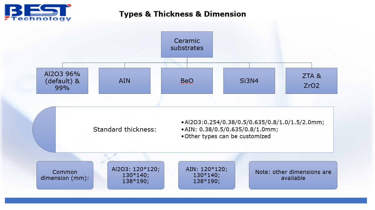
PCBs can be divided into different types according to substrate material used. They are – normal FR4 PCB, polyimide flexible PCB, metal core PCB, ceramic PCB, rogers PCB. Different has its own properties and advantages. The choice of materials and the design of the PCB significantly impact the performance and reliability of the final product. Understanding the materials used in PCBs is crucial for anyone involved in electronics, from hobbyists to professional engineers/designers.
Common PCB Circuit Board Issues
Though PCB has a strong construction, they are easy to be broken or failure since they always encounter a range of issues. These problems can stem from manufacturing defects, wear and tear, or improper handling. Identifying and diagnosing these issues promptly is crucial for maintaining the reliability and performance of electronic devices. Common issues we faced are including:
- Open Circuits: These occur when a break in the circuits prevents current flow normally. Open circuits can result from physical damage or manufacturing errors.
- Short Circuits: Due to improper soldering, unreasonable circuit design and other reasons, resulting in a short circuit between two or more points in the circuit that should not be connected. This can cause excessive current flow, potentially damaging components.
- Grounding: The unreasonable design of ground area leads to interference signals on the grounding, which affects the normal operation of the circuit.
- Signal: The signal circuit design is not reasonable, resulting in interference signals on the signal.
- Component Failures: Individual components on a PCB can fail due to aging, overheating, or electrical stress breakdown. And incorrect orientation will lead to the failure of PCB.
- Soldering Issues: Poor soldering can lead to weak connections, causing intermittent faults or complete circuit failure. This including the dents in the solder joints, this also can make the PCB failure.
- Corrosion: PCB exposure to moisture and contaminants for a long time can cause corrosion, degrading the conductive pathways and component leads.
How to check a PCB?
In generally, there are four common ways to check whether if your PCB are good or failure.
1. Visual inspection
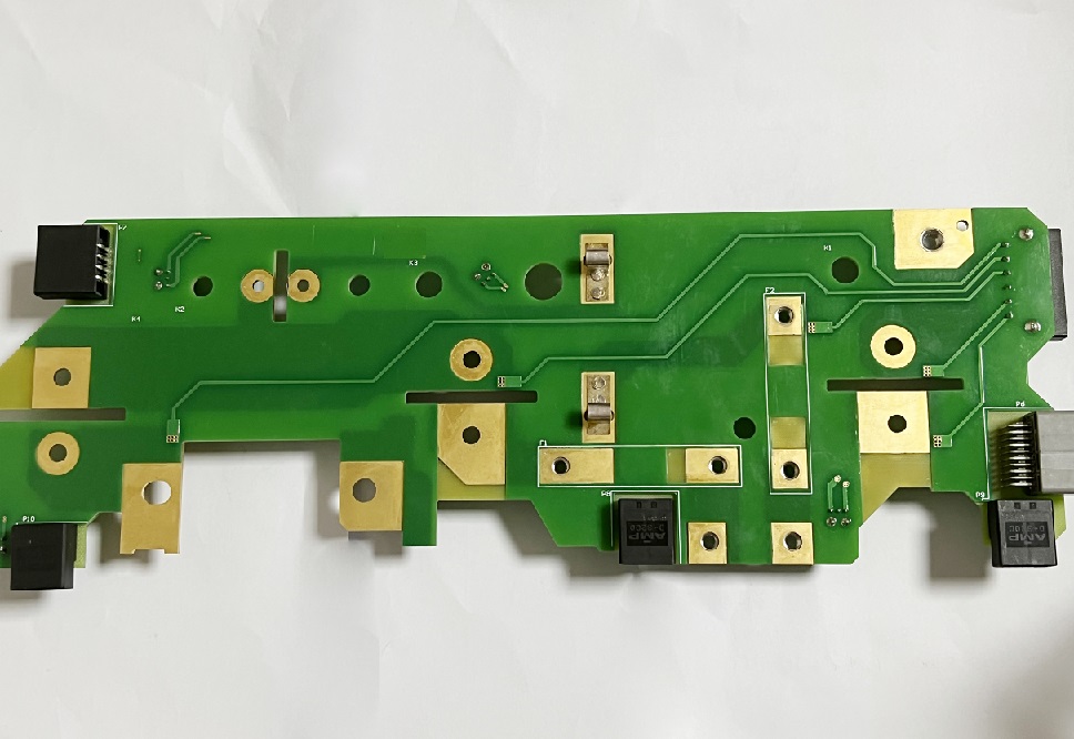
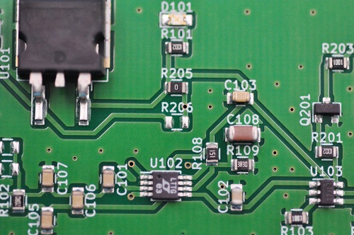
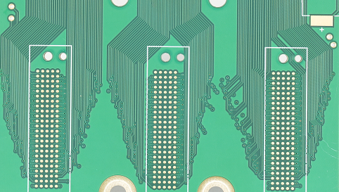
The easiest way is visual inspection. Through naked eye observation, check whether the solder joint on the PCB circuit board is firm, whether there is short circuit, open circuit and other phenomena. And look for burnt components, discolored areas, or broken traces, such as somewhere became black or be burned obviously. These are clear indicators of damage.
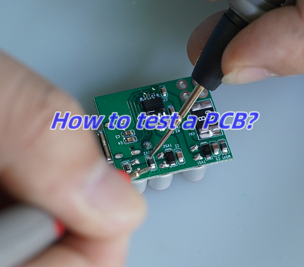
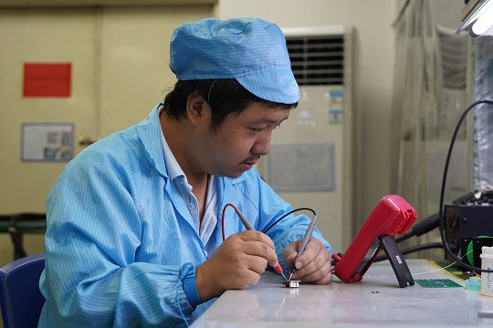
2. Use a multimeter
Multimeter is a common tool used for measuring PCB. Multimeter is versatility and it has multiplied modes. Select the appropriate mode on the multimeter, such as continuity, voltage, or resistance mode, depending on what you are testing. Before testing, make sure probes are in good condition and properly connected to the multimeter, with the red probe typically being positive and the black probe negative or ground. Click here to read What is the PCB flying probe test?
3. E-tester
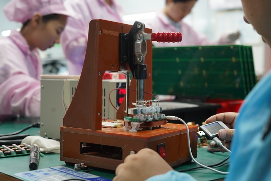
E-tester is a good way to test short or open circuit when it is a mass production. If you just want to test one piece PCB, multimeter is much better.
4. Use oscilloscope
An oscilloscope is a powerful diagnostic tool used to observe the waveform of electrical signals in a circuit. Connect the oscilloscope probes to the test points on the PCB, it can capture the waveform. By observing the waveform, determine whether the circuit is working normally.
5. Use a thermal imager
A thermal imager also is a effective way to check the condition of PCB. It can capture the temperature distribution on the PCB. It helps identify areas with excessive heat, which can indicate potential issues.
How to Test a Circuit Board with a Multimeter Effectively?
Testing a circuit board with a multimeter is essential for diagnosing and fixing electronic issues. A multimeter can measure voltage, current, and resistance, helping you identify problems with the PCB. The main way to test a PCB with a multimeter is to measure voltage, resistance, and ground.
- Measuring voltage
By measuring the voltage on the circuit board, can quickly test whether the circuit is working properly. Use the voltage gear of the multimeter, select the appropriate range, then measure the input and output of the power supply on the circuit board respectively, to check whether the voltage is within the normal range. If the voltage is abnormal, may indicate that the circuit is open or short.
- Measuring resistance value
By measuring the resistance value on the circuit board, can detect whether the circuit is smooth. Use the resistance level of the multimeter, select the appropriate range, then measure the key nodes on the circuit board, check whether the resistance value is within the normal range. If the resistance value is abnormal, may indicate that the circuit is open or short.
- Check the grounding
Grounding is critical to the proper operation of the circuit board. Use the multimeter’s ground test function, to check that key points on the board are properly grounded, this helps to spot potential electrical connection problems.
In addition, for industrial-grade PCB measurement, the use of higher-precision multimeters and special pens can improve the accuracy and efficiency of the measurement. For example, the Fluke 17B Max multimeter is equipped with an extra-pointed stylus, enables more accurate measurement of patch components and pins, and improves measurement fineness and accuracy.
Generally speaking, using a multimeter to test the PCB board needs to master the correct measurement methods and skills. At the same time according to the complexity of the circuit board to choose the appropriate measurement tools, to ensure the accuracy and efficiency of the test.
How to Tell if a Circuit Board is Bad?
Identifying a bad circuit board requires a combination of visual inspection and multimeter testing. Here are some signs and methods to determine if a PCB is faulty:
- Visual Signs
Look for burnt components, discolored areas, or broken traces, such as somewhere became black or be burned obviously. These are clear indicators of damage.
- Component Testing
Use the multimeter to test individual components. A component that doesn’t show the expected resistance or voltage is likely faulty.
- Continuity Testin
Check for open circuits. Lack of continuity in a path indicates a broken trace or solder joint.
- Short Circuit Detection
Identify any unintended connections between different paths. This can be done by checking for continuity where there should be none.
- Functionality Testing
Test the circuit board in its intended application. If the device does not function correctly, there may be an issue with the PCB.
Why Choose EBest Circuit (Best Technology)?
By reading this post, you may know how to test a PCB by multimeter already and other methods to identify them. EBest Circuit (Best Technology) has engaging in the PCB manufacturing for more than 18 years, we have served over 2000+ customers all around the world. We have strong R&D team and equipped with advanced equipment to improve the yield and product quality.
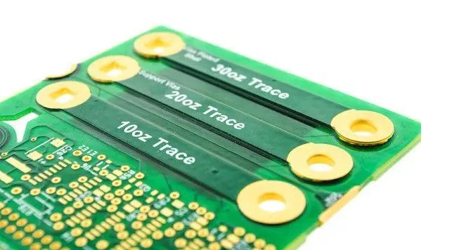
At EBest Circuit (Best Technology), we provide various PCB manufacturing, including metal core PCBs, ceramic PCBs, rigid-flex PCBs and some other special PCBs like HDI PCB, busbar PCB, heavy copper PCB. If you have similiar projects, you are welcome to contact us.