PCB manufacturing PCB manufacturing
Home > Blog

MCPCB prototype: What is Metal Core PCB?

February 21st, 2025

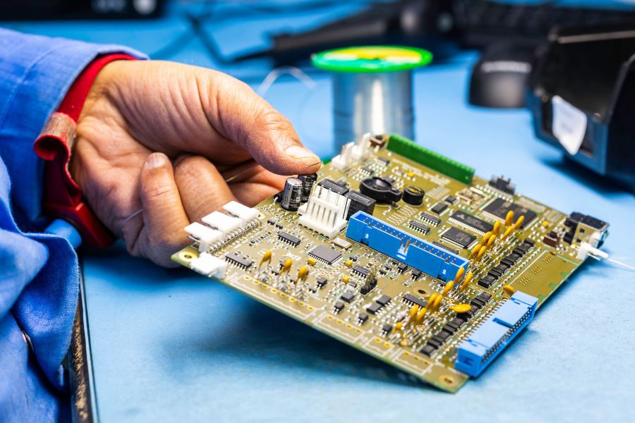
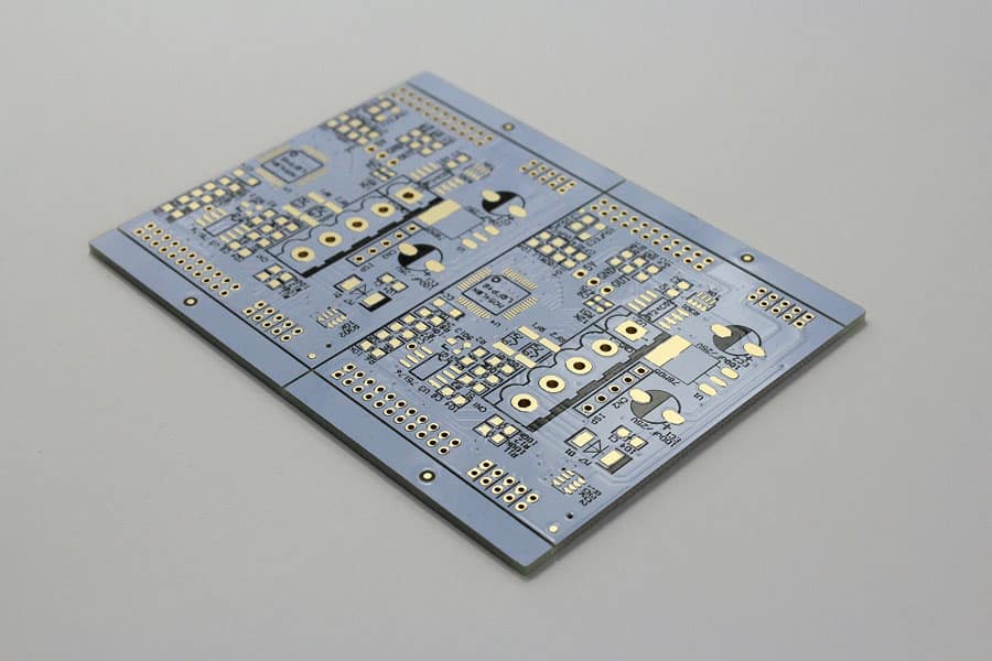
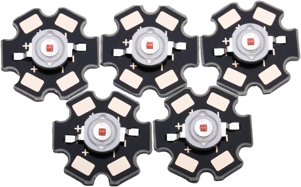
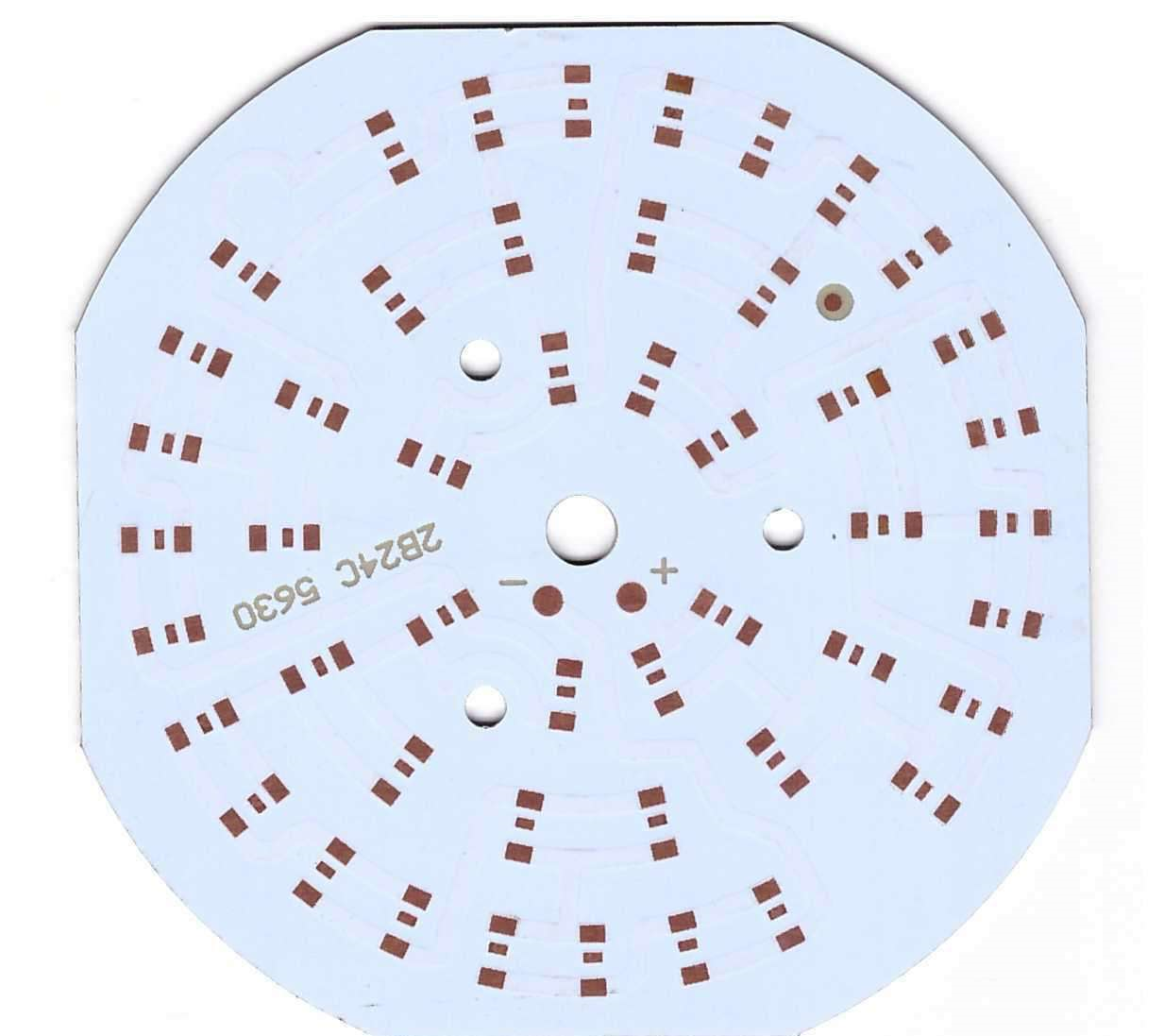
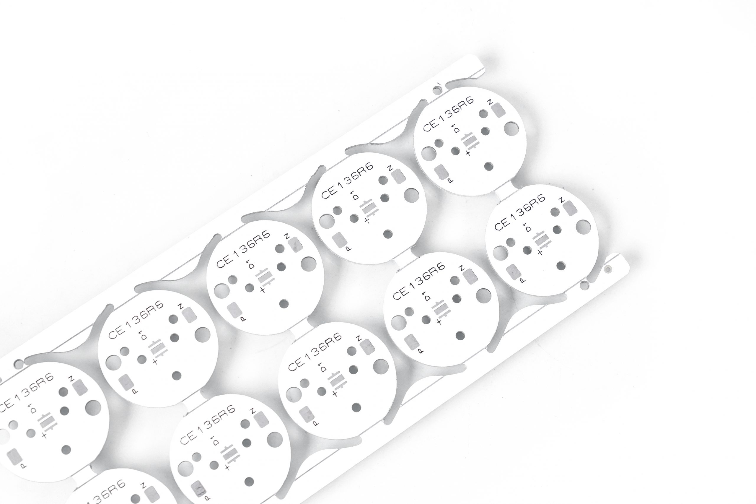
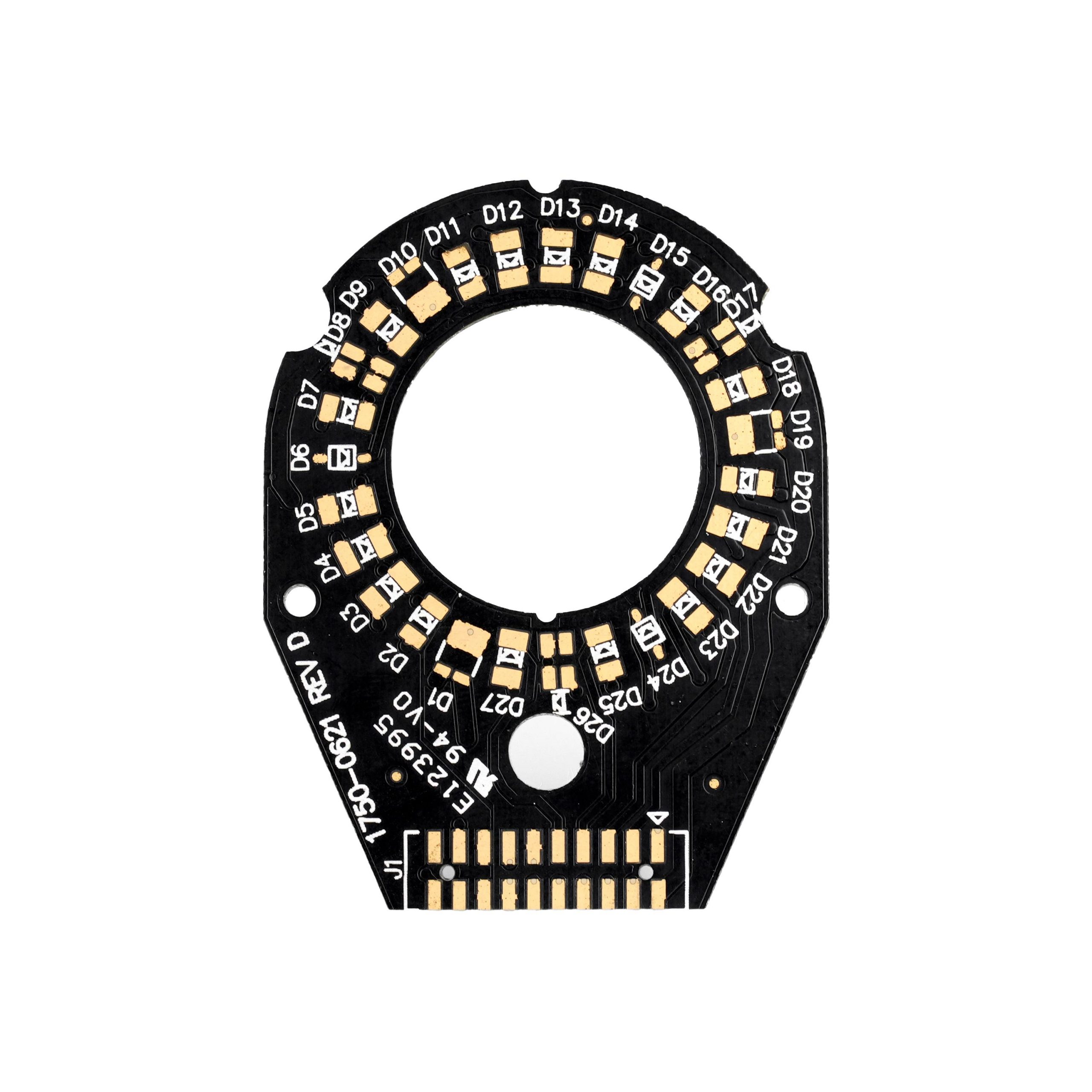
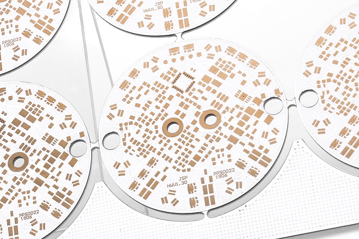
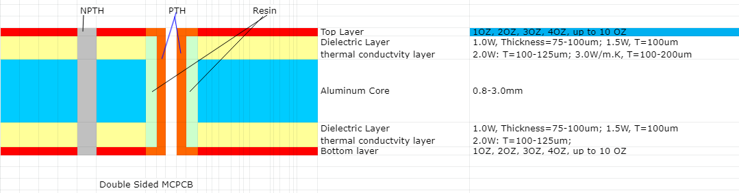
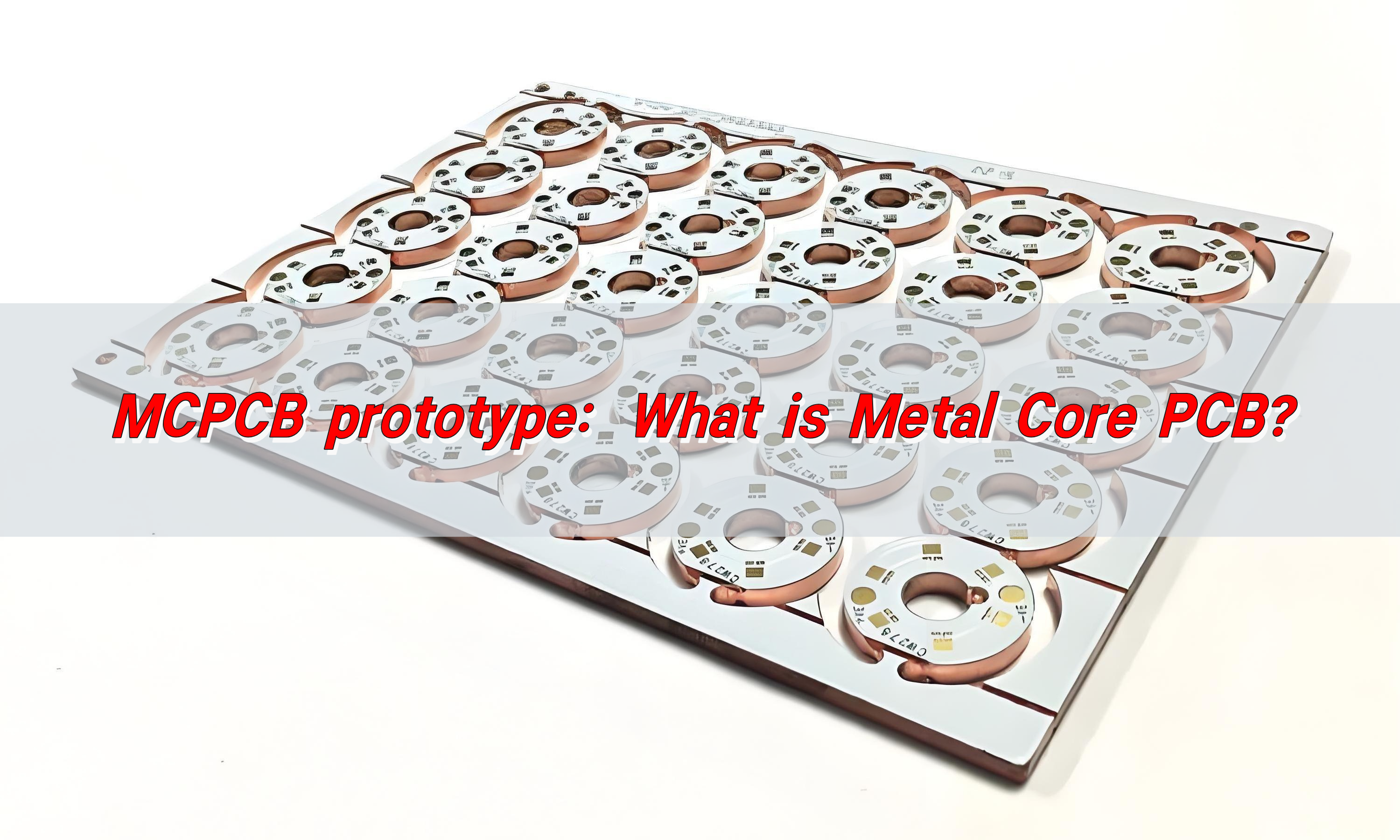
MCPCB prototype refers to Metal Core PCB. It consists of a metal substrate (such as aluminum or copper), an insulation layer, and a copper foil circuit layer. It has good heat dissipation performance and mechanical strength, and is suitable for high-power, high-heat dissipation demand application scenarios such as LED lighting, automotive electronics, and power management.

MCPCB prototype: What is Metal Core PCB?

What is mcpcb?

MCPCB stands for Metal Core Printed Circuit Board, a specialized type of PCB that includes a metal substrate instead of the traditional fiberglass (FR4) material. The purpose of the metal core is to improve heat transfer, ensuring that components operate within safe temperature limits.

In electronic devices that generate significant heat, such as high-power LEDs and automotive circuits, standard PCBs struggle with heat dissipation, leading to performance degradation and component failure. MCPCBs solve this issue by quickly transferring heat away from critical areas, maintaining optimal performance and extending product lifespan.

How to design mcpcb?

Designing an MCPCB requires careful consideration of heat dissipation, electrical performance, and mechanical stability.

Engineers begin by selecting the appropriate metal base, with aluminum being the most common due to its balance of cost, thermal conductivity, and lightweight properties. Copper offers even better conductivity but is more expensive, while steel provides mechanical strength but lower heat dissipation efficiency.

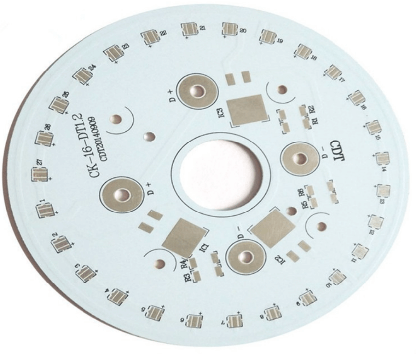
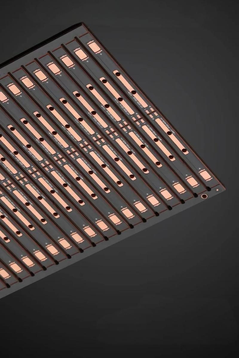
The layout design of an MCPCB involves optimizing the placement of components to ensure even heat distribution. High-power components, such as LEDs or power transistors, are positioned strategically to minimize thermal buildup. Thermal vias may be incorporated to enhance heat transfer through the board.

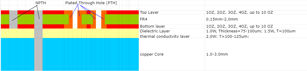
The dielectric layer, which sits between the metal core and the copper circuit layer, must have high thermal conductivity while maintaining electrical insulation. Surface finishes, such as ENIG (Electroless Nickel Immersion Gold) or HASL (Hot Air Solder Leveling), are applied to protect the circuit layer and ensure high solderability.

What are the materials in Mcpcb?

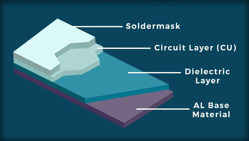
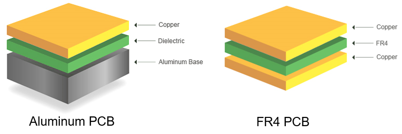
The construction of an MCPCB consists of multiple layers, each serving a specific function. The metal base is typically made from aluminum, copper, or steel, providing a solid foundation for heat dissipation.

MCPCB prototype: What is Metal Core PCB?

Above the metal base lies the dielectric layer, which is a thermally conductive but electrically insulating material that allows heat to pass through while preventing electrical shorts.

The topmost layer is the copper circuit layer, where electrical components are placed. The thickness of this copper layer varies depending on the current-carrying requirements of the circuit. A protective solder mask is applied over the copper traces to prevent oxidation and unintentional short circuits.

Additionally, a silkscreen layer may be added for labeling and component identification. The choice of these materials significantly impacts the board’s thermal conductivity, durability, and overall performance.

What is the thermal conductivity of Mcpcb?

Thermal conductivity is a key property of MCPCBs, as it determines how effectively the board can transfer heat away from components. The dielectric layer, in particular, plays a crucial role in thermal performance. Standard FR4 PCBs have a thermal conductivity of around 0.3–0.5 W/m·K, whereas MCPCBs typically range from 1 to 8 W/m·K, depending on the materials used.

Aluminum-based MCPCBs generally have a thermal conductivity between 1 and 3 W/m·K, while copper-based MCPCBs can reach up to 8 W/m·K, making them ideal for applications requiring maximum heat dissipation.

What is the function of Mcpcb?

MCPCBs serve a crucial function in thermal management and electrical performance. Their primary role is to dissipate heat efficiently, preventing hotspots and ensuring that components operate at safe temperatures. This thermal regulation improves the longevity and reliability of electronic devices, reducing the risk of overheating and failure.

In addition to heat dissipation, MCPCBs provide mechanical strength and stability, making them suitable for rugged environments where vibrations and mechanical stress are concerns.

MCPCB prototype: What is Metal Core PCB?

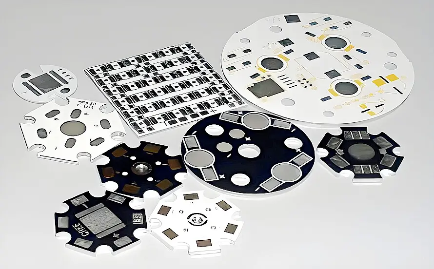
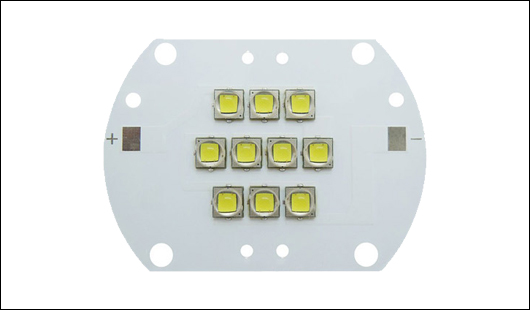
Their ability to handle high power levels makes them ideal for LED lighting, power amplifiers, industrial controls, and automotive electronics.

Unlike traditional PCBs, which struggle with heat-related performance issues, MCPCBs offer a practical solution for high-power applications.

What is the difference between FR4 and Mcpcb?

FR4 and MCPCB differ significantly in terms of thermal performance, material composition, and applications. FR4 PCBs are made from a fiberglass-reinforced epoxy laminate, which provides good electrical insulation but poor thermal conductivity.

However, in high-power electronics, FR4 PCBs struggle to dissipate heat efficiently, leading to performance issues and potential component damage.

MCPCBs, on the other hand, incorporate a metal base that dramatically improves thermal performance. The metal core acts as a heat sink, drawing heat away from components and distributing it across the board. This feature makes MCPCBs ideal for applications where thermal management is critical, such as LED lighting, automotive electronics, and power circuits.

While FR4 PCBs remain popular for general electronics, MCPCBs are the preferred choice for high-power, heat-sensitive applications.

What is the difference between PCB and Mcpcb?

The fundamental difference between standard PCBs and MCPCBs lies in their construction and heat dissipation capabilities. Traditional PCBs use an insulating fiberglass material as their core, whereas MCPCBs use a thermally conductive metal core.

MCPCB prototype: What is Metal Core PCB?

MCPCBs are especially beneficial for industries requiring robust thermal management solutions. In high-brightness LED applications, for example, excessive heat can degrade LED performance and lifespan. MCPCBs prevent this by dissipating heat quickly, ensuring consistent light output and prolonged durability.

Additionally, in power electronics, MCPCBs enable efficient energy conversion and prevent thermal stress, leading to improved performance and reduced failure rates.

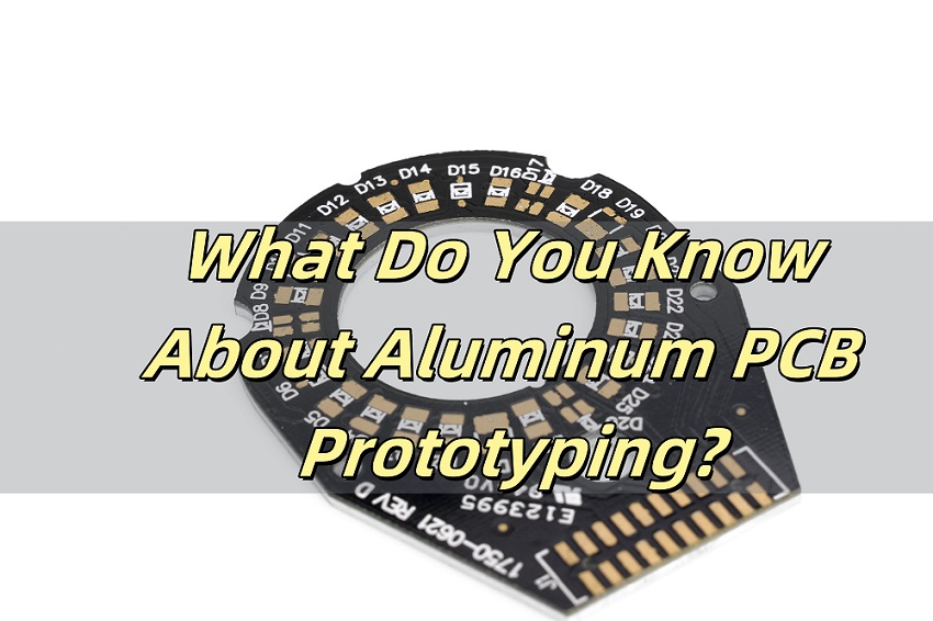
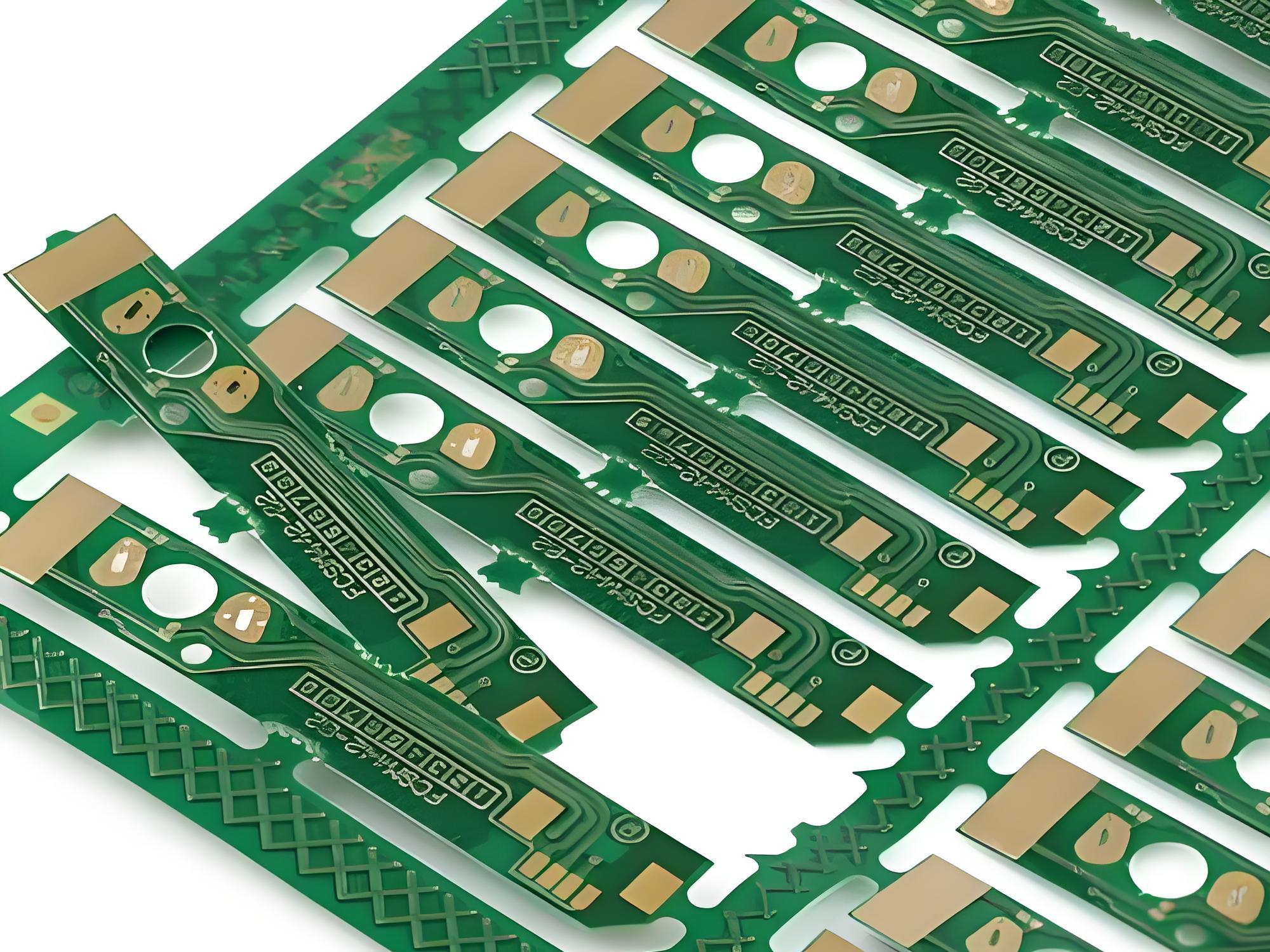
What is a prototype circuit board?

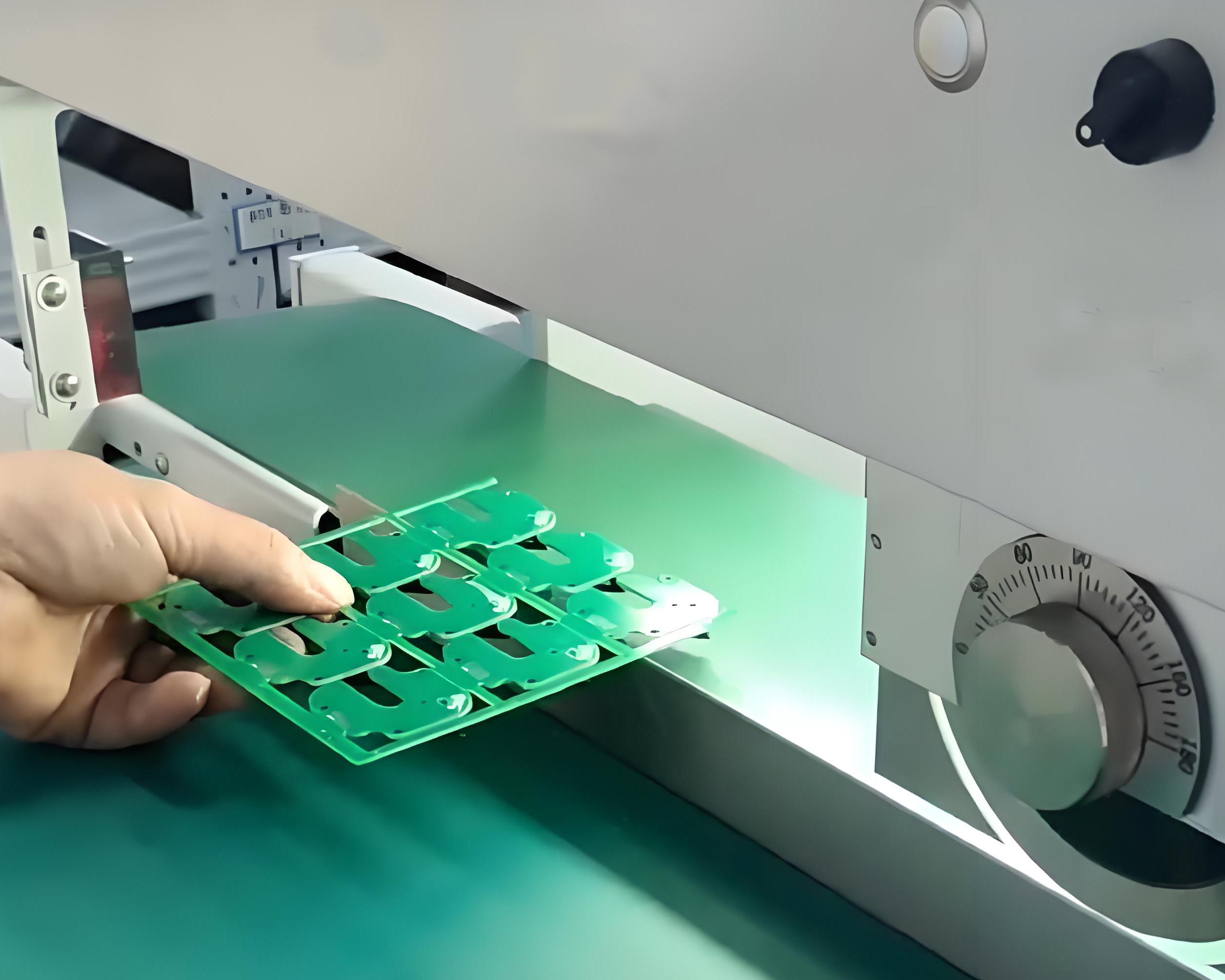
A prototype circuit board is an early-stage version of a PCB used for testing and validation before full-scale production. This process helps reduce production costs and ensures that the final product meets performance requirements.

MCPCB prototypes are particularly valuable in industries that demand high power efficiency and superior thermal management. By testing a prototype, engineers can assess the board’s heat dissipation capabilities, optimize component placement, and make necessary modifications before large-scale manufacturing.

What are the different types of prototype boards?

Prototype boards come in various types, each tailored to specific applications.

Standard FR4 prototype boards are widely used for general circuit testing, offering flexibility and cost-effectiveness.

Flexible PCBs and rigid-flex PCBs are used in compact and wearable devices where space constraints and flexibility are critical.

High-frequency PCBs cater to communication systems requiring stable signal transmission.

MCPCB prototypes stand out for their ability to handle high-power applications with efficient heat dissipation. These prototypes are essential for industries such as automotive, aerospace, and industrial power systems, where thermal management is a top priority.

Conclusion

MCPCBs provide a superior solution for electronic applications requiring effective heat dissipation and durability. Their metal core design enables efficient thermal management, making them the preferred choice for LED lighting, power electronics, and industrial control systems.

For high-quality MCPCB prototyping and manufacturing, EBest Circuit (Best Technology) provides advanced solutions tailored to your specific requirements. Contact us at sales@bestpcbs.com for expert guidance and custom MCPCB solutions.

Copper vs Aluminum Thermal Conductivity: Which transfers heat better?

February 20th, 2025

Copper thermal conductivity plays a significant role in its widespread use across various industries. When it comes to heat transfer, copper is often seen as the go-to material due to its exceptional ability to conduct heat. In this blog, we will explore how copper compares to other metals, especially aluminum, and how its thermal properties impact its performance in different environments. Let’s dive into the world of heat conductivity, from copper’s efficiency to its temperature-dependent behavior.

What Is the Thermal Conductivity of Copper?

Thermal conductivity refers to a material’s ability to conduct heat. Copper stands out as one of the best conductors of heat, making it a popular choice in industries where efficient heat transfer is crucial. The thermal conductivity of copper is approximately 398 W/m·K at room temperature. This high value makes copper the preferred material for various applications, from electrical wiring to heat exchangers.

Interestingly, pure copper offers even higher thermal conductivity compared to alloys, making it an essential material in applications requiring optimal heat management.

What Is the Best Conductor of Heat?

While many metals offer good thermal conductivity, copper is often regarded as the best conductor of heat. Silver, in fact, has a slightly higher thermal conductivity than copper, but due to its cost and scarcity, silver is rarely used in practical applications. Copper’s balance of affordability and efficiency makes it the top choice for industries where heat transfer is critical, such as electronics, automotive, and HVAC systems.

Aluminum, although a good conductor, falls behind copper in terms of efficiency. Copper’s superior performance in both heat conductivity and durability makes it a more reliable material in most heat management scenarios.

What Is the Thermal Conductivity of Copper vs Aluminum?

When comparing the thermal conductivity of copper vs aluminum, copper wins hands down. Aluminum has a thermal conductivity of around 235 W/m·K, which is significantly lower than copper’s. This difference may seem small, but it has a big impact in fields such as electronics and engineering, where heat dissipation is critical.

Copper’s higher conductivity means that it can transfer heat more effectively, making it a better choice for applications that require rapid heat transfer. However, aluminum’s lighter weight and lower cost make it a viable alternative in situations where heat conductivity is not the top priority.

How Does Copper Compare to Other Metals in Thermal Conductivity?

Copper is often compared to metals like aluminum, brass, and nickel. While aluminum is a good conductor, copper far surpasses it in efficiency. On the other hand, brass, which is an alloy of copper and zinc, has lower thermal conductivity than pure copper. Similarly, nickel’s thermal conductivity is also lower than copper’s, which makes copper a preferred material when high heat transfer is needed.

For instance, silver may have the highest thermal conductivity of all metals, but its cost makes it impractical for most applications. Copper strikes a perfect balance, offering excellent heat transfer without the high price tag associated with silver.

How Does Temperature Affect Copper’s Thermal Conductivity?

Copper’s thermal conductivity does not remain constant as temperatures change. As the temperature increases, copper’s thermal conductivity decreases. This is because the atomic vibrations in copper increase with temperature, disrupting the smooth flow of heat.

At room temperature, copper’s conductivity is at its peak. However, as the temperature rises, its ability to conduct heat diminishes. This temperature-dependent behavior must be considered in high-heat applications such as electronics and manufacturing, where managing temperature fluctuations is critical.

At What Temperature Does Copper Melt?

Copper melts at a temperature of 1,984°F (1,085°C). This relatively high melting point is another reason copper is highly favored in industries dealing with extreme temperatures, such as aerospace and power generation. Unlike materials with lower melting points, copper maintains its integrity under heat, providing reliability and durability.

Is Copper or Aluminum Better for Cooling?

When it comes to cooling efficiency, copper generally outperforms aluminum due to its superior thermal conductivity. However, aluminum is often used in cooling applications where weight is a crucial factor, such as in the automotive industry. Copper’s heavier weight might make it less suitable for such purposes, but in situations where heat needs to be transferred quickly and efficiently, copper is the better choice.

In cases like computer processors, where efficient cooling is paramount, copper is often used for heat sinks because of its superior ability to absorb and dissipate heat.

Why Does Copper Have a High Thermal Conductivity?

Copper’s high thermal conductivity can be attributed to its atomic structure. The metal has a highly ordered arrangement of atoms, which allows heat to flow more easily through the material. Additionally, copper’s free electrons move quickly, aiding in the rapid transfer of heat. This ability to efficiently conduct heat is one of the reasons copper is so widely used in heat exchangers, electrical wiring, and other applications where heat dissipation is essential.

In summary, the thermal conductivity of copper makes it the material of choice for a variety of high-performance applications. Whether you’re considering copper vs aluminum thermal conductivity for your projects or exploring how copper compares to other metals like brass or nickel, copper consistently outperforms its competitors in heat transfer efficiency. While aluminum may be lighter and more cost-effective in some situations, copper’s superior thermal properties make it the go-to material in industries where heat management is critical.

At EBest Circuit (Best Technology), we specialize in high-quality PCBs designed for optimal thermal performance. With over 18 years of experience in the industry, we provide solutions tailored to your specific needs. If you’re looking for a reliable partner in heat management, reach out to us at sales@bestpcbs.com for more information or questions.

What Do You Know About Aluminum PCB Prototyping?

January 2nd, 2025

Aluminum PCB prototyping has transformed how electronic designs are tested and refined. It offers a reliable way to create high-performance circuits with enhanced thermal management and durability. Whether you’re developing a small batch for testing or a custom design for specific needs, understanding aluminum PCB prototyping is essential. At EBest Circuit (Best Technology), we specialize in offering tailored aluminum PCB solutions with fast delivery and exceptional quality.

What Is an Aluminum PCB?

An aluminum PCB is a type of printed circuit board with an aluminum core, which acts as a heat sink. This design improves heat dissipation, making it ideal for high-power applications like LED lighting and automotive systems. Its structure includes an aluminum base, an insulating layer, and copper traces. This combination ensures excellent thermal performance and reliability, especially in demanding environments.

What Is PCB Prototyping?

PCB prototyping is the process of creating a preliminary version of a printed circuit board to test its functionality and design. It allows engineers to identify and correct potential flaws before full-scale production. With advancements in technology, prototyping has become faster and more cost-effective, enabling quick iterations for design improvements.

What Is ASIC Prototyping?

ASIC (Application-Specific Integrated Circuit) prototyping involves creating a functional model of a custom-designed chip. While not directly related to PCBs, it shares similarities in testing and refining designs before mass production. Combining ASIC prototyping with aluminum PCB prototyping can optimize performance in high-frequency or power-intensive applications.

How Much Does a PCB Prototype Cost?

The cost of a PCB prototype depends on several factors, including material, complexity, size, and quantity. Aluminum PCB prototypes are generally more expensive than standard FR4 prototypes due to the specialized materials and processes involved. However, their benefits in thermal management and durability often outweigh the higher initial cost. At EBest Circuit (Best Technology), we offer competitive pricing for small and large-scale prototypes, ensuring value without compromising quality.

How to Make PCB Prototyping?

PCB prototyping involves several steps:

Designing the Circuit: Engineers create a detailed schematic using design software.

Fabrication: The design is transferred onto the aluminum base through processes like etching and drilling.

Assembly: Components are soldered onto the board.

Testing: The prototype undergoes rigorous testing to verify performance.

Advanced tools and precise manufacturing are critical to ensuring the prototype matches the design requirements.

How Do You Make a Circuit with Aluminum Foil?

Creating a simple circuit with aluminum foil is a basic DIY project often used for educational purposes. Aluminum foil serves as the conductive path for electricity. While this method is not suitable for professional applications, it demonstrates the principles of electrical circuits. For real-world use, aluminum PCBs provide far superior performance and reliability.

How Do You Make Aluminum PCB?

Manufacturing an aluminum PCB involves:

Material Preparation: Selecting a high-quality aluminum core.

Lamination: Adding an insulating layer and copper foil.

Patterning: Using photolithography to create the circuit pattern.

Etching: Removing excess copper to form the traces.

Drilling and Plating: Creating holes and coating them with conductive material.

Each step requires precision to ensure the PCB meets technical and thermal specifications.

What Are the Advantages of Aluminum PCB?

Aluminum PCBs are known for their thermal conductivity, durability, and environmental friendliness. They effectively dissipate heat, reducing the risk of component failure. Their robust structure ensures longevity, even in harsh conditions. Additionally, aluminum is recyclable, making these PCBs an eco-conscious choice. With these benefits, aluminum PCBs are widely used in LED lighting, automotive systems, and power electronics.

Why Choose EBest Circuit (Best Technology)?

EBest Circuit (Best Technology) stands out for offering a wide range of products, small quantity orders, and high-quality standards. Our expertise in aluminum PCB prototyping ensures fast delivery and fully customized solutions. We prioritize customer satisfaction by delivering exceptional service and reliable results.

In Conclusion, aluminum PCB prototyping bridges the gap between innovative design and practical application. Its ability to combine thermal performance with reliability makes it a top choice for modern electronics. At EBest Circuit (Best Technology), we are dedicated to supporting your prototyping needs with superior quality and customized solutions. Trust us for your next project, and experience the Best in PCB manufacturing.

Aluminum PCB LED, Aluminum Base PCBs for LEDs

December 31st, 2024

An aluminum PCB LED refers to a specialized printed circuit board (PCB) that uses an aluminum base to support and enhance LED (Light Emitting Diode) applications. These PCBs are specifically designed to manage the heat generated by LEDs during operation. In essence, an aluminum PCB LED combines the benefits of advanced circuit design with excellent thermal conductivity, ensuring optimal performance for LED systems.

Aluminum PCBs have revolutionized LED lighting by addressing heat dissipation challenges. These circuit boards, crafted with an aluminum base, deliver excellent thermal management, durability, and efficiency. This blog explores their material composition, thermal properties, and significance in LED applications. Whether you’re designing LED systems or curious about the advantages of aluminum PCBs, this comprehensive guide offers valuable insights.

What Is the LED of Aluminum?

LEDs mounted on aluminum PCBs are essential for applications demanding high efficiency and longevity. The aluminum base acts as a thermal conductor, transferring heat away from the LED components. This process enhances the lifespan and performance of LEDs, particularly in high-power applications like floodlights and automotive lighting. These PCBs are also lightweight, making them suitable for compact designs.

What Is the Material of Aluminum PCB?

Aluminum PCBs typically consist of three layers:

1. Base Layer: Made of aluminum, this layer provides structural support and excellent heat dissipation.

2. Dielectric Layer: Positioned between the base and the circuit layer, it ensures electrical insulation while conducting heat.

3. Circuit Layer: Copper circuits are etched onto this layer to form the electrical connections.

The combination of aluminum and copper enhances conductivity and thermal efficiency. These materials make aluminum PCBs reliable for LED applications.

What Temperature Can Aluminum PCB Withstand?

Aluminum PCBs are designed to operate in high-temperature environments. They can typically withstand temperatures between 120°C and 150°C, depending on the design and material quality. High thermal resistance ensures consistent performance, even in demanding applications like outdoor LED lighting and automotive headlights. Selecting the right PCB thickness and dielectric material is critical for optimizing thermal tolerance.

What Is the Thermal Resistance of Aluminum PCB?

The thermal resistance of an aluminum PCB is the measure of its heat transfer capability. It typically ranges between 1.0°C/W and 2.0°C/W, depending on the board’s structure and material quality. Lower thermal resistance indicates better heat dissipation, which is essential for high-power LEDs. Aluminum PCBs achieve this through their unique combination of metal cores and dielectric materials.

How Thick Is Aluminum PCB?

Aluminum PCBs vary in thickness to suit different applications. Common thicknesses include:

Base Layer: Typically 1.0mm to 2.0mm.

Dielectric Layer: Around 0.075mm to 0.15mm.

Circuit Layer: Common circuit layer thickness is about 0.035mm‌.

The choice of thickness depends on the required mechanical strength, heat dissipation, and electrical load. Thicker boards are ideal for heavy-duty applications like industrial LED lighting.

What Is the Difference Between Copper and Aluminum PCB?

Copper and aluminum PCBs serve similar purposes but have distinct characteristics:

Thermal Conductivity: Copper PCBs offer higher conductivity, while aluminum PCBs balance thermal performance and cost.

Weight: Aluminum PCBs are lighter, making them ideal for compact designs.

Cost: Aluminum PCBs are generally more affordable than copper-based alternatives.

Aluminum PCBs are preferred for LED applications due to their efficient heat dissipation and lower production costs.

How Do You Connect LED to PCB?

Connecting LEDs to aluminum PCBs involves precise soldering. Here’s a simplified process:

1. Prepare the PCB: Clean the board and check the circuit layout.

2. Place the LED: Align the LED pins with the PCB pads.

3. Solder the Connections: Use a soldering iron to secure the LED.

4. Test the Circuit: Verify functionality with a power supply.

Aluminum PCBs are designed to handle heat generated during soldering, ensuring durability and reliable connections.

Why Use Aluminum PCB?

Aluminum PCBs are preferred for LED applications due to several reasons:

1. Heat Management: They efficiently dissipate heat, ensuring LEDs operate at optimal temperatures.

2. Durability: Aluminum provides structural strength and resistance to wear.

3. Lightweight: The boards are easy to integrate into compact devices.

4. Energy Efficiency: They reduce thermal losses, improving overall efficiency.

These features make aluminum PCBs a cornerstone in modern LED lighting solutions, from consumer electronics to industrial systems. EBest Circuit (Best Technology)’s competitive edge lies in its ability to deliver multiple types of products, customized to your needs, with fast delivery and unmatched quality.

What are Applications of Aluminum PCBs in LEDs?

Aluminum PCBs (Printed Circuit Boards) are widely used in LED applications due to their excellent thermal management properties. Here are the main applications of aluminum PCBs in LEDs:

1. High-Power LED Lighting: Aluminum PCBs are ideal for high-power LED lighting systems, such as streetlights, floodlights, and spotlights. The metal core provides effective heat dissipation, preventing LEDs from overheating and improving their efficiency and lifespan.

2. LED Modules for Displays: Aluminum PCBs are used in LED modules for large-scale digital displays, such as billboards and signage. The thermal management capacity of aluminum ensures the stability of the LEDs during continuous operation.

3. Automotive Lighting: In automotive lighting systems, aluminum PCBs are used for headlights, tail lights, and interior lighting. The ability of aluminum to manage heat is critical to maintain LED performance and prevent failure in harsh automotive environments.

4. Backlighting for LCD Displays: Aluminum PCBs are used in the backlight systems of LCD displays, such as those in TVs, monitors, and smartphones. The heat dissipation capabilities enhance the longevity and reliability of the LEDs used for backlighting.

In each of these applications, aluminum PCBs help to reduce the risk of overheating, enhance the performance of LEDs, and extend their operational life, making them a preferred choice for various LED-based lighting and display systems.

In conclusion, aluminum PCBs are indispensable for high-performance LED applications. Their superior thermal management, lightweight construction, and cost-effectiveness provide unparalleled benefits. Choosing the right aluminum PCB for your LED projects ensures durability and efficiency. If you need customized solutions, EBest Circuit (Best Technology) offers premium aluminum PCB led tailored to your requirements. Just feel free to contact us via sales@bestpcbs.com.

Aluminum Core PCB Material, Aluminum PCB Stackup

December 27th, 2024

Aluminum Core PCB Material mainly consists of ‌aluminum, copper foil, and an insulating layer‌. Aluminum PCB Stackup refers to the specific layer structure and arrangement of an aluminum-based printed circuit board (PCB)‌.

The most distinguishing feature of an aluminum PCB is its metal core, which is typically made of aluminum. Above the aluminum core, there is an insulating layer made from a high-performance dielectric material. On top of the dielectric layer, there is a copper layer where the circuit traces are etched. In some cases, there is a final protective coating or layer, such as solder mask or a conformal coating, placed over the copper traces. Whether you’re designing a high-performance device or a simple circuit board, understanding the materials and structure behind aluminum PCBs can help you make the right choice.

What is the material of aluminum PCB?

Aluminum PCBs are made primarily from aluminum, a material known for its excellent thermal conductivity, light weight, and high durability. The core of these PCBs is made of a solid aluminum base, which helps in dissipating heat away from the components. This makes them ideal for applications that involve high power and heat generation, such as power supplies, LED lighting, and automotive electronics.

In addition to the aluminum base, the board also includes a layer of insulating material, usually made from epoxy resin or other high-performance substrates. The insulating layer is key to preventing electrical conductivity between the aluminum and the circuit traces.

What is the material of metal core PCB?

Metal core PCBs, often referred to as MCPCBs, are made from a variety of metal materials, with aluminum being the most common. Other metals, such as copper and iron, can also be used for the core. However, aluminum is favored due to its superior thermal conductivity, cost-effectiveness, and ease of fabrication.

The construction of metal core PCBs generally involves three main layers: the metal base, an insulating dielectric layer, and the copper circuitry. The insulating layer separates the metal core from the copper traces, ensuring that the circuit functions as intended while preventing short circuits.

What is PCB core made of?

The PCB core is typically made from a conductive metal base, which is then covered with a layer of insulating material. For aluminum core PCBs, the core is an aluminum sheet, which is highly effective at conducting heat away from the components mounted on the PCB. The aluminum is often coated with a thin layer of insulation, such as an epoxy resin, which helps protect the metal and ensures that electrical components do not come into direct contact with the aluminum.

In more traditional PCBs, the core is often made of materials like FR4 (a fiberglass-based material), which provides mechanical strength and electrical insulation. However, aluminum core PCBs are preferred in applications where heat management is crucial, as aluminum offers far superior heat dissipation properties.

What material is commonly used for PCBs?

The material commonly used for PCBs varies depending on the application and the specific needs of the circuit. Standard PCBs often use materials such as FR4, a composite material made of fiberglass and epoxy resin. This material is inexpensive and easy to work with, making it the most widely used in everyday electronic devices.

However, in high-performance applications, materials with better thermal conductivity, such as aluminum, are used. These are typically referred to as metal core PCBs or MCPCBs. Aluminum, in particular, is a popular choice because of its combination of excellent thermal management and cost-efficiency.

What is the structure of aluminum PCB?

The structure of an aluminum PCB consists of several layers, each serving a specific purpose. The typical stackup includes:

Aluminum Core: The base layer made of aluminum, which provides heat dissipation.

Dielectric Insulating Layer: A layer of insulating material, typically made from epoxy or other high-performance resins, which electrically isolates the metal from the circuit traces.

Copper Layer: The top layer where the circuit traces are etched. This layer is where the components are mounted, and electrical connections are made.

The aluminum core helps dissipate the heat generated by the components, ensuring that the PCB can handle high-power applications without overheating. The insulating layer prevents short circuits by isolating the copper traces from the aluminum base.

Why use aluminum PCB?

Aluminum PCBs are used primarily for their ability to manage heat effectively. In applications where excessive heat is generated, such as in LED lighting systems or power electronics, aluminum PCBs are essential. The aluminum core helps in quickly transferring heat away from sensitive components, preventing damage and ensuring the device operates efficiently for longer periods.

Another benefit of aluminum PCBs is their lightweight nature, which makes them ideal for applications where weight is a consideration. The low cost of aluminum, compared to other materials like copper, also makes aluminum PCBs a more budget-friendly option without compromising on performance.

Furthermore, aluminum PCBs are extremely durable, offering high resistance to physical wear and corrosion. This makes them a good choice for outdoor or harsh environment applications, such as automotive or industrial equipment.

How do you make Aluminum PCB?

Manufacturing an aluminum PCB involves several steps. Below is a simplified process:

Designing the PCB: The first step is designing the PCB using CAD software. This includes specifying the copper traces, component placement, and thermal management requirements.

Creating the Aluminum Base: The aluminum base is cut and shaped to the required size. It is then coated with a thin layer of insulating material to electrically isolate the aluminum from the circuit traces.

Etching the Copper Layer: The copper layer is then applied to the insulating layer, and the circuit traces are etched into the copper using a photolithography process. This step defines the electrical pathways.

Drilling and Component Mounting: Holes are drilled into the PCB to allow for component placement, and the components are then soldered onto the board.

Testing and Inspection: Once assembled, the PCB undergoes thorough testing to ensure it meets quality standards and functions as intended. This includes thermal testing to check the heat dissipation capabilities of the aluminum core.

Aluminum core PCBs are an excellent choice for applications that require efficient heat dissipation and durability. Their unique structure, consisting of an aluminum base, insulating layer, and copper circuitry, makes them ideal for power-hungry devices like LEDs, power supplies, and automotive electronics. Understanding the materials used in aluminum PCBs and the stackup structure can help you make informed decisions when designing your own boards. When it comes to sourcing aluminum PCBs, choosing the right supplier is critical. EBest Circuit (Best Technology) provides high-quality aluminum core PCBs that meet stringent performance standards and are customizable for your specific needs. Reach out to us at sales@bestpcbs.com for more details.

Aluminum Base PCB: Knowing its Benefits and Applications

December 26th, 2024

Aluminum base PCB (Printed Circuit Board) is an essential part of modern electronics, particularly for applications where heat dissipation is critical. These PCBs are designed to provide effective heat management, which is why they are widely used in high-power LED systems, automotive electronics, and other devices that generate significant heat. In this article, we’ll explore the key features of aluminum base PCBs, including their thermal properties, construction, and benefits compared to other PCB materials.

What is Aluminum PCB?

An aluminum PCB is a type of metal-based PCB that uses an aluminum substrate to provide better thermal conductivity. The aluminum material acts as both a conductor for electrical signals and a heat sink to dissipate heat away from sensitive components. Aluminum PCBs are typically used in high-power applications where managing heat is a crucial concern, such as in LED lighting, power supplies, and automotive electronics.

The design of aluminum base PCBs consists of three layers: the copper layer, the dielectric layer, and the aluminum base. The copper layer carries the electrical signals, while the dielectric layer insulates and binds the copper to the aluminum base. This combination ensures both electrical efficiency and heat management.

What is the Thermal Resistance of Aluminum PCB?  

The thermal resistance of an aluminum PCB refers to how well the PCB can resist heat transfer. In most cases, aluminum PCBs have a low thermal resistance, meaning they efficiently transfer heat away from the components.‌ The thermal resistance of aluminum substrates is usually between 1.0 and 3.2℃/W. Most aluminum substrates have a thermal resistance greater than 1℃/W, while high thermal conductivity aluminum substrates have a thermal resistance less than 0.5℃/W or lower. For example, the thermal resistance of a tin-sprayed aluminum substrate can reach 1.7℃/W or 3.2℃/W.‌ The specific thermal resistance can depend on the thickness of the copper and dielectric layers, but generally, aluminum PCBs are known for their superior heat dissipation properties.

In comparison to traditional FR4 PCBs, aluminum-based PCBs offer much better thermal management, making them a popular choice for power-hungry devices like high-power LEDs. This efficient heat dissipation helps to maintain the stability and performance of the device, preventing overheating and reducing the risk of failure.

What is the Maximum Temperature for Aluminum PCB?

The maximum temperature an aluminum PCB can withstand depends on the design and the materials used. However, most aluminum base PCBs can operate effectively at temperatures ranging from -40°C to 150°C(Even higher, but may be limited in long-term use). Some specialized designs can even handle more higher temperatures.

Aluminum PCBs are often chosen for their ability to operate in high-temperature environments without compromising performance. This makes them an excellent choice for industries like automotive, telecommunications, and lighting, where high temperatures are common.

How Thick is Aluminum PCB?

The thickness of an aluminum PCB can vary depending on its application and the heat dissipation requirements. Typically, the aluminum base layer ranges from 0.8mm to 3.0mm, with thicker layers providing better heat dissipation. The thickness of the copper layer also plays a role, as thicker copper helps to better handle high-power applications.

For instance, a 12w LED aluminum base PCB would typically use a copper thickness of about 1 oz/ftÂČ to 2 oz/ftÂČ, whereas a 25w LED aluminum base PCB would require a thicker copper layer to handle the increased power. Thicker aluminum layers are used in devices that generate significant heat, such as LED drivers and power supplies.

What is the Difference Between FR4 and Aluminum PCB?

The primary difference between FR4 PCBs and aluminum PCBs lies in their substrate material. FR4 is a composite material made of woven fiberglass and epoxy resin, while aluminum PCB uses aluminum as the base layer.

FR4 is widely used for general applications because it is cost-effective and offers good electrical insulation. However, it doesn’t provide the same level of heat dissipation as aluminum PCBs. Aluminum-based PCBs, on the other hand, are specifically designed to manage heat more effectively, which is why they are preferred for high-power applications like aluminum base LED PCBs and metal-based aluminum PCBs.

Another key difference is that aluminum PCBs are generally thicker and more rigid than FR4 boards, offering better mechanical strength. While FR4 is a great choice for lower-power devices, aluminum PCBs are the go-to solution for heat-intensive applications. EBest Circuit (Best Technology) stands out by providing customized, high-quality products with quick turnaround times, all backed by our top-tier customer service.

What is the Best PCB Material for Heat Dissipation?

Aluminum is the best material for heat dissipation when it comes to PCBs. Aluminum base PCBs excel in transferring heat away from sensitive components, ensuring that devices do not overheat during operation. Other materials like copper and ceramic also have good thermal properties, but aluminum provides a balanced combination of cost, performance, and manufacturability.

For high-power devices like LED aluminum base PCBs or metal-based aluminum PCB boards, aluminum is the material of choice due to its excellent thermal conductivity, which helps maintain the optimal performance and longevity of the device.

How Do Aluminum PCBs Work?

Aluminum PCBs work by using the aluminum base to conduct heat away from the components mounted on the board. When an electronic component, such as an LED, operates, it generates heat. In a traditional PCB made from materials like FR4, this heat can build up, causing the components to overheat and potentially fail.

With aluminum PCBs, the heat generated by the components is quickly transferred through the copper and dielectric layers to the aluminum base. From there, the heat is dissipated into the surrounding environment, preventing overheating. This process ensures that the components remain within their safe operating temperature range, thus improving the reliability and lifespan of the device.

For example, aluminum-based LED PCBs are specifically designed to handle the high heat generated by LEDs, keeping them cool and allowing them to operate efficiently without degradation.

Aluminum base PCBs offer superior thermal management, making them ideal for high-power applications that require efficient heat dissipation. From aluminum base LED PCBs to metal-based aluminum PCB boards, these PCBs help prevent overheating, increase reliability, and improve the overall performance of electronic devices. Whether you are designing a 25w PCB LED aluminum star base or a single layer LED aluminum base PCB, aluminum offers excellent heat resistance and thermal conductivity.

When selecting the right PCB material, aluminum base PCBs should be at the top of your list for any application where heat management is a priority. With their ability to handle high temperatures and provide better mechanical strength than traditional materials like FR4, aluminum-based PCBs are the best choice for applications such as LED lighting, power supplies, and other high-power electronics.

Choose aluminum base PCBs for your next project and experience improved performance, longer lifespan, and efficient heat management. EBest Circuit (Best Technology) offers a wide range of aluminum base pcb products with high quality, tailored to meet the specific needs of each customer. Pls feel free to reach out to us at sales@bestpcbs.com for more details.

What are PCB Designs Called?

November 29th, 2024

If you’re working with electronics, you’ve probably heard of Printed Circuit Boards (PCBs). They’re at the heart of almost every electronic device we use today. But have you ever wondered what are PCB designs called? Are they just called PCB designs, or is there more to it? Well, it turns out there are quite a few terms for PCB designs, and each one refers to a specific aspect of the design process. Let’s take a closer look at these terms, how they’re used, and what makes each one unique.

What are PCB Designs Called?

What Are PCB Designs Called?

PCB designs are often referred to by different names depending on the context or the stage of the design process. Let’s explore the most common terms:

1. PCB Layout

This is probably the most frequently used term. When someone mentions a PCB layout, they’re talking about the physical arrangement of components and the routing of electrical connections (also called traces) on the board.

Think of it like designing the floor plan of a house. The layout ensures that everything fits within the available space and that all the rooms (or in this case, components) are connected in the right way.

What are PCB Designs Called?

2. Circuit Board Design

Sometimes, you’ll hear people refer to the process as circuit board design. This term emphasizes the broader design aspect, from planning the circuit to placing components and routing connections. It’s a more general term that covers everything from the initial schematic to the final layout.

3. PCB Schematic

While the schematic is technically just one part of the design process, some people refer to the entire design as the schematic. This is more common among those who focus on the circuit’s logic rather than its physical structure.

4. Gerber Files

Once the design is complete, it’s converted into a set of files called Gerber files. These files contain all the information needed to manufacture the PCB. Sometimes, people use the term Gerber files to refer to the finished design, even though it’s technically just the output.

5. EDA (Electronic Design Automation) File

In professional environments, PCB designs are often called EDA files. These are the files created by design software like Altium Designer, KiCad, or Eagle. They contain all the details of the design, including the schematic, layout, and design rules.

What Is the Difference Between a PCB Design and a Schematic Design?

Many people use the terms PCB design and schematic design interchangeably, but they serve different purposes in the design process.

Schematic Design

  • Represents the electrical connections between components.
  • Focuses on the logic and functionality of the circuit.
  • Uses symbols to represent components like resistors, capacitors, and transistors.
  • Helps engineers understand how the circuit works.

PCB Design

  • Translates the schematic into a physical layout.
  • Focuses on the placement of components and routing of traces.
  • Considers factors like board size, layer count, and thermal performance.
  • Ensures the circuit can be manufactured and assembled.

In summary, the schematic shows what the circuit does, while the PCB design shows how it does it physically.

PCB Schematics Elements

A schematic is the starting point for any PCB design. It provides a clear visual representation of the circuit’s functionality. Here are the key elements of a schematic:

What are PCB Designs Called?

1. Component Symbols

Each component in the circuit is represented by a symbol. For example, a resistor is usually shown as a zigzag line, while a capacitor is two parallel lines.

2. Nets (Connections)

Lines connecting the symbols represent electrical connections, known as nets. These nets define how components interact with each other.

3. Reference Designators

Lines connecting the symbols represent electrical connections, known as nets. These nets define how components interact with each other.

4. Values and Ratings

The schematic also shows the values and ratings of components, such as the resistance of a resistor or the capacitance of a capacitor.

5. Power and Ground Symbols

Every circuit needs power and ground connections. These are represented by standard symbols, ensuring the circuit has a common reference point for voltage.

Common Terms in PCB Design

1. Silkscreen Layer

The silkscreen layer contains text, logos, and symbols printed on the surface of the PCB to help identify components and guide assembly. It can also include part numbers, component values, and polarity markings.

2. Via

A via is a hole in the PCB that allows electrical connections between different layers. Vias are often used in multi-layer PCBs to route signals between the top and bottom layers or inner layers.

3. Copper Pour

A copper pour is a large, solid region of copper that is poured over areas like ground or power planes. It helps reduce noise, increase current-carrying capacity, and improve thermal dissipation.

4. Trace Width

Trace width refers to the thickness of the copper traces used to connect components. The width of a trace must be designed to carry the required amount of current without overheating.

5. Drill Hole

A drill hole is a hole that is made in the PCB to accommodate components with leads or for vias. The size and placement of drill holes are critical to the assembly process.

6. Solder Mask

The solder mask is a protective layer applied over the PCB to prevent solder from bridging between pads. It also helps prevent oxidation of the copper traces and improves the board’s overall durability.

7. Pad

Pads are small copper areas on the PCB where components are mounted or soldered. Pads can be through-hole or surface-mount, depending on the type of component.

8. Bill of Materials (BOM)

The BOM is a comprehensive list of all the components required for the assembly of a PCB. It includes details like part numbers, quantities, and specifications for each component.

9. Impedance Control

Impedance control is the process of ensuring that the impedance of the PCB traces matches the requirements of the signals that will travel through them. This is important for high-speed and RF circuits.

10. Stack-up

Stack-up refers to the arrangement of layers in a multi-layer PCB. It defines how the copper, dielectric, and other materials are stacked to create the board.

11. Daisy-Chaining

Daisy-chaining is a method of connecting multiple components or pins in a series, often used in signal or power distribution systems within the PCB design.

12. Overcurrent Protection

Overcurrent protection refers to circuits designed to prevent excessive current from flowing through the PCB traces, often by using fuses or resistors that limit the current flow.

13. Design for Manufacturability (DFM)

DFM refers to designing the PCB in a way that makes it easier and more cost-effective to manufacture. This includes factors like trace width, pad size, and component placement.

14. Routing

Routing is the process of designing the electrical paths that connect the components on a PCB. Proper routing ensures that signals are carried efficiently with minimal interference.

15. Thermal Via

Thermal vias are specially designed vias used to transfer heat away from high-heat components to other parts of the PCB or a heat sink.

16. Electromagnetic Interference (EMI) Shielding

EMI shielding involves using design techniques, such as grounding and the use of shielding components, to protect sensitive parts of the PCB from electromagnetic interference.

17. Differential Pair

A differential pair is a set of two traces that carry complementary signals, often used in high-speed designs like USB or Ethernet to minimize noise and improve signal integrity.

18. Power Distribution Network (PDN)

The PDN refers to the system of traces and planes that deliver power to various components on the PCB. Proper PDN design is crucial to ensure reliable power delivery and minimize voltage drops.

19. Electrical Rule Check (ERC)

ERC is a process that checks the schematic design for electrical issues like unconnected nets, incorrect component connections, or incorrect power supply connections.

20. Multi-layer PCB

A multi-layer PCB contains more than two layers of conductive material and is used for more complex designs that require high-density circuits, especially in smaller devices.

21. Surface-Mount Technology (SMT)

SMT is a method for mounting components directly onto the surface of the PCB, rather than inserting them through holes. This allows for smaller, more compact designs.

22. Through-Hole Technology

Through-hole technology involves inserting component leads through holes in the PCB and soldering them on the opposite side. It’s commonly used for components that require strong mechanical bonds.

23. Hot Air Soldering

A method of soldering components onto the PCB using hot air, often used in reflow soldering processes for surface-mount components.

24. Trace Routing

Trace routing is the process of laying out the paths that the electrical signals will take through the PCB. Good trace routing ensures efficient and reliable signal transmission.

25. Tenting

Tenting refers to the process of covering the vias with a layer of solder mask, leaving the pad open. It helps prevent solder from flowing into vias during soldering.

PCB Design vs. PCB Layout

Although often used interchangeably, PCB design and PCB layout have different meanings:

PCB Design: Refers to the entire process, from schematic creation to generating manufacturing files.

PCB Layout: Specifically focuses on the physical arrangement of components and routing of traces on the board.

In simple terms, PCB layout is a part of the overall PCB design process.

PCB Design Process

Designing a PCB is a multi-step process that requires careful planning and attention to detail.

1. Schematic Capture

The process starts with creating a schematic diagram that defines the circuit’s functionality and connections.

2. Component Selection

Next, components are selected based on the circuit requirements. Factors like size, power rating, and cost are considered.

3. PCB Layout

Components are placed on the board, and traces are routed to connect them. This step requires balancing electrical performance with physical constraints.

4. Design Rules Check (DRC)

The layout is checked for errors or violations of design rules to ensure it meets manufacturing standards.

5. Gerber File Generation

Once the design is complete, Gerber files are generated. These files are used by manufacturers to produce the PCB.

6. Fabrication and Assembly

The PCB is fabricated, and components are assembled to create the final product.

FAQs

Q: What software is used for PCB design?

A: Popular software includes Altium Designer, Eagle, KiCad, and OrCAD.

Q: How many layers can a PCB have?

A: PCBs can have anywhere from one to 16 or more layers, depending on complexity.

Q: Why is trace width important?

A: Trace width affects the current-carrying capacity and signal integrity of the circuit.

Q: What is a multilayer PCB?

A: A multilayer PCB has multiple layers of copper separated by insulating material, allowing for more complex designs.

Q: How long does it take to design a PCB?

A: The time varies based on complexity. Simple designs may take a few days, while complex designs can take weeks.

Can I design microvias in multilayer MCPCB?

October 12th, 2024

What is a Microvias?

A microvia is a small hole drilled into a PCB that connects different layers. They are essential for high-density interconnections and are commonly used in advanced electronic designs. Typically, microvias equal to or less than 150 microns drilled on the PCB board with a laser. In 2013, the IPC standard changed the definition of microvias to those with an aspect ratio of 1:1. Ratio of aperture to depth (not exceeding 0.25mm). Previously, micropores were less than or equal to 0.15 mm in diameter, so they typically spanned only one layer.

Can I design microvias in multilayer MCPCB?

Because the diameter is very small compared to mechanically drilled through holes (PTH), we define them as microvias, usually connecting only one layer of the board to its adjacent layers. These through holes reduce the possibility of any type of manufacturing defect because they are laser drilled, thus reducing the possibility of any residue remaining after the process. Because of their small size and ability to connect one layer to the next, they can make dense printed circuit boards with more complex designs.

Types of Microvias

There are two types of microvias in the PCB design – stacked microvias and staggered microvias.

  • Stacked Microvias

Stacked microvias are formed by stacking multiple layers on top of each other to provide a path through which current flows. Create a hole in one layer and drill into another layer below. The top layer is welded or welded to the bottom layer to form an interconnect between the two layers. This allows for fast, efficient routing without compromising performance or reliability.

Can I design microvias in multilayer MCPCB?
  • Staggered Microvias

The interlaced microvias is aligned with the pad of the same layer, but is offset from its center by half of the pad diameter. The distance from its center to the edge of the board is also half the diameter of the pad. Staggered microvias allow you to place two through holes in a single pad without overlapping them or having to route wires on different layers together in this location. This type of microvias can be used for electrical connections to the surrounding brass pads and traces.

Can I design microvias in multilayer MCPCB?

What is the Difference Between Vias and Microvias?

Vias and microvias serve similar purposes in connecting different layers of a PCB, but they differ significantly in size and application.

1. Size

One of the most significant differences between vias and microvias is their size. Standard vias typically have a diameter greater than 150 micrometers (ÎŒm), while microvias are defined as having a diameter of 150 ÎŒm or less.

2. Design Complexity

As technology advances, the demand for higher circuit densities and more complex designs has grown. Microvias enable designers to create intricate multilayer circuits that were not possible with standard vias.

3. Layer Connection

Standard vias can connect any number of layers in a PCB, typically running from the outer layer through to the inner layers. In contrast, microvias are usually used for connecting one or two layers. Microvias are commonly employed in multilayer PCBs, where they can connect the outer layer to one or more inner layers without passing through the entire board.

4. Aspect Ratio

The aspect ratio, which is the ratio of the depth of a via to its diameter, is another important difference. Standard vias generally have lower aspect ratios, making them easier to fabricate. Microvias, due to their smaller size, often have higher aspect ratios. A typical aspect ratio for microvias ranges from 1:1 to 2:1.

5. Applications

Standard vias are commonly used in traditional PCB designs for applications where space is not as critical. They are suitable for general-purpose circuits, power distribution, and less complex layouts. In contrast, microvias are essential in high-density applications, such as smartphones, tablets, and advanced computing devices, where compact designs are necessary.

Microvias vs. Blind Via

Blind vias connect the outer layer of the PCB to one or more inner layers without penetrating the entire board. As the name suggests, these through-holes are “blind holes” because they are not visible from the other side of the PCB. Blind holes have several advantages, such as saving space on the board, enabling a more compact design, and improving signal integrity by reducing the length of the signal path.

The blind via passes through the surface layer of the PCB, extending through only a portion of the board to connect the surface layer to one or more inner layers. They are a key component in current PCB designs, allowing surface components to connect to inner layers while minimizing the number of layers required for wiring. The advantages of using blind vias including:

  • Increased density
  • Reduce the number of layers
  • Improved signal performance
  • Good for heat dissipation
  • Improve mechanical strength

Can Microvias be Designed in Multilayer MCPCB?

Yes, microvias can indeed be designed in multilayer MCPCBs. In fact, their small size and efficient design make them ideal for these types of boards. Multilayer MCPCBs often require compact interconnections to accommodate various functionalities, and microvias facilitate this need. By enabling multiple layers to connect efficiently, microvias enhance the overall performance of the MCPCB. Additionally, they contribute to improved thermal management, a critical factor in high-power applications. Their integration in multilayer designs is a significant advantage for modern electronics.

The process for using microvias in multilayer metal-based circuit boards includes the following key steps:

1. Inner laser drilling and plating: This is the first step in the production of microvias, precisely drilled by laser technology, and electroplated.

2. Resin filled: The micro-vias after electroplating are filled with resin to enhance the stability of the structure.

3. Resin grinding: Grind the orifice after the jack hole to ensure a smooth surface.

4. Electroplating: Metallize the surface of the orifice resin to achieve electrical interconnection between layers.

5. Inner circuit etching and outer layer lamination: To complete the production of the inner circuit, and the outer layer of laser drilling and graphic plating, and finally realize the production of multi-layer circuit board.

MCPCB Material in EBest Circuit (Best Technology)

Can I design microvias in multilayer MCPCB?

MCPCB Prototype Lead Time (Vary Depends on the MCPCB Design)

Can I design microvias in multilayer MCPCB?

What is aluminum pcb depaneling?

October 11th, 2024

In the electronic manufacturing process, it is usually necessary to divide a large area of ​​aluminum-based PCB into multiple small pieces so that they can be installed in different electronic devices. Different electronic devices have different requirements for the size of PCBs. Through depaneling, large-area aluminum-based PCBs can be cut into sizes suitable for specific electronic devices.

What is the meaning of depaneling?

Aluminum PCB depaneling refers to cutting multiple circuit boards arranged in a row from a large board into separate small boards. This process is to divide a large aluminum printed circuit board (PCB) into multiple independent and fully functional circuit boards for subsequent assembly and use.

What is aluminum pcb depaneling?

Aluminum PCB depaneling is an important link in the production process of electronic devices, which can improve production efficiency and circuit board flexibility.

What are the methods of PCB depaneling?

There are many ways to depanel aluminum PCBs. Common depaneling methods include:

  • 1. ‌V-cut depaneling‌: Use a V-shaped blade to cut a V-shaped groove on the PCB board, and then separate the aluminum PCB along the groove by external force. This method is suitable for smaller aluminum PCB boards and fine dividing lines.
  • 2. ‌Sawtooth depaneling‌: Cut the aluminum PCB board with a sawtooth cutting tool to form multiple small panels, and then separate the panels by pressure or vibration. This method is suitable for aluminum PCB boards with larger areas.
What is aluminum pcb depaneling?
  • 3. ‌Laser depaneling‌: Use a high-energy-density laser beam to accurately cut the aluminum PCB, which is suitable for production environments with high precision requirements and high efficiency.
  • 4. ‌Chemical corrosion depaneling‌: Corrode the aluminum PCB with a chemical corrosive agent to form a dividing line, and then separate the panels by physical methods.

What is the process of depaneling PCB?

The aluminum PCB depaneling process varies depending on the depaneling method. The common aluminum PCB depaneling methods and processes are as follows:

Manual depaneling

  • Preparation: Check whether the aluminum PCB board meets the conditions for manual depaneling, such as confirming that there are no stress-sensitive components such as SMD (Surface Mounted Devices) on the board, and prepare suitable fixtures and operating space.
  • Positioning and fixing: Place the aluminum PCB concatenated or assembled boards that need to be separated on a stable workbench and fix them with fixtures to ensure that the boards do not move during the separation process. For aluminum PCB boards with V-grooves, align the V-grooves with the direction that is convenient for force application, and ensure that the board is placed in the correct direction and position to facilitate the separation operation.
  • Separation operation: The operator uses both hands or simple tools (such as tweezers, etc., and small cutting tools may be used in some special cases, but they must be operated with caution to avoid damaging the board) along the V-groove to break or separate the aluminum PCB board into individual small boards with appropriate force. During the operation, pay attention to controlling the force and direction to avoid damage to the board due to uneven force or wrong direction.
What is aluminum pcb depaneling?

V-cut board separation machine separation

  • Equipment debugging: Turn on the power of the V-cut board separation machine, and adjust the upper guide knife position and lower knife height of the board separation machine according to the thickness of the aluminum PCB board, the depth and width of the V-groove and other parameters to ensure that the spacing between the upper and lower knives is appropriate and the aluminum PCB board can be accurately cut.
  • Upper board positioning: carefully place the aluminum PCB board with V groove on the workbench of the V-cut board splitter, ensure that the V groove of the aluminum PCB board fits tightly with the lower knife of the board splitter, and the position of the board is accurate to avoid deviation during the cutting process.
  • Board splitting operation: start the V-cut board splitter manually, electrically or pneumatically, so that the blade cuts along the V groove of the aluminum PCB board. During the cutting process, pay attention to the cutting situation to ensure that the cutting depth is moderate and will not cause over-cutting or incomplete cutting of the aluminum PCB board.

What is the manufacturing process of aluminum PCB?

The manufacturing process of aluminum substrate PCB mainly includes the following steps: cutting, drilling, dry and wet film imaging, etching, surface treatment and final inspection. ‌

  • 1. Cutting: Cut the large-sized incoming materials into the size required for production, pay attention to the protection of the aluminum and copper surfaces, and avoid scratches and board edge delamination.
  • 2. Drilling: Position the holes in the board to ensure the correct number and size, and avoid scratches on the board and deviation of the hole position.
  • 3. Wet and dry film imaging: Present the parts required for making the circuit on the board, and pay attention to whether the circuit is open and whether the alignment is deviated after development.
  • 4. Etching: Remove the uncovered parts to form the circuit pattern, and pay attention to the quality and stability of the circuit after etching.
  • 5. Surface treatment: Perform necessary surface treatment on the circuit board, such as tin spraying, to improve the performance and appearance of the circuit board.
  • 6. Final inspection: Perform a final inspection on the completed circuit board to ensure that the quality meets the requirements.

What are the advantages of aluminum PCB?

The main advantages of aluminum substrate PCB include:

  • Excellent heat dissipation performance: The aluminum substrate uses high thermal conductivity aluminum alloy as the core material, which can quickly conduct and dissipate heat, thereby effectively reducing the operating temperature of components.
  • ‌Lightweight design‌: Compared with traditional FR4 substrates, aluminum substrates have lighter weight, which is particularly important in weight-sensitive fields such as aerospace and automobiles, helping to reduce the weight of the overall equipment and improve energy efficiency and operating performance‌.
What is aluminum pcb depaneling?
  • ‌Good mechanical properties‌: Aluminum substrates have high strength and hardness, providing good support and protection for electronic components. At the same time, its excellent impact resistance and vibration resistance enable it to adapt to various complex working environments and ensure the stable operation of the equipment‌.
  • ‌Excellent electrical performance‌: Aluminum substrates have excellent insulation and voltage resistance, which can meet the electrical requirements of electronic equipment in various working environments and provide stable electrical support for the equipment‌.
  • ‌Environmental protection‌: Aluminum substrates are made of environmentally friendly materials, there is no pollution in the production process, and waste is easy to recycle and dispose, which is fully in line with the current trend of green environmental protection‌.
  • ‌Diverse application forms‌: There are many types of aluminum substrates, including flexible aluminum substrates, hybrid aluminum substrates, multi-layer aluminum substrates, etc., suitable for different application needs.

What are the disadvantages of aluminum PCB?

The main disadvantages of aluminum PCB include high cost, difficult process, electrical strength and withstand voltage problems, mismatched thermal conductivity test, inconsistent material specifications, and more defective products. ‌

First, the price of aluminum PCB is relatively high, usually accounting for more than 30% of the product price. This is because the production of aluminum PCB requires the use of high-purity aluminum materials and special processing technology, all of which push up the cost. ‌

Second, the process of aluminum PCB is difficult, especially when it is made into a double-sided board, the process complexity is higher, and it is easy to have problems in electrical strength and withstand voltage. In addition, the mismatch of thermal conductivity test methods and results of aluminum PCB is also a problem. ‌

In addition, the material specifications of aluminum PCB have not yet been unified, and there are multiple standards such as CPCA industry standards, national standards, and international standards, which brings certain uncertainties to production and application. ‌

Why is aluminum no longer used in integrated circuits?

The main reason why aluminum is no longer used in integrated circuits is that copper has replaced aluminum as an interconnect metal material. Copper has lower resistivity and better anti-electromigration performance than aluminum, which makes copper more reliable and effective in high-speed integrated circuits. ‌

Specifically, aluminum may experience electromigration under long-term current, that is, aluminum atoms migrate inside the wire, causing the wire to break or form voids, which in turn causes the integrated circuit to fail. In addition, as the interconnection spacing decreases, the resistance of the aluminum wire increases and the capacitance between the wires increases, resulting in increased RC delay, which is not conducive to high-speed integrated circuits.

Copper has a lower resistivity than aluminum, can transmit current more efficiently, and can carry more current in thinner metal wires. Copper also has higher electromigration resistance than aluminum, making copper interconnects more reliable under high current conditions. These advantages make copper a preferred material for advanced integrated circuit technology.

Aluminum-based PCB depaneling is an important link in the electronic manufacturing process, which directly affects the quality and performance of electronic equipment. By selecting the appropriate depaneling method, controlling the depaneling accuracy, and avoiding damage to the PCB, the quality and efficiency of aluminum-based PCB depaneling can be effectively improved.

2 Layer Aluminum PCB | Metal Core PCB Manufacturer

October 9th, 2024

What is a 2 Layer Aluminum PCB?

A 2-layer aluminum PCB is a type of metal core circuit board that contains two conductive layers, usually copper, with an aluminum core or base material. Aluminum PCBs are used for their excellent heat dissipation properties, and always used in high-power applications like LED lighting, power supplies, and automotive systems. The aluminum base offers better thermal management than standard FR4 PCBs. In a 2-layer aluminum PCB, the two conductive copper layers allow more complex routing for electrical signals compared to single-layer boards.

2 Layer Aluminum PCB | Metal Core PCB Manufacturer

2 Layer Aluminum PCB Stack-Up

The stack-up of a 2-layer aluminum PCB consists of the following:

  • Top Copper Layer: This is where the signal traces and components are located. It can vary in thickness, depending on current-carrying requirements.
  • Dielectric Layer: A layer of insulation that separates the top copper layer from the aluminum core. It plays a key role in electrical isolation and heat transfer.
  • Aluminum Base: This core provides structural support and excellent heat dissipation properties. It also serves as the grounding plane in some designs.
  • Bottom Copper Layer: The second conductive layer allows for more advanced routing.
2 Layer Aluminum PCB | Metal Core PCB Manufacturer

How Thick is a 2 Layer PCB Layer?

The thickness of a 2-layer aluminum PCB can vary depending on the specific design requirements, but typically, the copper layer is about 1 to 2 ounces (35 to 70 microns) thick. The aluminum base itself is thicker, usually between 1.0 mm and 3.0 mm, depending on the board’s required rigidity and heat dissipation needs. The overall board thickness generally ranges between 1.2 mm and 3.2 mm.

A thicker aluminum core improves heat transfer, but the board’s thickness must also align with the product’s mechanical and electrical requirements. Designers often have to balance between sufficient thermal performance and the overall board size for practical applications.

Is Thicker Aluminum PCB have Better Heat Dissipation?

Generally speaking, the thinner the thickness of the aluminum PCB, the faster the heat conduction speed. The thicker the thickness of the aluminum PCB, the slower the heat conduction rate. The thermal conductivity of aluminum-based circuit board mainly depends on its material and structure. Although thickness affects the path length of heat conduction, the more critical factors are the thermal conductivity and structural design of the material. For example, high thermal conductivity materials such as copper, silver and other high thermal conductivity materials will significantly improve the thermal conductivity of aluminum substrate. In addition, the thickness and thermal conductivity of the insulation layer will also affect the overall thermal conductivity effect ‌.

Specifically, the thermal conductivity of the aluminum-based circuit board is also related to the thickness of its insulation layer. The thicker the insulation layer, although it can withstand higher voltage, it will also reduce the heat transfer efficiency. Therefore, choosing the appropriate insulation layer thickness and materials with high thermal conductivity is the key to ensuring efficient thermal conductivity of aluminum-based circuit boards ‌.

2 Layers Aluminum PCB vs. Double Sided Aluminum PCB

Though the terms “2 layers aluminum PCB” and “double-sided aluminum PCB” might sound similar, there are slight differences.

A 2-layer aluminum PCB contains two conductive copper layers. These layers can be arranged to handle signal routing and ground planes separately. In contrast, a double-sided aluminum PCB typically has one copper layer on either side of the aluminum core, offering less flexibility in routing. Here is the stack up of double sided aluminum PCB:

2 Layer Aluminum PCB | Metal Core PCB Manufacturer

How Much Does Aluminum PCB Cost?

The cost of an aluminum PCB, including a 2-layer version, depends on several factors such as the board’s thickness, copper weight, design complexity, and production volume. On average, 2-layer aluminum PCBs cost more than single-sided aluminum PCBs because of the additional copper layer and routing complexity.

For small orders, prices might range between $5 and $15 per square foot. For larger production runs, costs can decrease significantly due to economies of scale. Factors like the thickness of the aluminum base and copper layer, as well as additional features like surface finishes, can also influence the price.

While aluminum PCBs are more expensive than standard FR4 boards, their enhanced thermal performance can reduce overall system costs by improving reliability and reducing the need for additional cooling measures.

How Many Layers Should a PCB Have?

The number of layers a PCB should have depends on the complexity of the design. For simple applications like LED lighting or power conversion, a 2-layer aluminum PCB is often sufficient. It provides more routing flexibility than a single-layer board while still offering effective heat dissipation.

For more complex designs requiring high-density interconnections or additional functionality, a multi-layer PCB with three or more layers might be necessary. However, multi-layer aluminum PCBs are rare because their primary function is thermal management, which is typically solved within one or two layers. The decision to use more layers depends on the specific application, power requirements, and signal integrity needed in the design.

Aluminum PCB Design Guidelines

When designing a 2-layer aluminum PCB, several factors must be considered to maximize performance:

  • Thermal Management: Since aluminum PCBs are chosen for their thermal properties, optimizing heat dissipation is critical. Components that generate significant heat should be placed near the aluminum core, allowing for faster heat transfer.
  • Copper Thickness: The copper thickness should match the current-carrying requirements of the design. Using thicker copper can help manage higher current loads, but it also increases the cost and weight of the PCB.
  • Dielectric Layer: The thickness and material of the dielectric layer play a crucial role in both thermal and electrical performance. A thinner dielectric layer improves heat dissipation but may limit electrical isolation. Choosing the right dielectric material is key for balancing performance and reliability.
  • Via Placement: For a 2-layer design, vias must be carefully placed to connect the two copper layers. Vias should be positioned to minimize electrical interference and maintain signal integrity.
  • Component Placement: Heat-sensitive components should be placed away from high-power components. This minimizes thermal stress on sensitive devices and ensures reliable operation over the PCB’s lifespan.

Aluminum PCBs may come with a higher price tag compared to traditional FR4 boards, but the long-term benefits in heat management, performance, and durability make them an excellent investment for demanding applications. Whether you’re working on power electronics, automotive circuits, or lighting solutions, a 2-layer aluminum PCB can provide the right balance between complexity and thermal efficiency.

If you’re in need of high-quality, custom aluminum PCBs, EBest Circuit (Best Technology) specializes in delivering tailored solutions for your specific design needs. With 18+ years of experience in PCB manufacturing, we ensure top-notch performance, quality, and reliability for all your projects. Let us help you bring your ideas to life with the right aluminum PCB solution!