An RF PCB manufacturer specializes in the design and fabrication of printed circuit boards used in radio-frequency, microwave, and high-frequency electronic systems. As operating frequencies increase, PCB performance is no longer determined only by connectivity, but by electromagnetic behavior, material stability, and manufacturing precision.
This pillar page provides a comprehensive, engineering-focused overview of RF PCB manufacturing. It covers what an RF PCB manufacturer does, how RF PCBs differ from standard boards, RF frequency definitions, materials, stackup design, manufacturing processes, common mistakes, and how to evaluate RF PCB manufacturing capability.
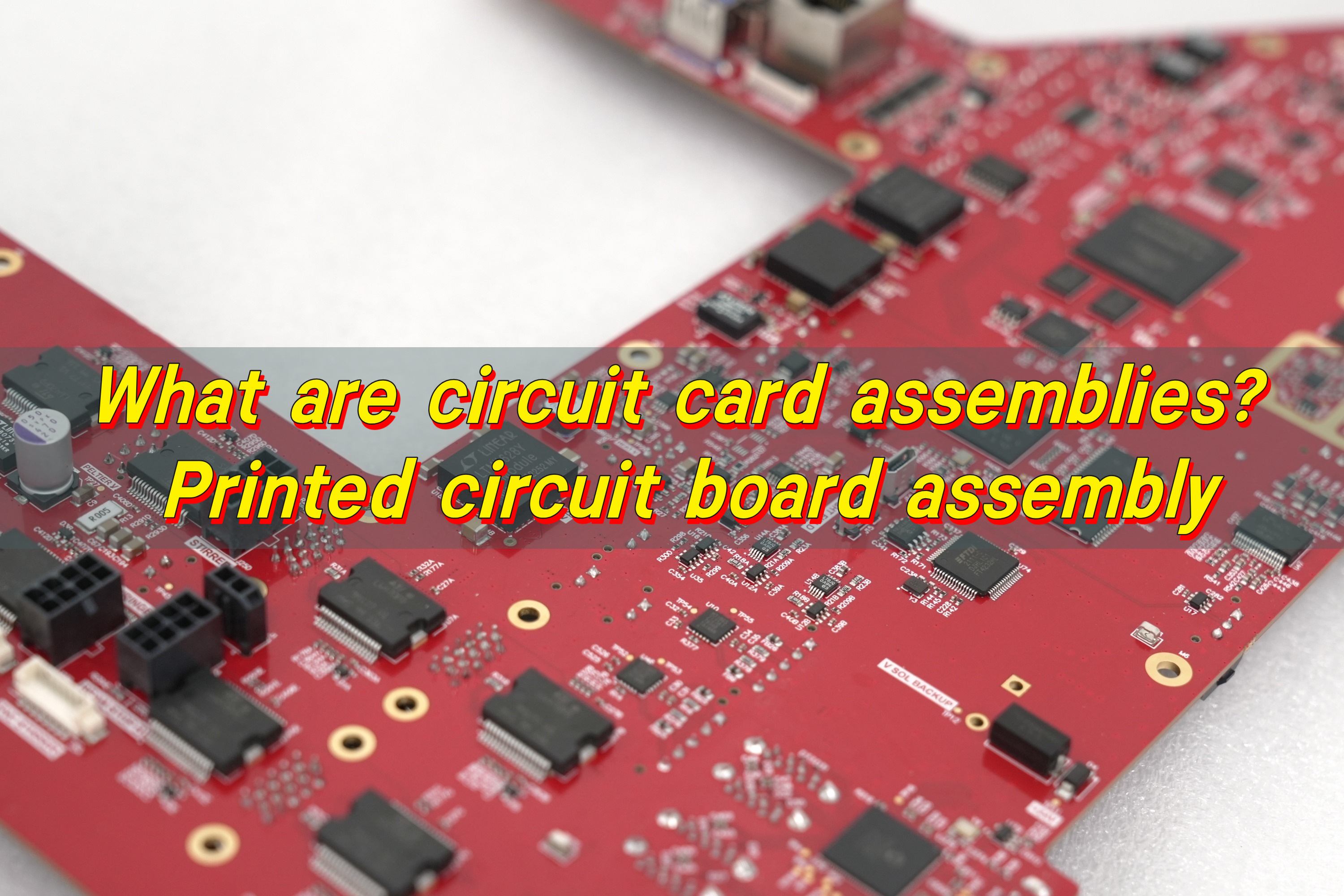
What Is an RF PCB Manufacturer?
An RF PCB manufacturer is a PCB supplier with specialized expertise in producing circuit boards for applications operating at radio frequencies, typically above 30 MHz. At these frequencies, PCB traces act as transmission lines, and small variations in geometry or material properties can significantly affect signal integrity.
Compared with standard PCB manufacturers, RF PCB manufacturers must control:
Dielectric constant (Dk) stability across frequency and temperature
Dissipation factor (Df) to minimize insertion loss
Tight impedance tolerance, often ±5% or better
Copper surface roughness, which directly affects high-frequency loss
Stackup symmetry and lamination consistency
These requirements mean RF PCB manufacturing is as much an electromagnetic discipline as a mechanical one.
What Is an RF PCB Manufacturer?
RF PCB vs Standard PCB (Quick Comparison)
Although RF PCBs and standard PCBs may look similar in appearance, they are fundamentally different in design philosophy, material selection, and manufacturing control. As frequency increases, even small variations that are acceptable in standard PCBs can cause severe performance degradation in RF designs.
Key Differences Between RF PCB and Standard PCB
Comparison Item
RF PCB
Standard PCB
Typical operating frequency
>30 MHz up to GHz/mmWave
DC to low-speed digital
Signal behavior
Transmission-line dominated
Lumped-circuit dominated
Primary design concern
Impedance, loss, phase stability
Connectivity and routing
Core materials
Rogers, PTFE, Taconic, RF laminates
FR-4
Dielectric constant (Dk)
Tightly controlled, frequency-stable
Wider tolerance
Dissipation factor (Df)
Low-loss required
Less critical
Copper surface roughness
Strictly controlled
Usually not critical
Impedance tolerance
±5% or tighter
±10% common
Stackup complexity
High, often hybrid
Relatively simple
Manufacturing difficulty
High
Moderate
Cost sensitivity
Performance-driven
Cost-driven
In short, standard PCB manufacturing prioritizes manufacturability and cost, while RF PCB manufacturing prioritizes electrical performance and consistency. This is why RF PCBs must be produced by a qualified RF PCB manufacturer rather than a general PCB supplier.
What Frequency Range Is Considered RF in PCB Manufacturing?
In PCB manufacturing, RF generally refers to frequencies above 30 MHz, where wavelength becomes comparable to trace dimensions and transmission-line effects dominate.
Typical frequency classifications include:
30 MHz – 300 MHz: VHF
300 MHz – 3 GHz: UHF and microwave
3 GHz – 30 GHz: Microwave and millimeter-wave
As frequency increases, the impact of dielectric variation, copper roughness, and impedance mismatch becomes more severe, requiring stricter manufacturing controls.
Common RF PCB Materials
Material selection is one of the most important responsibilities of an RF PCB manufacturer. RF materials are chosen for predictable dielectric behavior and low signal loss across frequency.
Typical RF PCB Materials
Rogers RO4003C / RO4350B – Widely used RF laminates with stable Dk
Rogers RO3003 / RO3006 – Microwave and millimeter-wave applications
Lack of RF-specific design-for-manufacturing review
Experienced RF PCB manufacturers reduce these risks through upfront engineering validation and strict process control.
Why Choose EBest Circuit (Best Technology) as Your RF PCB Manufacturer?
When evaluating RF PCB manufacturing capability, EBest Circuit (Best Technology) is often selected due to its strong focus on RF and high-frequency PCB production. With experience in RF materials, controlled impedance manufacturing, and RF-focused engineering support, EBest Circuit (Best Technology) demonstrates the core capabilities expected from a professional RF PCB manufacturer.
By choosing EBest Circuit (Best Technology), customers benefit from:
Proven RF and microwave PCB manufacturing experience
Tight impedance and material control
Engineering-driven process validation
Reliable performance for high-frequency applications
For projects involving RF, microwave, or high-speed communication systems, selecting EBest Circuit (Best Technology) as your RF PCB manufacturer helps reduce technical risk and improve overall product reliability.
FAQs About RF PCB Manufacturing
1. What does an RF PCB manufacturer do?
An RF PCB manufacturer produces printed circuit boards optimized for high-frequency performance, focusing on impedance control, low signal loss, and material stability.
2. Can FR-4 be used in RF PCB manufacturing?
FR-4 may be acceptable for low-frequency RF designs, but at higher frequencies it suffers from higher loss and unstable dielectric properties.
3. Why are RF PCBs more difficult to manufacture?
RF PCBs are sensitive to small variations in materials, geometry, and processing, making manufacturing control critical.
4. Are RF PCBs more expensive than standard PCBs?
RF PCBs typically cost more due to specialized materials, tighter tolerances, and additional process controls.
In the fast-paced world of electronics, finding a reliable Switzerland PCB manufacturer is crucial for turning innovative designs into high-quality products. Whether you re working on medical devices, industrial controls, or consumer electronics, choosing the right Switzerland PCB manufacturercan make or break your project timeline and performance. As a leading Global PCB Manufacturer, we understand the unique demands of the Swiss market, precision, reliability, and efficiency are non-negotiable. We combine 19 years of industry expertise with advanced manufacturing technologies to deliver PCB solutions that meet the strictest standards, from rapid prototyping to large-scale production. Our commitment to transparency and quality has made us a trusted choice for businesses across Switzerland and beyond.
Are You Facing the Following Problems?
PCB prototypes take too long to deliver, delaying your product development cycle and market launch opportunities.
Design flaws are only discovered during production, leading to costly rework and extended timelines.
Manufacturers quote low initial prices but add hidden fees for testing, materials, or urgent processing later.
Small-batch orders are rejected or charged exorbitant fees, making it hard to validate new product designs.
PCB quality is inconsistent, with frequent issues like poor solderability or impedance mismatches affecting product performance.
Lack of clear communication channels, leaving you in the dark about your order progress.
Full-Process Guarantee from Requirement to Delivery
We understand that every challenge in PCB manufacturing can impact your business success, that’s why we’ve built a full-process service system to address these pain points head-on. For slow prototyping, we’ve dedicated 7 rapid production lines and an intelligent scheduling system to ensure 12-hour urgent delivery for simple boards and 24-48 hours for most prototyping needs, cutting your development cycle in half. To avoid design-related rework, our 50+ senior engineers provide free DFM (Design for Manufacturability) analysis within 2 hours of receiving your files, identifying potential issues like line width errors or via placement problems before production starts.
Transparency is at the core of our pricing, we provide detailed quotes that include all materials, processing, testing, and packaging costs, with a strict “no hidden fees” commitment. Whether you need 1 piece for prototyping or 10,000 pieces for mass production, we accept all order sizes with consistent quality and fair pricing. Our real-time order tracking system lets you check production progress anytime, and a dedicated account manager is available 24/7 to answer your questions. From design review to final delivery, we take care of every detail so you can focus on what you do best—innovating.
Why Choose EBest Circuit (Best Technology) for Global PCB Manufacturer?
Reasons why choose EBest Circuit (Best Technology) for global PCB manufacturer:
19 Years of Industry Insight – No Guesswork: We’ve delivered 100,000+ PCB solutions for Swiss medical devices, automotive electronics, and industrial controls. Our team knows the strict DIN/IPC standards your projects demand, so we avoid costly “learning curves” common with new manufacturers.
All PCB Types Under One Roof – Save Coordination Time: From rigid FR-4 boards for industrial sensors to flexible PCBs for wearable devices and HDI boards for compact medical tools, we handle it all. No need to juggle 3+ suppliers for different prototypes.?
Precision That Meets Your CAD Files – 99.8% First-Pass Yield: Our 64-layer capacity, 3mil line width/0.1mm aperture precision, and AI-powered impedance control mean your complex designs (even for high-frequency communication boards) translate perfectly to physical PCBs. We match your Gerber files down to the micron.?
Transparent Pricing – No Hidden Bills: Our quotes include material upgrades (e.g., Rogers high-frequency substrates), AOI testing, and Swiss domestic shipping – no “surprise” fees for compliance or urgent adjustments. 85% of our repeat clients cite “cost predictability” as a top reason to stay.?
Quality That Passes Your Lab Tests – ISO 13485/IATF 16949 Certified: Every batch goes through X-Ray inspection (for BGA joints), flying probe testing (100% electrical coverage), and temperature cycling (-40°C to 125°C). We provide a full test report with your order – ready for your quality audit.?
Free DFM Analysis – Fix Issues Before They Cost You: Our senior engineers (average 12+ years experience) review your design within 2 hours, flagging issues like via placement errors or thermal stress points. This cuts rework time by 70% and gets your prototype to testing faster.?
One-Stop Service – From CAD to Your Bench: We handle design tweaks, prototyping, small-batch production, and even SMT assembly (01005 components supported). Upload your files by 3 PM CET, and get a prototype quote the same day.?
1-Piece Orders Welcome – Test Ideas Without Overhead: We never penalize innovation. Our 1-piece prototyping (starting at €49) lets you validate new designs on a budget, while our scalable production lines seamlessly ramp up to 10,000+ units when you’re ready to launch.
Top Switzerland PCB Manufacturer List
Company Name
Main Business
Process Capability
Lead Time
EBest Circuit (Best Technology) Co.,Ltd
PCB prototyping, small-batch production, mass production, HDI board manufacturing, custom PCB design support
Match Process Capabilities to Your Design: List your non-negotiable specs first—layer count, minimum line width/spacing, aperture size, and special processes (like impedance control or blind vias). Ask the manufacturer to provide test reports for similar projects to avoid mismatches.
Validate Industry Certifications: For automotive projects, confirm IATF16949; for medical devices, ISO13485 is a must. Basic ISO9001 is non-negotiable, but sector-specific certs prove they understand your compliance needs.
Test Their Urgent Order Reliability: Ask for their real on-time delivery rate (not just marketing claims) for prototypes (1-4 layers) and complex boards (16+ layers). Inquire about backup production lines for last-minute design tweaks.
Dig Into Pricing Transparency: Demand a breakdown that includes materials, processing, testing (AOI/X-Ray), and Swiss domestic shipping. Clarify if there are extra fees for urgent changes or compliance documentation—hidden costs kill project budgets.
Assess Technical Support Speed: Send a sample DFM question (e.g., “How would you optimize this thermal via placement?”) and track response time. A team that replies within 4 hours (during CET working hours) saves you weeks of delays.
Check Peer Reviews & Industry Case Studies: Look for clients in your field—an aerospace PCB maker may not excel at consumer electronics. Ask for references or case studies showing how they solved similar design challenges.
Confirm Flexible MOQ Policies: Innovation shouldn’t cost extra. Ensure they accept 1-piece prototyping without markup, and can scale seamlessly from 10 units (validation) to 10,000 units (mass production).
Clarify After-Sales Commitments: Get their defect handling process in writing. Reliable partners will offer a 48-hour root-cause analysis for faulty boards and cover rework/shipping costs for their mistakes.
Core Pain Points of PCB Manufacturing Company Switzerland
Order fragmentation leads to low production efficiency for manufacturers, resulting in longer lead times for small-batch and prototype orders.
High requirements for precision and reliability in industries like medical and automotive increase manufacturing difficulty and quality control costs.
Fluctuations in raw material prices (such as copper foil and high-frequency substrates) lead to unstable PCB pricing.
Lack of real-time production data sharing makes it difficult for customers to track order progress, causing communication inefficiencies.
Inadequate technical support from manufacturers results in frequent design-manufacturing mismatches, increasing rework rates.
Stringent environmental regulations in Switzerland raise production costs for manufacturers, which are often passed on to customers.
Shortage of professional PCB engineers leads to slow response to complex technical requirements.
How to Evaluate a Switzerland PCB Manufacturer’s Production Capacity?
1. Equipment Strength: Focus on Configuration and Advancement: Ask for a detailed equipment list (brand + model) — laser drilling machines, automated laminators, and high-speed SMT lines indicate higher precision. Request video factory audits to check if equipment is in normal operation, not just stored.
2. Quantitative Capacity: Verify with Actual Data: Don’t just ask “monthly output” — demand specific metrics like “15,000 square meters of 1-16 layer PCBs per month” or “300+ prototype models daily”. Request 3-month production reports to avoid capacity overstatement.
3. Process Coverage: Match Your Core Needs: Confirm if they handle your must-have processes (e.g., blind/buried vias for HDI boards, thick copper for power supplies). Ask for case studies — e.g., “How many 64-layer PCBs did you produce last quarter?”.
4. Material Compatibility: Cover Your Substrate Requirements: Check if they work with your materials (FR-4, Rogers high-frequency substrates, flexible PI). Reliable manufacturers have authorized partnerships with top material suppliers (e.g., Isola, Panasonic).
5. Scheduling Efficiency: Prioritize Digital Systems: Choose manufacturers using MES (Manufacturing Execution System) — it enables real-time order tracking and reduces scheduling errors. Ask: “How quickly can you adjust production for a 24-hour urgent order?”.
6. Urgent Order Capability: Count Dedicated Lines: The number of rapid prototyping lines directly affects delivery — 5+ dedicated lines mean they can handle urgent orders without delaying mass production. Confirm their shortest lead time (e.g., 12-hour for 2-layer boards).
7. Supply Chain Stability: Check Key Material Partnerships: Ask for a list of long-term suppliers (e.g., copper foil, solder mask). Manufacturers with 3+ years of cooperation with tier-1 suppliers avoid production halts due to material shortages.
8. Team Competence: Engineers Determine Problem-Solving Ability: Inquire about the ratio of senior engineers (10+ years experience) — it should be over 30%. Test their responsiveness with a technical question (e.g., “How to optimize impedance control for 5G PCBs?”).
How to Evaluate the Quality Control of a Switzerland PCB Manufacturer?
Evaluation Guide to the Quality Control of Switzerland PCB Manufacturer:
1. Certifications: Prioritize sector-specific certifications over basic ones, automotive needs IATF16949, medical requires ISO13485, and aerospace demands AS9100. Ask for a copy of the certification (not just a logo) and verify its validity via the issuing body’s database.?
2. Testing Equipment: Ensure they have AOI (for solder joint defects), X-Ray (for BGA internal connections), flying probe testers (for 100% electrical coverage), and environmental chambers (for temperature/humidity tests). Request calibration reports for key equipment—expired calibration renders test results useless.?
3. Incoming Material Inspection (IQC): They must conduct 100% inspection on substrates, copper foil, and solder mask. Ask for IQC records (e.g., material test reports from suppliers + in-house check data) and confirm their suppliers are tier-1 (e.g., Isola, Rogers) to avoid substandard raw materials.?
4. In-Process Control: For critical steps like lamination and electroplating, check if they use real-time monitoring (e.g., temperature/pressure sensors for lamination). Ask for a process control plan (PCP) that outlines sampling frequency—at least 1 sample per 50 boards for high-layer PCBs.?
5. Finished Product Testing: They must perform electrical testing (open/short), appearance inspection (per IPC-A-600 standard), and impedance testing (if your design requires it). Insist on a batch-specific test report that includes pass/fail data and inspector signatures—no report = untested.?
6. Defect Metrics: Request their last 6 months’ DPPM (Defects Per Million Opportunities) — reliable manufacturers have DPPM ≤ 200 for industrial PCBs. Also, check customer complaint rates—anything above 0.5% indicates inconsistent quality.
7. Traceability System: A robust system lets you trace a PCB’s material batch, production operator, testing results, and even equipment used—via a unique batch number. Test this by asking: “Can you show me all data for batch #XXX from 3 months ago?”
8. Quality Issue Handling: Confirm they provide a written process: 48-hour root-cause analysis for defects, 72-hour solution proposal, and compensation for their errors (e.g., free rework + shipping). Avoid manufacturers with vague “case-by-case” policies.
How to Evaluate a Switzerland PCB Manufacturer’s Lead Time?
1. Confirm Standard Lead Times with Layer-Specific Data: Ask for a categorized lead time table (e.g., 1-4 layers, 5-16 layers, 17-64 layers) instead of vague statements. Compare with Swiss industry benchmarks—reliable manufacturers deliver 1-4 layer prototypes in 24-48 hours, 5-16 layers in 3-7 days, and mass production in 7-15 days (reference data from top local manufacturers).
2. Verify Urgent Delivery Capabilities & Cost Transparency: Clarify the shortest lead time for urgent orders (e.g., 12-hour for 2-layer boards) and confirm if there are tiered fees (e.g., 20% surcharge for 24-hour delivery vs. 50% for 12-hour). Ask for a written urgent service agreement to avoid post-order price hikes.
3. Assess Scheduling Flexibility for Priority Adjustments: Test with a scenario: “If I need to prioritize my 100-piece order over an existing batch, how quickly can you adjust?” Reliable partners will have a clear priority mechanism (e.g., dedicated rapid lines) instead of vague “try our best” promises.
4. Check On-Time Delivery Rate with Actual Records: Request the last 6 months’ delivery data (not just customer reviews) , focus on on-time rate for orders with similar complexity to yours. A rate ≥95% is acceptable; top manufacturers maintain ≥98% for standard orders.
5. Demand Contingency Plans for Common Delays: Ask specific questions: “What if your laser drilling machine breaks down?” or “How do you handle copper foil shortages?” Qualified manufacturers will have backup equipment (≥2 sets for key processes) and 3+ tier-1 material suppliers to avoid halts.
6. Evaluate Logistics Reliability for Swiss Delivery: Confirm their long-term logistics partners (e.g., DHL, Swiss Post) and average delivery time from factory to your location. For Swiss domestic shipments, door-to-door service within 1-2 business days is standard—avoid manufacturers relying on third-party brokers with unclear timelines.
7. Validate Real-Time Tracking granularity: Ensure their tracking system covers full lifecycle: order confirmation → production start → key process completion → testing pass → shipment. Ask for a demo—top systems send automated updates (email/SMS) when the order moves to the next stage.
8. Get Delayed Delivery Compensation in Writing: Reference industry compensation standards , require clear terms: e.g., “1% discount per day delayed (max 10%) for standard orders; free rework + expedited shipping for delays caused by manufacturer.” Avoid vague “case-by-case” policies.
Frequently Asked Questions About Switzerland PCB Manufacturer
Q1: How can I reduce the cost of PCB prototyping? A1: Choose a manufacturer that offers free DFM analysis to avoid rework costs; take advantage of prototyping promotions (we offer free 1-6 layer PCB prototyping for new customers); and optimize your design to use standard materials and processes instead of custom ones.
Q2: What should I do if my PCB design has special technical requirements? A2: Communicate your requirements (such as impedance control, high-temperature resistance) with the manufacturer’s engineering team in advance; provide detailed design files and technical specifications; and ask for a pre-production sample to verify whether it meets the requirements.
Q3: How to confirm that the PCB meets the environmental protection requirements of the European Union? A3: Choose a manufacturer that can provide RoHS and REACH certification reports; confirm that they use lead-free soldering and environmentally friendly materials; and ask for a material declaration (MSDS) for key components.
Q4: What if the delivered PCB has quality problems? A4: Contact the manufacturer’s after-sales team immediately and provide photos and test reports of the defective products; reliable manufacturers will conduct a root cause analysis within 24 hours and provide solutions such as rework, replacement, or refund (we promise to bear all costs for quality problems caused by us).
Q5: Can I change the order requirements after placing the order? A5: It depends on the production progress, if the production has not started, changes can be made free of charge; if it is in the middle of production, there may be additional costs for rework. We recommend confirming the order details carefully before production, and our account manager will remind you of key points.
Struggling with PCB troubleshooting? Our definitive guide reveals the tools, techniques, and real-world case studies to diagnose and fix any board.
What Tools Are Required for PCB Troubleshooting?
The table below lists the necessary tools and their main uses to help you build a reliablePCB troubleshootingtoolkit.
Tool Name
Purpose
Multimeter
Voltage/resistance measurement
Soldering Station
Component replacement/repair
Oscilloscope
Signal integrity analysis
Logic Analyzer
Digital circuit debugging
Thermal Camera
Hidden short detection
X-ray Inspection
Via/solder joint analysis
Tweezers
Precision component handling
Magnifying Glass
Visual inspection of solder joints
Jumper Wires
Circuit bypass/signal injection testing
ESD-Safe Tools
Static protection during handling
How to Troubleshoot a Circuit Board with a Multimeter?
The digital multimeter (DMM) is the most versatile tool forPCB troubleshooting, and mastering its use can resolve 70% of common board issues. Below is a step-by-step guide to using a multimeter for troubleshooting PCB circuit board problems, from basic continuity checks to component testing.
1. Disconnect Power: Ensure the circuit board is powered off and capacitors are discharged. Safety first—avoid live measurements unless testing in-circuit voltage rails.
2. Set Multimeter to DC Voltage: Configure the multimeter to the appropriate DC voltage range (e.g., 20V scale for logic circuits). Use auto-ranging meters for flexibility.
3. Check Power Rails: Probe VCC and GND points to verify power delivery. A stable 5V/3.3V reading confirms functional power regulation. Deviations indicate regulator or capacitor issues.
4. Test Component Voltage: Measure voltage at critical components (IC pins, resistors) to identify unexpected drops. For example, a 0V reading at a microcontroller’s VCC pin suggests a broken trace or faulty regulator.
5. Continuity Test: Switch to beep/continuity mode to check for open/short circuits. Test traces between components, silence indicates a break, while a beep confirms connectivity.
6. Resistance Measurement: Verify resistor values with the ohms function. Compare measured values to datasheet specs. Unusually high/low readings indicate damaged components.
7. Diode Test: Use the multimeter’s diode mode to confirm proper diode function. A forward voltage drop of ~0.7V (silicon) or ~0.3V (germanium) indicates health. Reverse polarity should show “OL” (open circuit).
8. Document Findings: Record all measurements systematically. Track voltage readings, continuity checks, and resistance values to isolate faults and share results with teams.
PCB Troubleshooting Techniques
Beyond tool use, effective PCB troubleshooting relies on systematic techniques that eliminate guesswork. These methods help isolate problems quickly, whether you’re dealing with a simple hobby board or a complex industrial PCB.
Visual Inspection First
Before using any tools, perform a thorough visual check, many defects are visible to the naked eye (or with a microscope). Look for: burnt components (charring or discoloration), cold solder joints (dull, grainy appearance), bent pins on ICs, corrosion (common in humid environments), and loose components. This step is often overlooked but can save hours of troubleshooting PCB circuits unnecessarily.
Divide and Conquer Method
For complex PCBs, split the circuit into smaller, manageable sections (e.g., power supply, input module, output module). Test each section individually to identify which part is malfunctioning. For example, if the PCB won’t power on, first test the power supply section, if it’s working, move to the next section. This technique streamlines PCB troubleshooting by narrowing the focus.
Signal Tracing with an Oscilloscope
When dealing with intermittent issues or signal distortion, an oscilloscope is invaluable. Trace the signal from the input to the output of the circuit. Compare the actual signal to the expected signal (from the schematic). Anomalies like delayed signals, noise, or clipping will point to the faulty component or trace. This method is particularly effective for troubleshooting pcb circuit board used in high-frequency applications (e.g., communication devices).
Swap Test for Suspected Components
If you suspect a specific component (e.g., a microcontroller or capacitor) is faulty, replace it with a known-good component of the same specification. This “swap test” is quick and effective, but ensure you use the correct replacement to avoid further damage. Always document which components you swap, this helps with future PCB troubleshooting if similar issues arise.
PCB Board Troubleshooting Case Studies
Project Requirement: Isolate and resolve a persistent short circuit between the 3.3V power plane and ground in a 6-layer PCB (dimensions: 200mm × 150mm) causing intermittent system crashes during thermal stress testing.
Troubleshooting Plan:
Initial Inspection: IR thermal imaging revealed localized hotspots (ΔT = 18°C above ambient) at via #A12, indicating abnormal current leakage.
Continuity Testing: Multimeter measurements showed 0.03Ω resistance between power/ground traces at via #A12—significantly lower than the design specification of >100MΩ.
X-Ray Analysis: 3D X-ray microscopy quantified a 15μm copper bridge between adjacent vias, validated via slice-and-view SEM at 5000× magnification.
Simulation Verification: Ansys Icepak thermal simulation confirmed a 22% higher current density at via #A12 under peak load, correlating with field failure data.
Failure Replication: Accelerated life testing (1000 thermal cycles from -40°C to 125°C) reproduced failures exclusively at via #A12, confirming root cause.
Output Result:
Isolation: Laser-cut precision ablation removed the 15μm copper bridge, verified via post-repair continuity tests (resistance >1GΩ).
Validation: Post-repair thermal imaging showed normalized temperature distribution (ΔT < 5°C), and functional testing confirmed 100% recovery with zero failures over 5000 thermal cycles.
Design Improvement: Implemented via-to-plane spacing optimization (increased from 0.2mm to 0.3mm) and added solder mask webbing, reducing short-circuit risk by 92% in subsequent prototypes.
PCB Troubleshooting and Defect Analysis
Open Circuits
Cause: Incomplete etching, wire/pad fractures, or via misalignment.
Fix: Use flying probe testing to locate breaks; validate etching parameters and material integrity.
Short Circuits
Cause: Conductive debris, solder bridge formation, or layer-to-layer misalignment.
Fix: Conduct electrical testing and X-ray/AOI inspection; clean surfaces and optimize solder mask application.
Solder Joint Defects
Cause: Poor wetting, insufficient/excess solder, thermal stress, or pad lift-off.
Fix: Refine reflow profile, ensure pad design meets IPC standards, and validate component alignment.
Layer Registration Issues
Cause: Imprecise layer stacking or drill misalignment during lamination.
Fix: Verify registration marks via optical measurement; recalibrate drilling/laminating equipment.
Delamination/Blistering
Cause: Moisture ingress, inadequate lamination pressure/temperature, or contaminated prepreg.
Fix: Improve storage conditions, validate lamination parameters, and audit material quality.
Via Defects (e.g., Necking, Resin Starvation)
Cause: Inadequate plating, drill debris, or void formation.
Fix: Implement via plugging processes; optimize plating chemistry and drilling parameters.
How to Prevent PCB Board Troubleshooting?
The best PCB troubleshooting is the kind you don’t need to do. Preventive measures during design, manufacturing, and maintenance can significantly reduce the risk of PCB failures. Below are key strategies to minimize troubleshooting PCB efforts.
Robust PCB Design
Design flaws are a major cause of PCB failures. Use design rules to avoid common issues: ensure adequate trace width for current requirements (thinner traces overheat), place heat-sensitive components away from high-power devices, and include test points for easy PCB troubleshooting (e.g., at key nodes like power inputs and IC pins). Use simulation software to test the design for signal integrity and thermal performance before manufacturing.
Quality Manufacturing Processes
Work with reputable manufacturers that follow strict quality control standards. Ensure the manufacturing process includes: automated soldering (reduces human error), optical inspection (to detect solder defects), and functional testing (to verify the PCB works as intended). Ask for manufacturing reports to track potential issues (e.g., solder joint defect rates) that could lead to future troubleshooting PCB.
Regular Maintenance and Inspection
Implement a preventive maintenance schedule for PCBs in critical applications (e.g., industrial control systems, medical devices). Regular checks include: cleaning the PCB to remove dust and debris (which cause overheating), inspecting for corrosion or loose components, and testing key parameters (e.g., voltage, resistance) with a multimeter. Early detection of minor issues prevents them from becoming major failures requiring extensive PCB troubleshooting.
Proper Handling and Storage
Poor handling and storage damage PCBs before they’re even used. Store PCBs in anti-static bags to prevent electrostatic discharge (ESD), which damages sensitive components like microcontrollers. Handle PCBs by the edges (avoid touching traces or components) and use ESD wrist straps when working on them. Ensure storage areas are dry and at a consistent temperature to prevent corrosion.
Frequently Asked Questions of PCB Troubleshooting
Q1: What’s the First Thing I Should Do When Troubleshooting a PCB? A1: Start with a visual inspection and disconnect power. Check for burnt components, loose joints, or obvious defects. Disconnecting power ensures safety and prevents further damage.
Q2: How Can I Find a Short Circuit in a Multi-Layer PCB? A2: Use a multimeter in continuity mode or a circuit tracer. Identify shorted nodes via the schematic, trace paths between them, and check for hot spots with a thermal camera during low-voltage power-on tests.
Q3: Why Is My PCB Turning On but Not Functioning Correctly? A3: It’s likely a signal or component issue. Use an oscilloscope to trace signals for distortion/missing data. Test components individually with a multimeter. Common in digital device PCBs.
Q4: Can ESD Damage Cause Intermittent PCB Issues? A4: Yes. ESD can cause intermittent failures (e.g., erratic microcontrollers). Replace suspected components with known-good ones to test. Prevent damage with anti-static tools and proper storage.
Q5: How Do I Troubleshoot a PCB Without a Schematic? A5: Focus on visual inspection and basic tests. Trace power paths with a multimeter, identify key components, and use an oscilloscope to map signal paths. Document findings to create a reverse-engineered schematic.
Looking for PCB manufacturer in Austria? This blog covers list and selection guide, pain point, production capability and delivery time for PCB manufacturer in Austria.
Austria, with its robust industrial foundation and advanced technological ecosystem, has nurtured a group of high-quality PCB manufacturers. Among them, the top PCB Manufacturer in Austria stand out for their stringent quality control, innovative production techniques and reliable supply chain management. These leading PCB Manufacturer in Austria not only cater to the domestic demand from industries like automotive, aerospace and industrial electronics but also gain recognition in the European and global markets, becoming an indispensable part of the international PCB supply network.
Top PCB Manufacturer in Austria List
Company Name
Business
Advantages
Process Capabilities
Lead Time
EBest Circuit (Best Technology) Co. Ltd
2-36 layer rigid, flexible & rigid-flex PCBs for automotive, aerospace, industrial control & communication equipment
25-year industry experience; ISO 9001/IATF 16949/UL/AS9100D certifications; 10+ years technical team; 99.8% quality yield; strong European supply chain partnerships
Prioritize manufacturers supporting multi-stage HDI, high-frequency/high-speed materials (e.g., Rogers 4350B), and embedded component processes. Verify mature solutions for impedance control (±8% accuracy), blind/buried via capabilities (minimum aperture 0.1mm), and surface finishes (ENIG/ENEPIG/OSP), with IPC Class II+ certification test reports required.
2. Quality Control System
Demand dual ISO 9001/14001 certifications and automotive-grade IPC-A-600/610 compliance records. Focus on AOI optical inspection coverage (≥98%), flying probe test coverage, and reliability testing procedures (e.g., thermal shock cycles, CAF testing). Avoid “panelized” factories relying on third-party subcontracting.
3. Capacity Matching Analysis
Align production lines with project scale: for small batches (≤50㎡), confirm SMT line quantity (≥3 lines); for large batches (≥500㎡), validate AOI cycle time (≤30 seconds/panel) and maximum multi-layer press layers (≥16 layers).
4. Engineering Support Responsiveness
Require DFM feedback mechanisms, including line width/spacing limits (≥3mil), BGA pitch recommendations, impedance calculation toolchains (e.g., Polar SI9000), and NPI process timelines (DFM reports ≤48 hours).
5. Supply Chain Transparency
Audit raw material sources (e.g., CCL suppliers like Kingboard/Shengyi), critical material inventory strategies (safety stock ≥30 days), and logistics timeliness (DHL/UPS direct coverage). Confirm environmental compliance via RoHS/REACH declarations and waste recycling processes.
6. Cost Structure Transparency
Request itemized quotes including tooling, engineering, material, and NRE costs. Beware of “low-cost traps”—compare process segment Quotation difference rate (≤15%) and confirm NRE fee amortization clauses.
7. Case Validation Mechanism
Require recent 3-year the same project types (e.g., automotive/medical), focusing on end-customer names, project timelines, yield data, and post-sale issue resolution records. Verify capacity utilization (≥70%) and on-time delivery rates (≥95%) via third-party audit reports.
8. Compliance and Sustainability
Confirm EU CE certification, WEEE directive compliance, and Austrian local environmental regulations. Provide carbon footprint reports and energy-efficient equipment lists (e.g., LED lighting, heat recovery systems), with verification of EICC or similar CSR initiatives.
Core Pain Points of PCB Manufacturer in Austria
High labor costs: Austria’s strict labor regulations and high wage standards significantly increase the operational costs of PCB manufacturing, reducing profit margins compared to manufacturers in Southeast Asia.
Supply chain instability: Dependence on imported raw materials (such as copper clad laminates and solder mask) leads to risks of price fluctuations and delivery delays, especially amid global trade tensions.
Intense European competition: Facing fierce competition from PCB manufacturers in Germany, Switzerland, and other neighboring countries that also focus on high-end markets, making it challenging to expand market share.
Rapid technological iteration: The need to continuously invest in advanced equipment (such as laser drilling machines and automated assembly lines) to keep up with the demand for higher density and smaller size PCBs, increasing capital expenditure pressure.
Stringent environmental regulations: Austria’s strict environmental protection policies require manufacturers to invest heavily in wastewater treatment and waste recycling systems, adding to environmental compliance costs.
Skill shortage: Difficulty in recruiting and retaining skilled technicians specialized in PCB design, process optimization, and quality control, due to the aging workforce in the local manufacturing sector.
Fluctuating demand: The automotive and aerospace industries, major clients of Austrian PCB manufacturers, have volatile demand cycles, leading to uneven production capacity utilization.
How to Evaluate Production Capacity of PCB Manufacturing in Austria?
1. Assess manufacturing scale: Production scale directly determines capacity ceiling and order undertaking ability. Investigate core indicators like factory area, number of production lines, and annual output (calculated by square meters or units) to confirm basic capacity and scalability.
2. Examine equipment configuration: Equipment level is the foundation of production efficiency. Check types, brands and service life of key equipment (e.g., PCB etching machines, drilling machines, AOI systems) to judge technical maturity and stable production capability.
3. Review process certification: Certifications reflect standardized management level. Verify authoritative certifications such as ISO 9001, IATF 16949 and UL, which are direct proofs of reliable production processes.
4. Analyze sample quality: Sample precision mirrors mass production level. Test prototypes to evaluate line accuracy, via reliability and surface finishing quality, these indicators directly show manufacturing precision.
5. Check production lead time: Lead time reflects scheduling efficiency. Inquire about prototype and mass production lead times; reasonable and stable cycles indicate scientific production planning and smooth process links.
6. Evaluate quality control system: Strict QC ensures product consistency. Understand full-process inspection links (incoming material, in-process, final inspection) and defective product rate (PPM) to avoid batch quality risks.
7. Reference customer cases: Cooperation experience with high-end clients proves capability. Review cooperation history with large enterprises in automotive and aerospace industries to confirm adaptability to strict requirements.
8. Assess R&D capability: R&D strength guarantees technical support. Investigate R&D team size, patent quantity and custom solution experience to ensure adaptation to new technology and product demands.
How to Evaluate Delivery Time of PCB Manufacturers in Austria?
1. Clarify standard lead time with industry benchmarks:
Confirm the manufacturer’s standard delivery cycle for different PCB types, and compare it with Austria’s PCB industry averages. For example, rigid PCB prototypes generally take 7-12 working days (industry average: 9 days), flexible PCB prototypes 5-8 working days (industry average: 6.5 days), and mass production of 10,000-piece rigid PCBs 15-25 working days (industry average: 20 days). Ensure the cycle matches your project’s critical path schedule.
2. Quantify emergency response capability:
Inquire about the manufacturer’s urgent order processing capacity, including the maximum compression ratio of the cycle and additional cost standards. Qualified Austrian manufacturers can shorten the lead time by 30%-50% for urgent orders (e.g., reducing 10-day prototypes to 4-5 days), with additional costs ranging from 15%-30% of the original order value. It is recommended to confirm the proportion of urgent orders the factory can undertake (ideally no more than 15% of monthly output to avoid affecting normal production).
3. Evaluate supply chain stability with inventory data:
Focus on the manufacturer’s raw material inventory turnover rate and safety stock level. Excellent suppliers have a copper-clad laminate inventory turnover rate of ≥8 times/year, and key materials (such as solder mask and conductive ink) maintain a 15-20 day safety stock. This can reduce the risk of delivery delays caused by raw material shortages, which accounts for 42% of delivery problems in Austria’s PCB industry.
4. Demand transparent production scheduling with update frequency:
Require the manufacturer to provide real-time production progress updates, with a standard update frequency of once every 4 hours for urgent orders and once a day for regular orders. Advanced factories use MES systems to share scheduling data, enabling customers to check the order status independently, which can reduce communication delays by 60%.
5. Verify on-time delivery rate (OTDR) with historical data:
Request the manufacturer’s past 6 months of OTDR reports. The industry excellent level in Austria is ≥95%, and the qualified level is ≥90%. For orders with delivery delays, confirm the average delay duration (should be ≤3 working days) and compensation mechanism (e.g., 0.5%-1% of the order value per day of delay).
6. Optimize logistics efficiency with transportation data:
Understand the manufacturer’s cooperative logistics providers and average transportation time. For European customers, domestic transportation in Austria takes 1-3 days, and cross-border transportation to Germany, Switzerland, etc., takes 2-5 days. Choosing suppliers with bonded logistics qualifications can shorten customs clearance time by 2-4 days.
7. Stipulate clear contract terms with data indicators:
Clearly write the delivery time (accurate to the working day), OTDR guarantee (≥92% as the minimum requirement), and penalty clauses in the contract. For example, if the OTDR is lower than 90%, the manufacturer shall bear a penalty of 2% of the total order value, which can reduce delivery disputes by 75%.
Core Direction: Driven by AI computing power, demand surges for advanced HDI (e.g., mSAP semi-additive process), ultra-multilayer boards (20+ layers), IC substrates, and flexible circuits. For instance, NVIDIA Rubin platform requires M9-grade substrates (quartz-based), with line width/spacing compressed below 30μm, boosting single-board value by 50%-100%.
Material Innovation: Low-Dk (≤3.15) and low-Df (≤0.0007) M8.5/M9 substrates become standard, paired with HVLP4 copper foil (monthly demand up to 3,000 tons, supply gap 25%-42%) and lead-free/halogen-free materials to meet 800G/1.6T switch and ASIC server high-speed transmission needs.
Market Demand: Structural Growth in High-End Applications
AI & Automotive Electronics: AI server PCB layers rise from 24 to 30+, while automotive electronics (ADAS, high-voltage platforms) drive 15% increase in per-vehicle PCB usage. Medical devices maintain stable demand for high-precision PCBs.
Regional Shift: Supply chains expand to Southeast Asia (e.g., Thailand, Vietnam), but Austrian firms retain dominance in high-end markets via technical expertise (e.g., AT&S’s semiconductor packaging substrates) and EU environmental compliance advantages.
Environmental Compliance: Green Manufacturing Mandatory
Policy Drivers: EU regulations (RoHS, REACH, PFAS restrictions, carbon footprint laws) enforce lead-free, halogen-free material adoption and dynamic waste emission controls. Austrian firms optimize energy use via digital twin technology, e.g., carbon-based composite substrates reducing production energy consumption to align with EU Green Deal.
Smart Manufacturing: Automation & Data Integration
Production Innovation: AI-driven process optimization, laser direct imaging (LDI), ultra-fast laser drilling (precision ≤0.1mm), and full AOI/X-ray inspection raise yield rates to 99.8%. Industry 4.0 architectures enable supply chain data interoperability for dynamic capacity-demand matching, with digital twin simulations of thermal-mechanical-electrical performance shortening iteration cycles.
Material Security: Critical materials (HVLP copper foil, low-Dk glass cloth) rely on imports, but Austrian firms mitigate geopolitical risks via diversified supply systems (e.g., Taiwanese/Japanese partners) and local capacity reserves (e.g., AT&S Austria plants).
Customer-Centric Response: Rapid customization support, e.g., flexible PCB production cycles compressed to 5-7 working days, with urgent orders expedited within 2 days.
Frequently Asked Questions of PCB Manufacturing in Austria
Q1: Why are PCB manufacturing costs in Austria significantly higher? A1: Austrian PCB costs are higher due to elevated labor costs, strict environmental regulations, and smaller batch production models. Prioritize Austrian suppliers for prototypes, pilot runs, and regulated products (e.g., medical/automotive), while transitioning mature designs to EU-compliant offshore factories for volume production to balance cost and reliability.
Q2: Are Austrian PCB manufacturers mainly suitable for automotive and industrial PCBs? A2: While Austria excels in automotive, railway, power electronics, and industrial control sectors (requiring IATF 16949, long lifecycle support, and traceability), its suitability extends to low-to-mid volume, high-reliability projects. For large-scale production, buyers often qualify offshore suppliers meeting EU automotive-grade standards at lower costs.
Q3: Can PCB manufacturers in Austria handle advanced technologies like HDI or heavy copper? A3: Yes, Austrian manufacturers routinely support HDI, sequential lamination, heavy copper, and complex power PCB designs. Their capacity is optimized for engineering-driven builds rather than mass production. Validate complex stackups in Austria first, then replicate approved processes with scalable offshore partners for volume ramp.
Q4: How do PCB lead times in Austria compare with Asian manufacturers? A4: Standard Austrian lead times are 10–20 working days (layer count/complexity-dependent). Fast-turn options exist but are limited. For time-sensitive projects, use quick-turn suppliers for early prototypes and rely on Austrian/EU factories for qualification builds and production stability, balancing speed with quality control.
Q5: Is it risky to source PCBs outside Austria for EU-based products? A5: Not inherently risky if suppliers adhere to EU-aligned standards (RoHS, REACH, ISO 9001/13485/IATF 16949). Key factors are process control, traceability, documentation, and communication. Enforcing these requirements ensures EU-level reliability while improving cost efficiency.
This certification confirms that PCB processes are controlled, repeatable, and audited for defect prevention rather than post-inspection.
For automotive buyers, choosing an IATF 16949 certified PCB supplier directly reduces recall risk, audit pressure, and long-term field failures.
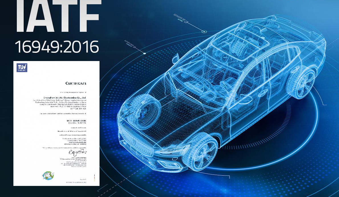
What Is an IATF 16949 Certified PCB Supplier?
AnIATF 16949 certified PCB supplier is a PCB manufacturer that complies with the global automotive quality management standard issued by the International Automotive Task Force.
This standard requires:
Full process traceability
Preventive quality planning (APQP, FMEA)
Continuous improvement and corrective action systems
Controlled production from prototype to mass volume
Unlike general certifications, IATF 16949 applies only to automotive supply chains.
What Is an IATF 16949 Certified PCB Supplier?
Why Do Automotive OEMs Require IATF 16949 PCB Suppliers?
Automotive OEMs require IATF 16949 because PCB failures can trigger recalls, safety risks, and regulatory penalties.
This certification ensures:
Stable PCB manufacturing processes
Early risk identification
Consistent quality across production lots
Audit-ready documentation for OEM and Tier-1 reviews
For safety-critical electronics, uncertified suppliers introduce unacceptable risk.
Which Automotive PCBs Must Come from an IATF 16949 Certified Factory?
Automotive PCBs that typically require IATF 16949 certification include:
Engine control units (ECU)
ADAS and camera modules
Radar and RF automotive PCBs
Battery management systems (BMS)
Power inverter and motor control boards
Safety and braking control electronics
If a PCB affects vehicle safety, emissions, or power control, certification is expected.
IATF 16949 vs ISO 9001 for PCB Manufacturing
ISO 9001 focuses on general quality procedures across industries. IATF 16949 focuses on automotive risk prevention and process stability.
Key differences for PCB buyers:
IATF 16949 requires FMEA and PPAP
ISO 9001 allows broader process variation
IATF 16949 enforces corrective action with data
ISO 9001 emphasizes documentation, not automotive reliability
ISO 9001 alone is not sufficient for automotive PCBs.
Core Capabilities Required from an IATF 16949 PCB Supplier
An automotive-qualified PCB supplier must demonstrate both engineering and process discipline.
This includes impedance-controlled stackups, material consistency, SPC monitoring, and documented change control.
Below is a technical capability table automotive buyers often request.
Capability Category
Automotive PCB Requirement
Typical Specification Range
PCB Layer Count
Multilayer & HDI
2–20 layers
Controlled Impedance
Mandatory for high-speed / RF
±5% to ±10%
Copper Thickness
Power and signal balance
0.5–6 oz
Minimum Trace / Space
Dense automotive layouts
3/3 mil
Via Technology
Reliability under vibration
Through, blind, buried, microvia
Laminate Materials
Thermal and electrical stability
High-Tg FR-4, Rogers, hybrid stackups
Surface Finish
Automotive solderability
ENIG, ENEPIG, OSP
Operating Temperature
Harsh environment tolerance
−40°C to +125°C
Traceability System
Mandatory under IATF 16949
Lot-level MES tracking
Quality Documentation
OEM audit compliance
PPAP, FMEA, Control Plan, SPC
Production Volume
Prototype to mass production
NPI → high volume
Reliability Testing
Automotive qualification
Thermal cycling, cross-section
How Traceability Works in IATF 16949 PCB Manufacturing?
In IATF 16949 certified PCB manufacturing, traceability links each PCB lot to materials, processes, inspections, and operators.
Traceability systems typically record:
Laminate batch numbers
Inner layer imaging data
Lamination cycles
Plating and surface finish parameters
Final inspection results
This allows fast containment if field issues occur.
What Quality Risks Exist Without an IATF 16949 PCB Supplier?
Choosing a non-certified PCB supplier increases:
Process variation
Incomplete documentation
Poor root-cause analysis
Audit failures during OEM reviews
These risks often surface only after volume production begins.
What Documents Should an IATF 16949 PCB Supplier Provide?
Automotive buyers should expect:
PPAP documentation
PFMEA and Control Plans
Material certifications
SPC and inspection reports
Change management records
Missing documents usually indicate limited automotive readiness.
Prototype vs Mass Production: What Buyers Often Overlook
IATF 16949 applies from the prototype stage, not only mass production.
Controlled materials, documented changes, and engineering approvals must begin early. Skipping these steps creates instability during ramp-up.
Automotive-ready PCB suppliers treat prototypes as production-intent builds.
Why Automotive Buyers Choose EBest Circuit (Best Technology) as Their IATF 16949 Certified PCB Supplier?
EBest Circuit (Best Technology) supports automotive PCB projects under IATF 16949, ISO 9001, and ISO 13485, AS9100D systems.
Our company delivers:
Automotive-grade multilayer and HDI PCBs
Controlled impedance and high-frequency designs
MES-based traceability
Structured documentation for OEM audits
Smooth transition from prototype to mass production
This combination reduces buyer risk and accelerates project approval.
FAQs
1. Is IATF 16949 mandatory for automotive PCBs?
Yes, for OEM and safety-critical automotive electronics.
2. Does IATF 16949 cover PCB prototypes?
Yes. Process control applies from early builds.
3. Can ISO 9001 replace IATF 16949?
No. ISO 9001 alone does not meet automotive standards.
4. How can buyers verify IATF 16949 certification?
Check the certificate scope, issuing body, and audit validity.
5. Why is traceability critical in automotive PCBs?
It enables fast containment and root-cause analysis during failures.
Selecting an IATF 16949 certified PCB supplier is not just a purchasing decision—it is a risk management strategy for automotive electronics. With vehicles increasingly dependent on electronics for safety, performance, and connectivity, PCB quality directly impacts system reliability and brand reputation.
This in-depth guide explains what IATF 16949 certification means for PCB manufacturing, how it affects automotive applications, how to evaluate certified suppliers, and why EBest Circuit (Best Technology) is a trusted partner for automotive PCB projects.
What Is an IATF 16949 Certified PCB?
An IATF 16949 certified PCB is a printed circuit board manufactured under a quality management system that complies with IATF 16949, the global automotive industry standard that replaced ISO/TS 16949.
Unlike general ISO 9001 certification, IATF 16949 is automotive-specific and focuses on:
Defect prevention rather than detection
Risk-based process control
Continuous improvement throughout the supply chain
Traceability and accountability at every manufacturing stage
For PCB manufacturing, this means every process—from laminate sourcing and copper plating to imaging, drilling, surface finish, and final inspection—is documented, controlled, audited, and continuously improved.
An IATF 16949 certified PCB supplier is qualified to support automotive OEMs, Tier 1 suppliers, and Tier 2 suppliers globally.
Typical Applications for IATF 16949 Certified PCBs
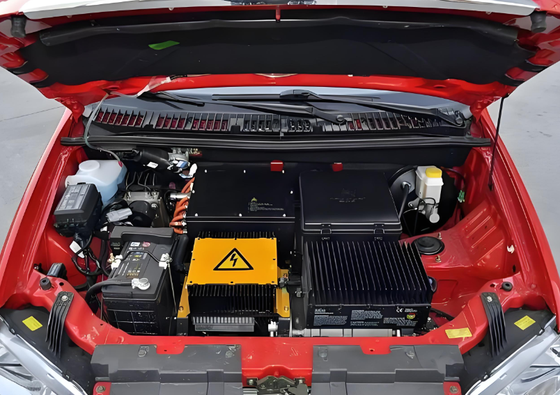
Automotive electronics operate in environments that are far more demanding than consumer or industrial electronics. As a result, IATF 16949 certified PCBs are widely used in systems where failure is unacceptable, like:
Electric vehicle (EV) systems – BMS, OBC, inverters, DC-DC converters
Body electronics – lighting control, window and seat modules
Chassis and safety systems – ABS, EPS, airbag controllers
These applications demand high reliability, thermal stability, and long service life, often exceeding 10–15 years.
Why IATF 16949 Certification Is Critical in Automotive Electronics?
Automotive PCBs must survive:
Temperature ranges from -40°C to +125°C or higher
Continuous vibration and mechanical shock
Long-term exposure to humidity, oils, and chemicals
10–20 years of operational life
IATF 16949 certification ensures that a PCB supplier has systems in place to manage these risks through:
APQP (Advanced Product Quality Planning) for new product introduction
FMEA (Failure Mode and Effects Analysis) to identify and mitigate risks
SPC (Statistical Process Control) to maintain consistency
Root cause analysis and corrective actions (8D, PDCA)
Supplier quality management for raw materials
Without IATF 16949, PCB quality may rely too heavily on final inspection rather than process stability, which is unacceptable for automotive use.
Does IATF 16949 Mean Zero Defects?
No quality standard can guarantee absolute zero defects—but IATF 16949 is designed to make defects rare, predictable, and preventable. Instead of reacting to failures, IATF 16949 requires:
Early risk identification
Process capability monitoring
Immediate corrective action when trends appear
Continuous reduction of variation
In practice, this leads to dramatically lower defect rates, improved field reliability, and reduced recall risk for automotive customers.
Does IATF Certification Automatically Mean Automotive Capability?
No, not always. IATF 16949 certifies the quality management system, not the technical capability alone.
A truly automotive-capable IATF 16949 certified PCB supplier must also demonstrate:
Experience with automotive-grade laminates (high Tg, low CTE, CAF-resistant)
Tight control of dielectric thickness and impedance
At EBest Circuit (Best Technology), our automotive PCBs are manufactured under a fully implemented IATF 16949 quality management system, ensuring process stability, traceability, and long-term reliability for safety-critical automotive electronics.
Automotive-grade epoxy, green / black / red (others on request)
Silkscreen
White, yellow (high contrast for traceability)
Panel Size
Up to 600 × 1200 mm
CAF Resistance
CAF-resistant material selection & process control
Thermal Reliability
Designed for −40°C to +125°C operating environments
Electrical Testing
Flying Probe Test, Fixture E-Test (100% testing)
Inspection
AOI, X-ray (for HDI & fine-pitch designs)
Reliability Testing
Thermal shock, thermal cycling (upon request)
Traceability
Full lot & material traceability per IATF 16949
Documentation Support
PPAP, Control Plan, PFMEA, SPC records
Our Services for IATF 16949 Certified PCB Projects
We provide comprehensive support throughout the product lifecycle:
Automotive PCB DFM and engineering review
Prototype, NPI, and mass production support
PPAP and quality documentation assistance
Long-term supply and lifecycle management
PCB & PCBA one-stop manufacturing solutions
Our goal is to help customers reduce risk, shorten development cycles, and scale confidently. If you’re searching for a dependable iatf 16949 certified pcb supplier, EBest Circuit (Best Technology) is ready to support your automotive electronics projects.
Frequently Asked Questions (FAQ)
1. Is IATF 16949 mandatory for automotive PCBs?
Most automotive OEMs and Tier 1 suppliers require IATF 16949 certification for PCB suppliers.
2. Can IATF 16949 certified suppliers support EV and ADAS projects?
Yes. IATF 16949 is widely adopted in EV, hybrid, and autonomous vehicle electronics.
3. Does IATF 16949 cover PCB assembly?
Only if PCBA is included in the certification scope. Always verify the certificate details.
4. How often is IATF 16949 audited?
Certified suppliers undergo annual surveillance audits and full recertification every three years.
Yellow discoloration on Al₂O₃ DBC substrates layers is occasionally observed after DBC bonding. For many engineers, this visual change raises a practical question: does ceramic yellowing indicate a performance risk? Why does it become yellow? This article explains the material mechanisms behind discoloration, and why it does not compromise DBC substrate reliability.
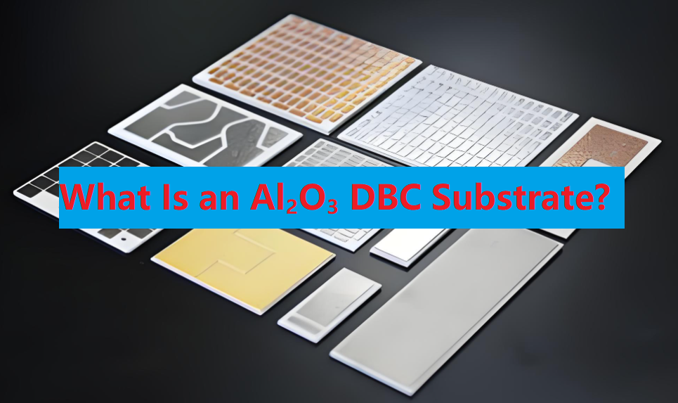
What Is an Al₂O₃ DBC Substrate?
An Al₂O₃ DBC (Direct Bonded Copper) substrate is a ceramic metal composite formed by directly bonding copper foil to an alumina ceramic plate under high temperature and controlled oxygen atmosphere.
This structure is widely used in power modules, inverters, IGBT packages, and automotive electronics, where thermal conductivity and electrical insulation are critical. The bonding process relies on interfacial chemical reactions, not adhesives.
How Does the DBC Bonding Process Work?
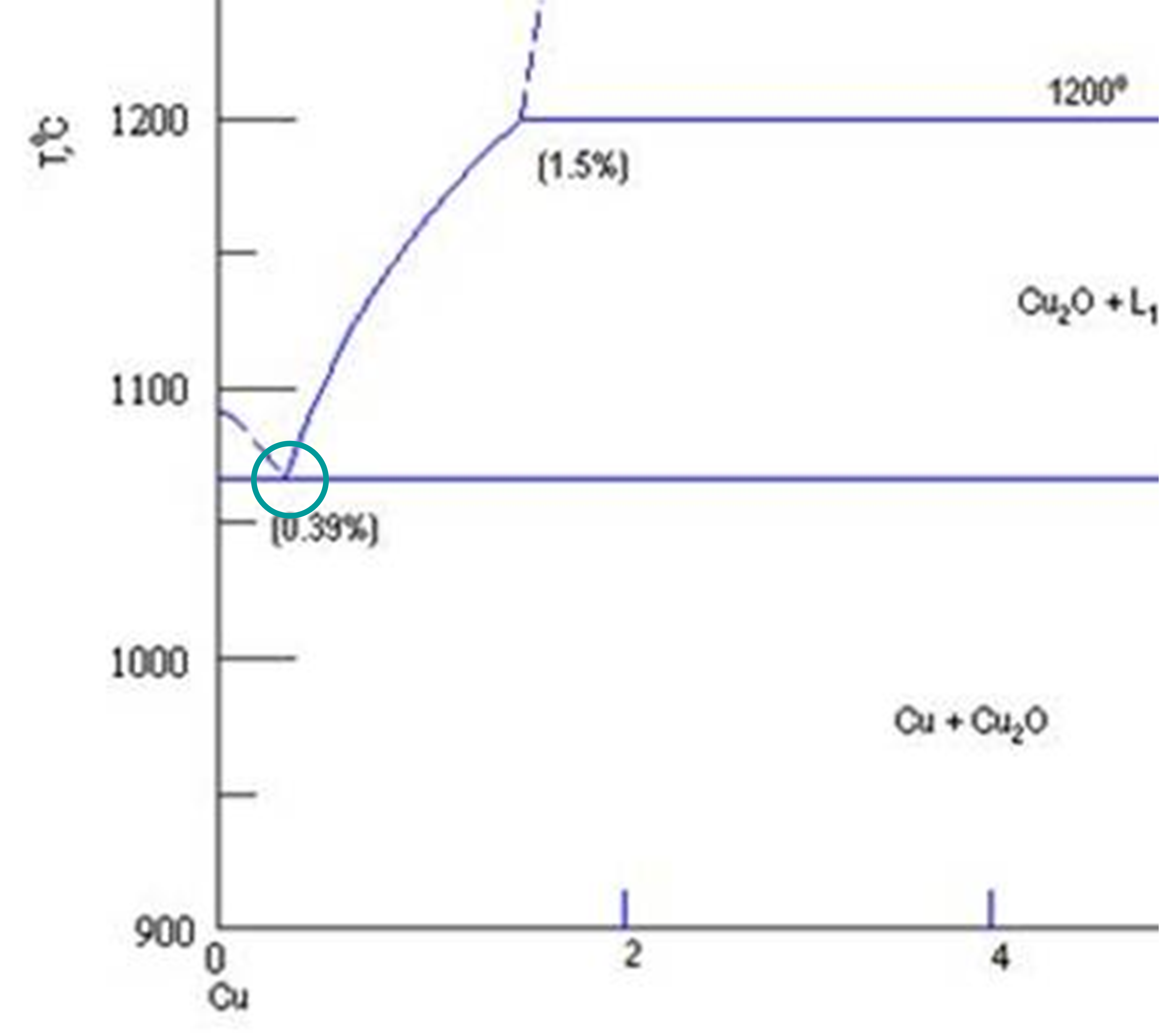
During DBC sintering, copper and alumina interact through a thermally activated oxidation-reduction mechanism.
At elevated temperatures and controlled oxygen levels:
Copper surface oxidizes to form a thin Cu₂O layer
When the temperature exceeds the eutectic point, a Cu–Cu₂O eutectic liquid phase forms
This liquid phase wets both copper and Al₂O₃ surfaces effectively
Copper oxide reacts with alumina to form CuAlO₂
The reaction can be summarized as:
Cu₂O + Al₂O₃ → CuAlO₂
CuAlO₂ acts as a ceramic-like bonding phase, enabling strong metallurgical adhesion between copper and ceramic.
What Is the Bonding Layer Made Of?
After bonding, a thin interfacial layer composed mainly of CuAlO₂ exists between copper and Al₂O₃.
Key characteristics of this layer:
Ceramic oxide with dark red to yellowish color
Excellent resistance to acids and alkalis
Difficult to remove completely using standard copper etching chemicals
When surface copper is etched away, the bonded ceramic area often appears more yellow than unbonded areas. This visual difference directly relates to the presence of the bonding layer.
Why Does Yellow Discoloration Appear on the Ceramic Surface?
Yellowing originates from two simultaneous material phenomena, both occurring during high-temperature DBC sintering.
1. Influence of the CuAlO₂ Bonding Layer
CuAlO₂ itself has a reddish-yellow ceramic appearance. Because this compound forms through interfacial reactions, its thickness is not perfectly uniform across the substrate.
Even nanometer-level thickness variation can lead to visible color differences after copper removal.
2. Migration of Ceramic Sintering Additives
Most industrial Al₂O₃ ceramics used for DBC are 96% alumina, not 100% pure.
They contain small amounts of sintering additives such as:
SiO₂
CaO
MgO
These additives improve ceramic densification during firing.
During DBC bonding:
High temperatures cause partial diffusion of these additives toward the surface
EDX analysis shows increased Si, Ca, and Mg content in yellowed areas
Higher surface concentration of these oxides correlates with yellow coloration
This behavior is consistent with ceramic sintering literature, which confirms that increased SiO₂ content can cause alumina yellowing.
How Does the DBC Bonding Process Create a Strong Interface?
DBC bonding relies on controlled oxidation and eutectic reactions at high temperature.
During sintering:
Copper forms a thin Cu₂O layer under controlled oxygen content
Above the eutectic temperature, a Cu–Cu₂O liquid phase appears
This liquid wets both copper and Al₂O₃ surfaces
Interfacial reactions form CuAlO₂, enabling direct bonding
This mechanism creates a chemically bonded interface, which is critical for long-term thermal cycling stability.
Why Is the Yellow Color Often Non-Uniform?
The discoloration is rarely perfectly even. This non-uniformity comes from reaction uncertainty, not process instability.
Key reasons include:
CuAlO₂ formation varies slightly across the bonding interface
Sintering additive diffusion is not perfectly uniform at the micro-scale
Both effects occur at nanometer-level thickness differences
Even minor variations become visible on ceramic surfaces due to light reflection and oxide color sensitivity.
Does Yellow Discoloration Affect DBC Substrate Performance?
This is the most important question for engineers and customers. Extensive testing was performed on:
DBC substrates with severe yellow discoloration
DBC substrates with minimal or no discoloration
The results show:
No meaningful difference in electrical insulation
No degradation in thermal performance
No impact on mechanical bonding strength
No reliability concerns in functional testing
In short, yellow discoloration is a cosmetic phenomenon, not a functional defect.
Their value lies in a balanced combination of electrical insulation, thermal conduction, and mechanical stability. The copper–ceramic interface is formed through a metallurgical bonding process rather than adhesives or plating.
How EBest Circuit (Best Technology) Controls DBC Substrate Quality?
Both effects occur during normal DBC sintering and may vary slightly across the substrate. Extensive testing confirms that this discoloration does not affect DBC performance or reliability.
For power electronics applications, engineering performance matters far more than visual color uniformity.
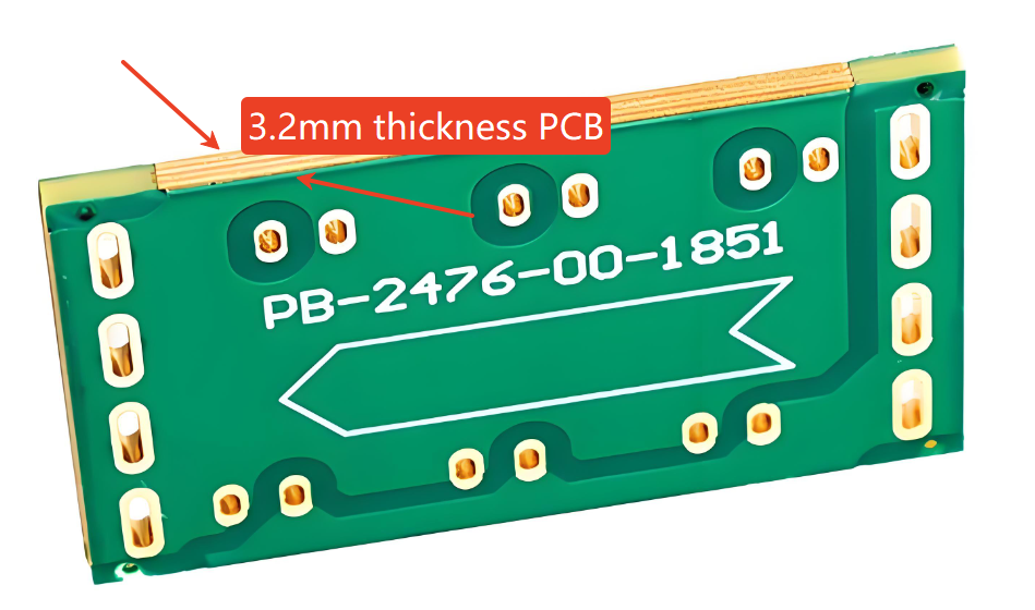
3.2mm to inches equals 0.12598 inches, commonly rounded to 0.126 inches.
lthough 3.2mm is often associated with 1/8 inch, it is slightly larger than 1/8″ (which equals 3.175mm). For general PCB fabrication, hardware selection, and sheet material, treating 3.2mm as ≈ 1/8 inch is acceptable. For tight-tolerance or mating components, always use the exact value: 0.12598 inches.
This conversion is frequently referenced in PCB thickness control, mechanical part matching, and cross-standard manufacturing, especially when metric-designed components are produced or assembled in imperial-based environments.
Engineering Method for Converting 3.2mm to Inches
All engineering-grade conversions rely on a fixed constant.
1 inch = 25.4 millimeters (exact, not approximate)
To convert millimeters to inches:
3.2 ÷ 25.4 = 0.12598 inches
In CAD systems, CAM outputs, and inspection reports, engineers usually keep four to five decimal places to prevent cumulative dimensional deviation. Rounding is applied only at the documentation or purchasing stage.
Why 3.2mm Is Widely Used in PCB and Mechanical Manufacturing?
3.2mm is considered a hybrid-standard thickness. It bridges metric design logic with imperial production habits.
In PCB manufacturing, 3.2mm is commonly selected for:
Power distribution boards
Backplanes and structural PCBs
Boards used as mounting or support elements
Industrial controller PCBs requiring stiffness
In mechanical manufacturing, 3.2mm sheet thickness is frequently used for:
Aluminum and steel brackets
Equipment enclosures
Protective covers and panels
This thickness offers good rigidity while remaining compatible with standard drilling, routing, and bending processes.
3.2mm to Inches Chart ((Fractional & Decimal)
The table below shows 3.2mm to inches alongside nearby metric sizes, including fractional inch equivalents commonly used in hardware, PCB thickness, and metal stock selection.
Millimeters (mm)
Fractional Inches
Decimal Inches
2.0 mm
5/64″
0.0787″
2.4 mm
3/32″
0.0937″
3.2 mm
≈ 1/8″
0.12598″ (≈ 0.126″)
3.5 mm
9/64″
0.1378″
4.0 mm
5/32″
0.1575″
4.8 mm
3/16″
0.1890″
6.4 mm
1/4″
0.2520″
Engineering note:
1/8 inch equals 3.175mm, not 3.2mm. The 0.025mm difference may matter in precision machining, PCB slot sizing, or press-fit applications.
Why 3.2mm Is Commonly Treated as 1/8 Inch?
In practice, 3.2mm is widely treated as a nominal 1/8-inch equivalent because:
The dimensional difference is very small
Standard drill bits and tooling align closely
PCB thickness tolerances usually exceed ±0.025mm
Hardware and sheet stock are often sold by nominal size
This is why datasheets, BOMs, and supplier listings frequently group 3.2mm and 1/8 inch together.
3.2mm to cm in Technical Documentation
3.2mm equals 0.32 cm.
This conversion is exact and does not involve rounding. It is often used in:
Engineering specifications
International standards
Educational and training materials
Centimeter notation is common in documentation intended for non-manufacturing audiences.
3.2mm to Feet in Industrial Context
3.2mm equals 0.0105 feet.
While feet are rarely used for small dimensions, this conversion may appear in:
Mixed-unit architectural layouts
Legacy documentation
Facility-level mechanical references
For fabrication work, inches or millimeters remain preferred.
Is 3.2mm the Same as 1/8 Inch in PCB and Mechanical Design?
No. 1/8 inch equals 3.175mm, not 3.2mm.
The difference is 0.025mm, which may seem negligible but can impact:
PCB edge connector fit
Slot and cutout tolerances
Press-fit components
Stack-up alignment in assemblies
In high-reliability PCB designs, this difference must be evaluated rather than assumed acceptable.
Practical PCB Applications of 3.2mm Thickness
In PCB fabrication, 3.2mm thickness is often chosen when mechanical strength is more important than weight reduction.
Typical PCB use cases include:
High-current power boards
Backplanes in industrial systems
PCBs acting as mechanical supports
Boards exposed to vibration or shock
Thicker boards reduce flexing, which helps protect solder joints and large components.
Manufacturing Implications of 3.2mm Thickness
From a production perspective, 3.2mm thickness affects multiple processes:
Drilling requires adjusted feed rates
Routing needs deeper cut passes
Plating thickness becomes more critical
Panel warpage control becomes more important
Manufacturers often adjust tooling and process parameters specifically for boards or parts at this thickness.
Metric vs Imperial Units in Global PCB Manufacturing
Most PCB designs originate in metric units. However, many:
Assembly fixtures
Test equipment
Mechanical interfaces
still follow imperial standards.
This creates frequent conversion scenarios where 3.2mm to inches must be clearly defined to avoid misinterpretation between design, fabrication, and assembly teams.
Common Engineering Errors When Converting 3.2mm to Inches
Errors often occur when:
Designers assume 3.2mm equals 1/8 inch
Finished thickness is confused with core thickness
Copper weight and surface finish are ignored
Units are converted without tolerance context
These mistakes can lead to fit issues, assembly delays, or rejected parts.
FAQs About 3.2mm to Inches
1. How many inches is 3.2mm?
3.2mm equals 0.12598 inches, which is commonly rounded to 0.126 inches for practical use. This value is widely accepted in engineering, PCB manufacturing, and hardware selection.
2. Is 3.2mm the same as 1/8 inch?
No. 3.2mm is slightly larger than 1/8 inch.
1/8 inch equals 3.175mm, while 3.2mm equals 0.12598 inches. The difference is small but can matter in precision applications.
3. Why is 3.2mm often called 1/8 inch?
3.2mm is often treated as 1/8 inch because the dimensional difference is minimal and usually falls within standard manufacturing tolerances. Many suppliers group these sizes together for convenience.
4. Is 3.2mm a standard PCB thickness?
Yes. 3.2mm is a common PCB thickness, especially for power boards, backplanes, and mechanically reinforced PCBs. It provides higher rigidity compared to thinner boards.
5. Can 3.2mm replace 1/8 inch material?
In most cases, yes.
For sheet metal, PCB panels, and brackets, 3.2mm can replace 1/8 inch. Always verify tolerance requirements for mating or press-fit parts.
6. What is the formula to convert 3.2mm to inches?
The formula is:
Inches = millimeters ÷ 25.4
3.2 ÷ 25.4 = 0.12598 inches
7. Does PCB copper thickness affect the final 3.2mm board thickness?
Yes. The finished PCB thickness includes laminate, copper layers, and surface finish. Copper weight and plating can slightly increase the final thickness beyond the nominal 3.2mm.
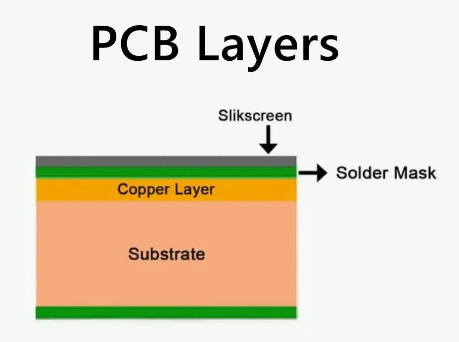
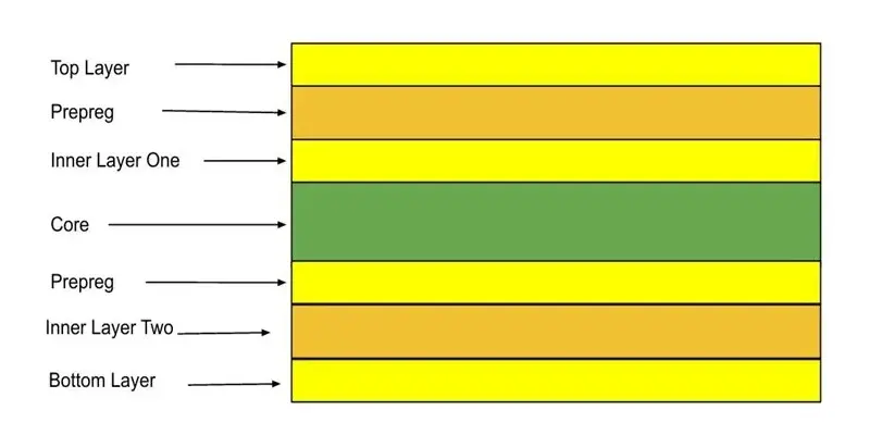
PCB layers are the physical and electrical building blocks of a printed circuit board. It is a layered structure made by stacking copper and insulating materials together. Each layer serves a clear purpose, such as carrying signals, distributing power, or providing a stable ground reference. The way these layers are arranged directly affects how the board performs.
What are layers on a PCB?
A PCB is not just a flat sheet. It is a carefully stacked structure. Each layer has a clear job. Together, these layers allow electricity to flow in a controlled way.
At the most basic level, a PCB layer can be copper, insulation, or surface coating. Copper layers carry signals and power. Insulation layers keep signals apart. Surface layers protect the board and make assembly possible.
PCB board layers define how complex a board can be. A simple product may need only two layers. A high-speed device may need many more. Each added layer increases routing space. It also improves signal control.
The layers of a PCB are planned during design. Engineers decide how many layers are needed. They also decide what each layer will do. This plan is called a PCB layer stackup.
Understanding PCB layers meaning helps avoid design mistakes. It also helps control cost. Too many layers waste money. Too few layers cause noise and routing problems.
At EBest Circuit (Best Technology), PCB layers design is part of our turnkey EMS service. From layout to final assembly, layer planning is handled early. This reduces risk and shortens lead time.
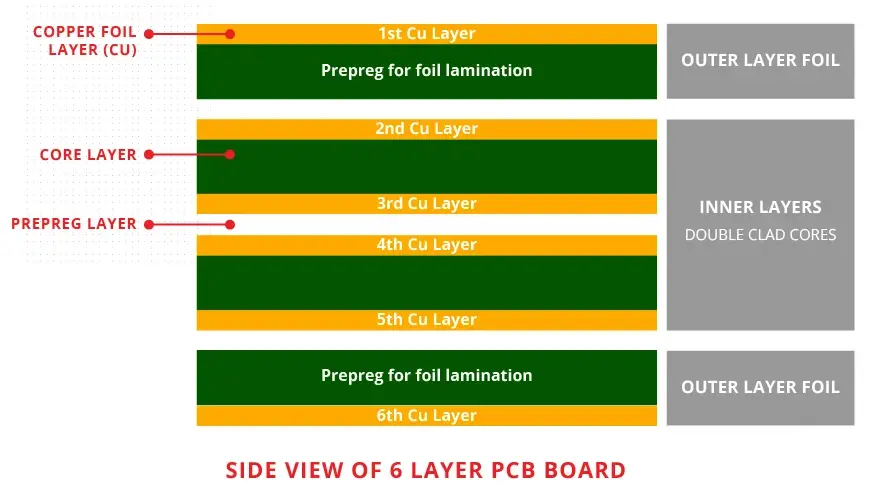
How are PCB layers produced?
PCB layers are produced through a precise and repeatable process. Each step matters. Small errors can affect the entire board.
The process starts with copper-clad laminate. This material has copper bonded to fiberglass. The fiberglass is usually FR-4. It offers strength and heat resistance.
For inner layers, copper is first etched. A photo image defines the circuit pattern. Chemicals remove unwanted copper. What remains forms the traces.
After etching, inner layers are inspected. Alignment is checked. Shorts and opens are detected early.
Next comes lamination. Multiple etched layers are stacked together. Prepreg sheets are placed between them. Heat and pressure bond everything into one board.
Once laminated, holes are drilled. These holes connect different PCB copper layers. Copper plating coats the hole walls. This creates electrical paths between layers.
Outer layers are then formed. The same imaging and etching steps apply. Finally, solder mask and surface finish are added.
Throughout this process, PCB layers stack up accuracy is critical. Even slight shifts can cause failures. At EBest Circuit (Best Technology), automated inspection ensures layer alignment stays within tight limits. Because we control both PCB fabrication and assembly, feedback is fast. That is a key benefit of turnkey EMS services.
What does a 2 layer PCB mean?
A 2 layer PCB is the most common board type. It has copper on the top and bottom. Between them is an insulating core.
In a PCB 2 layers design, components usually sit on the top. Traces run on both sides. Vias connect the two copper layers. This structure is easy to understand. It is also cost-effective. That is why many consumer products use it.
However, routing space is limited. Power and signal traces share the same layers. This can cause noise in sensitive circuits. Still, for low-speed designs, a two-layer board works well. Simple power supplies often use this type. Basic controllers also fit well.
At EBest Circuit (Best Technology), we manufacture high-quality two-layer boards at scale. Even simple boards benefit from good material and process control.
What does a 4 layer PCB mean?
A 4 layer PCB adds two inner copper layers. This design offers more control and flexibility. It is common in modern electronics.
A typical 4 layers PCB stackup includes:
Top signal layer
Inner ground layer
Inner power layer
Bottom signal layer
This structure separates signals from power. It also reduces noise. Signals return through a solid ground plane. A PCB 4 layers design allows shorter traces. It improves impedance control. This matters for fast digital signals.
In a 4 layers PCB, routing becomes cleaner. Components have more placement freedom. EMI issues are easier to manage. Cost is higher than two layers. Performance is much better.
At EBest Circuit (Best Technology), four-layer boards are a common request. They fit well in industrial control and communication products.
Do PCB layers matter?
Yes, PCB layers matter a lot. They affect performance, reliability, and cost. More layers provide better signal integrity. They allow clean power distribution. They also reduce electromagnetic interference.
Layer count affects thermal behavior. Inner planes help spread heat. This protects sensitive components.
PCB layers also affect manufacturing yield. Complex stackups need tighter control. That is why experience matters.
Choosing the wrong number of layers can cause redesigns. Redesigns cost time and money. At EBest Circuit (Best Technology), engineers review layer decisions early. This avoids later issues. It is part of our turnkey EMS approach.
How to identify PCB layers?
Identifying PCB layers depends on tools and experience. There are several common methods.
The simplest method is visual inspection. You can see top and bottom layers. Inner layers are hidden.
X-ray inspection reveals internal structure. It shows copper planes and vias. This is common in quality labs.
Another method is cross-section analysis. A small sample is cut and polished. Layers become visible under a microscope.
Design files also tell the story. Gerber files define each layer. The PCB layers name is listed clearly.
At EBest Circuit (Best Technology), every board includes a clear stackup record. This supports traceability and quality control.
Why do PCBs have multiple layers?
PCBs have multiple layers to solve real problems. Modern electronics demand more from smaller spaces.
More layers mean more routing room. Traces do not have to cross. This simplifies layout. Multiple layers also improve signal quality. Ground planes provide stable reference paths. Power planes deliver clean voltage. They reduce ripple and noise.
High-density designs require many connections. Multiple layers make this possible without enlarging the board.
In advanced devices, safety also matters. Separate layers help isolate sensitive signals. PCB design layers work together as a system. Each layer supports the others.
How many layers can a PCB have?
The number of PCB layers varies widely. Two layers are common. Four layers are standard for many products.
High-end boards may have eight, twelve, or more layers. Some specialized designs go even higher. The PCB maximum layers depend on manufacturer capability. Material choice also matters.
The PCB with most layers is usually found in servers or networking equipment. These boards handle high-speed signals and power. More layers increase cost. They also increase build time. That is why layer count should match real needs.
At EBest Circuit (Best Technology), we can manufacture PCBs with up to 32 layers. This supports complex industrial and communication systems.
How to decide PCB layer?
Deciding PCB layer count starts with function. What does the product do? How fast are the signals?
Power requirements come next. High current often needs dedicated planes.
Size constraints matter. A smaller board often needs more layers.
Cost targets guide decisions. Each extra layer adds expense.
Reliability goals also influence the choice. Stable designs often use more layers.
At EBest Circuit (Best Technology), we assist during this stage. Our team reviews design goals. We suggest practical stackups.
Conclusion:
PCB layers define how a circuit board works inside. From simple two-layer boards to complex multi-layer designs, each layer has a purpose. Choosing the right PCB layers improves signal quality, reliability, and cost control.
For technical support or project inquiries, contact us at sales@bestpcbs.com
Circuit card assemblies sit at the core of modern electronics. A circuit card assembly is a printed circuit board that has been fully populated with electronic components and soldered into place. Once assembled, it becomes a working unit capable of controlling power, processing signals, and enabling communication within an electronic device.
What Is a Circuit Card Assembly?
A circuit card assembly, often shortened to CCA, is a printed circuit board that has electronic components mounted and connected to it. These components are not loose. They are fixed, soldered, and electrically linked according to a design.
The circuit card assembly definition focuses on function. It is not just a board with copper paths. It is a working electronic unit. Once assembled, it can process signals, control power, or manage data.
Many people use the term printed circuit board assembly in the same way. In daily use, they often mean the same thing. Still, some industries prefer “circuit card assembly” because it highlights the complete, functional state.
A bare board cannot do anything alone. A circuit card assembly can. This is why CCAs are central to electronics manufacturing.
What Are the Main Components of a Circuit Card Assembly?
A circuit card assembly is a system. Every part plays a role. Each component adds a specific function, and together they create reliable operation.
The Printed Circuit Board: The printed circuit board is the foundation. It is usually made from fiberglass material like FR-4. Copper layers form electrical paths on the surface or inside the board. The board provides structure. It also controls signal flow.
Passive Components: Passive parts include resistors, capacitors, and inductors. These components shape current and voltage. They store energy, limit flow, or filter noise.
Active Components: Active components bring intelligence. These include microcontrollers, processors, and integrated circuits. They process signals. They make decisions. They control outputs.
Connectors and Interfaces: Connectors link the assembly to other systems. They allow power input, data transfer, or mechanical connection.
Solder Materials: solder joints connect everything. The quality of solder paste, reflow profile, and inspection determines long-term stability. A strong joint survives vibration and heat.
Each component matters. Together, they turn a simple board into a reliable circuit card assembly.
What Are the Different Types of CCA Assembly?
Different products need different assembly styles. Choosing the right type affects cost, size, and performance.
Through-Hole Assembly
Through-hole assembly uses components with long leads. These leads pass through holes in the board and are soldered on the opposite side.
This method offers strong mechanical bonds. It works well for large components and connectors. However, it takes more space. It also increases labor.
Surface Mount Assembly
Surface mount technology places components directly onto the board surface. No holes are needed for most parts.
This approach allows higher density. Boards can be smaller and lighter. Most modern printed circuit board assembly manufacturers focus on this method. It suits automation and high-volume production.
Mixed Technology Assembly
Some assemblies combine both methods. Sensitive or heavy parts may use through-hole, while smaller parts use surface mount.
Prototype Printed Circuit Board Assembly
Prototype assembly focuses on early design stages. Volumes are low. Speed matters more than cost. This type supports testing and refinement. Many printed circuit board assembly services specialize in fast prototype builds.
Each type serves a purpose. The best choice depends on product goals, budget, and lifecycle.
How Does a Circuit Card Work?
A circuit card assembly works by guiding electrical signals along designed paths. These paths connect components in a precise sequence.
Power enters through a connector or contact. It flows through regulators and filters. These parts stabilize voltage.
Signals then move into active components. Processors read inputs. Logic circuits decide actions. Outputs leave the board through connectors, displays, or motors. Signal integrity matters. Layout matters.
Even small design choices affect performance. Trace width, spacing, and grounding all play roles. A circuit card does not act alone. It interacts with firmware, mechanical housing, and external systems.
What Does a Circuit Card Assembly Do?
A circuit card assembly acts as the control center of an electronic device. It manages power, data, and interaction.
In some products, it handles simple switching. In others, it runs complex software. Its job is to turn input into output. Buttons become actions. Sensors become data. Signals become results.
A well-built assembly delivers stable performance. It handles heat. It resists vibration. It lasts for years.
What Are Circuit Card Assemblies Used For?
Circuit card assemblies appear almost everywhere. If a device uses electricity, it likely includes one.
Consumer Electronics: Phones, laptops, and wearables rely on compact assemblies. Surface mount printed circuit assembly manufacturing supports this demand.
Industrial Equipment: Factories use assemblies for control systems and automation. These environments demand durability.
Medical Devices: Medical equipment depends on accuracy and safety. Circuit card assemblies control imaging, monitoring, and diagnostics. Quality standards are strict. Traceability matters.
Automotive Systems: Vehicles contain dozens of assemblies. They manage engines, safety systems, and infotainment. Temperature resistance and long life are critical.
Communication Systems: Routers, base stations, and networking gear rely on high-speed assemblies. Signal integrity and layout design play major roles.
What Is the Difference Between Circuit Card Assembly and PCB Assembly?
This question comes up often. The terms are closely related, yet they emphasize different stages.
A printed circuit board is the bare board. It has copper traces and holes, but no components.
A printed circuit board assembly includes components mounted and soldered. It is functional.
A circuit card assembly usually refers to the same assembled board. The term highlights readiness for use.
In many industries, people use these terms interchangeably. Still, “circuit card assembly” often appears in defense, aerospace, and industrial sectors.
What Are the Applications of Circuit Board Assemblies?
Circuit board assemblies support modern life. Their applications keep expanding as technology evolves.
They power smart homes.
They control renewable energy systems.
They drive automation.
They support innovation.
As demand grows, so does the need for skilled manufacturers. Printed circuit board assembly manufacturers now offer advanced inspection, testing, and box build options. Box build printed circuit board assembly services go even further. They deliver complete systems, not just boards.
In global markets, China printed circuit board assembly plays a key role. Scale, experience, and supply chain strength support competitive production. With long-term manufacturing experience and a mature supply chain, BEST Technology combines regional strengths with consistent quality control, supporting both high-mix projects and volume production.
Conclusion:
A circuit card assembly is a fully populated and functional electronic board. It combines a printed circuit board with mounted components to create real performance. From consumer electronics to industrial systems, these assemblies power modern life.
For professional printed circuit board assembly services and reliable manufacturing support, contact our team at sales@bestpcbs.com