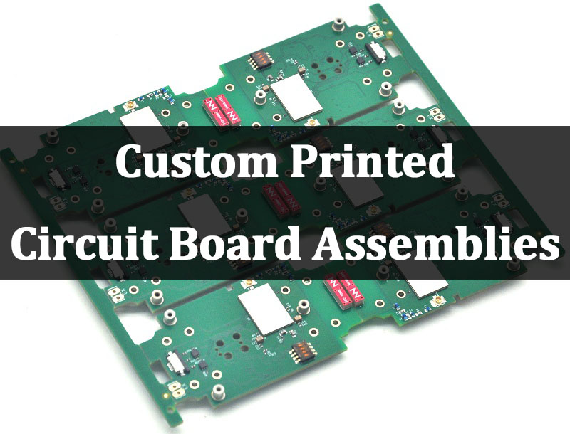
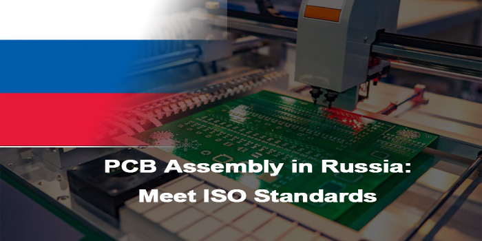
EBest – Your #1 Choice for Premium Double Sided PCB Manufacturing Since 2006
When searching for a reliable double sided PCB manufacturer, EBest stands above the rest with 20+ years of industry expertise, one-stop solutions, and global client trust.
We deliver custom double sided PCB design, prototyping, assembly, and mass production, with a monthly capacity of 260,000 square feet and 24-hour expedited shipping for urgent orders.
Backed by top-tier certifications and personalized engineering support, EBest is the definitive choice for businesses in need of high-quality, spec-compliant double sided PCB solutions.

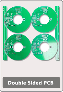
Double Sided PCB Manufacturer
Our All-Inclusive Double Sided PCB Services
- PCB Design: Custom double sided PCB design with 1-on-1 engineering support and free DFM analysis
- PCB Prototype: Rapid double sided PCB prototyping with fast turnaround and comprehensive pre-shipment testing
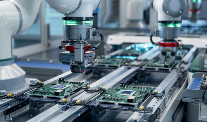
- Mass Production: High-volume double sided PCB manufacturing with consistent quality and on-time delivery
- Component Sourcing: Certified component sourcing for double sided PCB assembly, ensuring part compatibility and reliability
- PCB Assembly: Professional double sided PCB assembly (SMT/through-hole/mixed technology) with full quality inspection
- Expedited Service: 24-hour shipping for urgent double sided PCB design, prototype, and assembly orders
EBest’s Industry-Recognized Quality Certifications for Double Sided PCBs
| Certification | Applicable Industry | Core Standard |
|---|---|---|
| IATF 16949 | Automotive | Quality and reliability for automotive PCB manufacturing |
| ISO 9001:2015 | General Electronics | Global standardized quality management system |
| ISO 13485:2016 | Medical | Regulatory compliance for medical device PCB production |
| AS9100D | Aerospace & Defense | High-reliability manufacturing standards for aerospace PCBs |
| REACH | All Industries | Compliance with restricted chemical substance regulations |
| RoHS | All Industries | Hazardous material-free manufacturing processes |
| UL | All Industries | Global product safety certification |
Why EBest Is The Best Choice For Your Double Sided PCB Projects
EBest’s unrivaled focus on double sided PCB excellence addresses every client pain point with tangible, industry-leading advantages.
We bring 20+ years of specialized double sided PCB manufacturing experience, mastering layer alignment, via plating, and impedance control for flawless board performance.
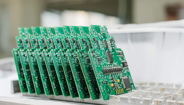
Our 260,000 sq. ft. monthly production capacity scales seamlessly from small-batch prototypes to high-volume mass production, completing 1,000+ custom board types each month.
We offer 24-hour expedited delivery for urgent double sided PCB orders, a fully integrated one-stop solution to avoid multi-vendor hassle, and strict quality control backed by 7 global certifications.
Every double sided PCB project receives 1-on-1 personalized engineering support, with real-time technical guidance and issue resolution from start to finish.
Double Sided PCB Design – 1-on-1 Support & Free DFM Analysis
Designing double sided PCBs comes with unique hurdles: misaligned vias, poor impedance control, inefficient component placement, and manufacturability gaps top the list of key challenges.
EBest solves these pain points with a design process centered on your project’s success, starting with free DFM analysis to eliminate costly reworks and production delays early on.
Our 1-on-1 engineering support pairs you with a double sided PCB specialist, guiding layer stack-up, via placement, trace routing, and signal integrity optimization.
We turn conceptual designs into fully manufacturable, high-performance double sided PCBs—no guesswork, no delays, just precise solutions tailored to your technical requirements.
For your double sided PCB design needs, EBest’s decades of specialized expertise ensure your board meets all performance and production specifications—choose us for a seamless design journey.
What Key Considerations Drive Great Double Sided PCB Design?
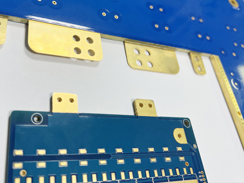
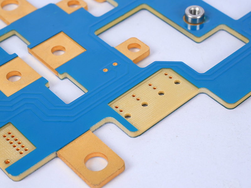
- Via Plating & Alignment: Full copper plating and precise layer alignment prevent signal loss and connectivity failures in double sided PCBs.
- Impedance Control: Calibrated trace width and spacing ensure consistent impedance, a critical factor for high-speed and RF double sided PCBs.
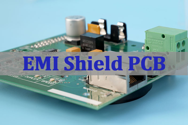
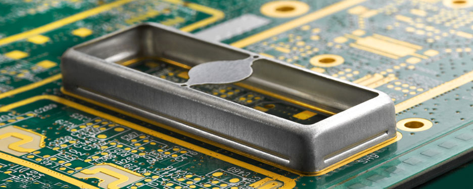
- Component Placement: Separating high-power and low-signal components on double sided PCBs minimizes electromagnetic interference (EMI).
- Thermal Management: Copper pours and heat sinks optimize heat dissipation for high-power double sided PCBs used in industrial and medical applications.
- Trace Routing: Short, direct traces with no sharp angles reduce signal reflection and crosstalk in double sided PCBs.
Double Sided PCB Prototype – 24H Expedited Delivery & Free Testing
Double sided PCB prototyping is make-or-break for product development, with slow turnaround times, design mismatches, and lack of comprehensive testing being the biggest client frustrations.
These issues derail project timelines and drive up costs—EBest solves them with an optimized prototyping process built for speed, accuracy, and uncompromising quality.
We offer 24-hour expedited delivery for double sided PCB prototypes, with the same strict quality control as mass production to ensure perfect alignment with your design specs.
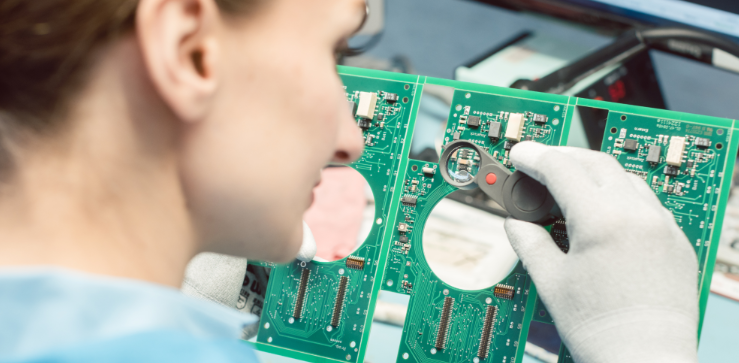
Our free pre-shipment testing includes continuity checks, short circuit detection, and visual inspection, verifying the functionality of every double sided PCB prototype.
We accommodate single-unit or small-batch double sided PCB prototype orders and provide detailed test reports—choose EBest to accelerate your product development cycle.
What Is EBest’s Double Sided PCB Prototype Testing Process?
- Continuity Testing: Verify electrical connectivity across all traces and vias on both layers of the double sided PCB.
- Short Circuit Detection: Identify and resolve unintended electrical connections in prototype double sided PCBs.
- Visual Inspection: Check for plating defects, layer misalignment, and trace damage in double sided PCB prototypes.
- Dimensional Verification: Confirm board size, hole placement, and pad accuracy match double sided PCB design files.
- Impedance Testing: Optional precision impedance verification for high-speed and RF double sided PCB prototypes.
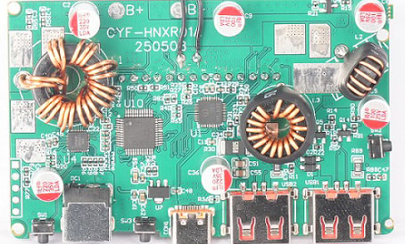
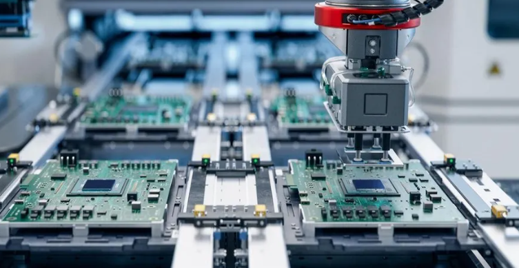
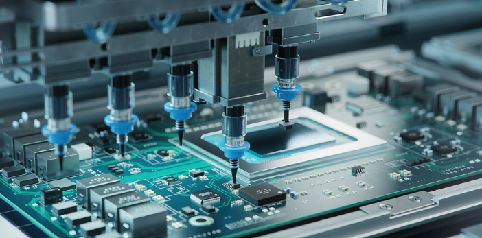
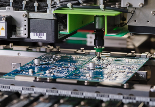
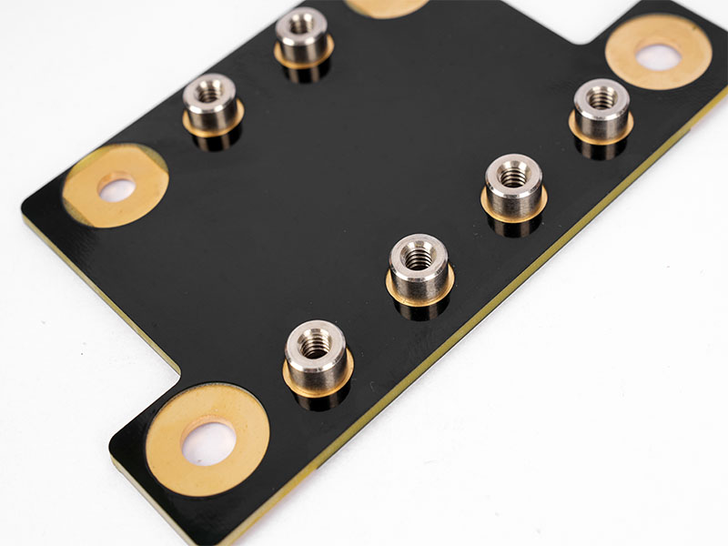
Double Sided PCB Assembly – Free DFM & Full Certified Component Sourcing
Double sided PCB assembly presents unique challenges, including precise dual-layer component placement, reliable soldering, and protecting delicate traces during the assembly process.
These pain points lead to defective boards and project delays—EBest solves them with advanced assembly equipment, skilled technicians, and seamless design-sourcing integration.
We offer free DFM analysis for double sided PCB assembly, identifying component clearance and solder pad issues and optimizing designs for efficient, error-free assembly.
Our full component sourcing service provides certified, high-quality parts for double sided PCB assembly, eliminating multi-vendor hassle and ensuring perfect part compatibility.
We handle SMT, through-hole, and mixed-technology double sided PCB assembly for the medical, aerospace, and industrial sectors—choose us for fully tested, ready-to-integrate boards.
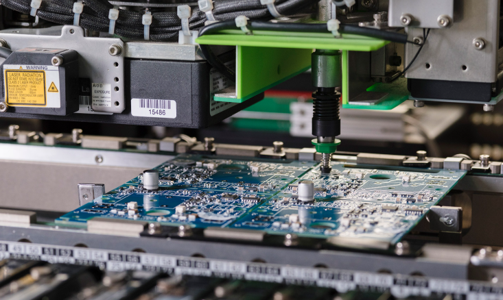
What Is EBest’s Step-by-Step Double Sided PCB Assembly Workflow?
- Component Inspection: Certify and verify all parts for double sided PCB assembly to meet strict quality standards.
- Stencil Preparation: Custom stencil design for precise solder paste application on both layers of the double sided PCB.
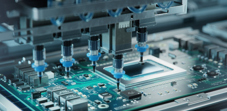
- SMT Placement: Automated high-precision SMT component placement on the top and bottom layers of the double sided PCB.
- Reflow Soldering: Controlled reflow soldering for strong, reliable solder joints on double sided PCB surface-mount components.
- Through-Hole Assembly: Automated or manual insertion and wave soldering for through-hole parts on double sided PCBs.
- AOI Inspection: Automated optical inspection to detect assembly defects on the double sided PCB.
- Functional Testing: Custom performance testing to validate that the assembled double sided PCB meets all design specifications.
What Industries & Applications Use Double Sided PCBs?
Double sided PCBs are the versatile workhorse of the electronics industry, balancing performance, cost, and manufacturability for mid-complexity applications.
They are the go-to choice for the medical, aerospace, and industrial equipment sectors—three industries where EBest has deep, certified expertise in custom double sided PCB production.
Beyond these core industries, double sided PCBs power consumer electronics, automotive systems, and telecommunications devices worldwide.
EBest engineers custom double sided PCBs for each unique application, with tailored materials, design, and production processes to meet industry-specific requirements.
EBest’s Double Sided PCB Case Studies – Medical, Aerospace, Industrial
- Medical: ISO 13485-certified double sided PCBs for portable ECG monitors—compact design, low power consumption, and high reliability for clinical use.
- Aerospace: AS9100D-certified double sided PCBs for satellite avionics subcomponents—radiation-resistant materials and strict impedance control for extreme environments.
- Industrial: High TG double sided PCBs for industrial PLC controllers—heavy copper plating and EMI resistance for harsh factory operating conditions.
Double Sided vs Single Sided PCB – Which Is Right For Your Project?
Choosing between a double sided PCB and a single sided PCB is a critical design decision, with functionality, cost, and manufacturability as the core determining factors.
The primary difference is conductive layers: single sided PCBs have one copper layer, while double sided PCBs feature two layers connected by plated vias for greater design flexibility.
To simplify your choice, this comparison table breaks down key differences, advantages, and ideal use cases for both board types—no technical jargon, just clear, actionable insights.
| Key Feature | Single Sided PCB | Double Sided PCB |
|---|---|---|
| Conductive Layers | 1 single copper layer | 2 copper layers (top/bottom) with plated vias |
| Component Density | Low – limited trace and part placement | High – dual-layer space for complex component layouts |
| Signal Routing | Basic – no complex trace paths possible | Flexible – complex routing with minimal crosstalk and EMI |
| Power Handling | Low – suitable only for basic low-power devices | Medium-High – ideal for industrial and medical high-power applications |
| Design Flexibility | Very limited – no layer switching capability | High – supports impedance control and RF/high-speed design |
| Ideal Use Cases | Toys, calculators, basic sensors | Medical devices, aerospace subcomponents, industrial controllers |
| Industry Certifications | Rarely required | Standard for medical, aerospace, and industrial applications |
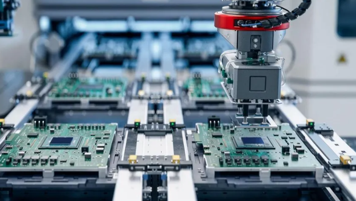
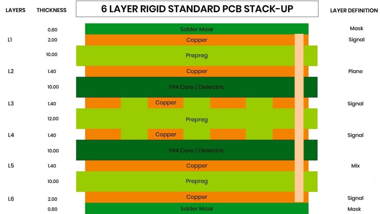
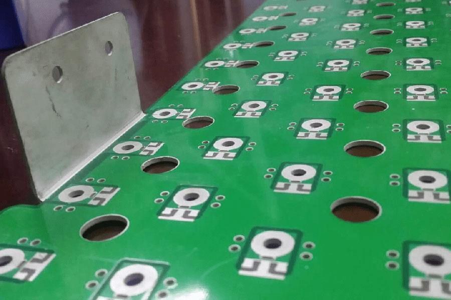
What Is The Step-by-Step Double Sided PCB Manufacturing Process?
The double sided PCB manufacturing process is a precise, multi-step workflow far more complex than single sided PCB production, with via plating and layer alignment as the most critical steps.
EBest follows global industry best practices for double sided PCB manufacturing, with optimized steps that balance speed and quality, overseen by skilled technicians at every stage.
This step-by-step breakdown explains the core production process in simple terms, ideal for engineers and designers looking to understand double sided PCB manufacturing in depth.
Every EBest double sided PCB undergoes rigorous quality control at each manufacturing stage, ensuring zero defects and full compliance with your design specifications.
Core Steps In Making a High-Quality Double Sided PCB
- Design File Validation: Optimize double sided PCB Gerber files with DFM analysis to ensure full manufacturability.
- Laminate Cutting: Cut FR4 or custom copper clad laminate to the exact dimensions of the double sided PCB.
- Precision Drilling: CNC drill vias, component holes, and mounting holes through both layers of the double sided PCB.
- Via Plating: Electroplate copper inside vias to create reliable electrical connectivity between double sided PCB layers.
- Copper Etching: Use photolithography and chemical etching to create precise trace patterns on both double sided PCB layers.
- Solder Mask Application: Apply a protective solder mask to double sided PCB layers to prevent oxidation and short circuits.
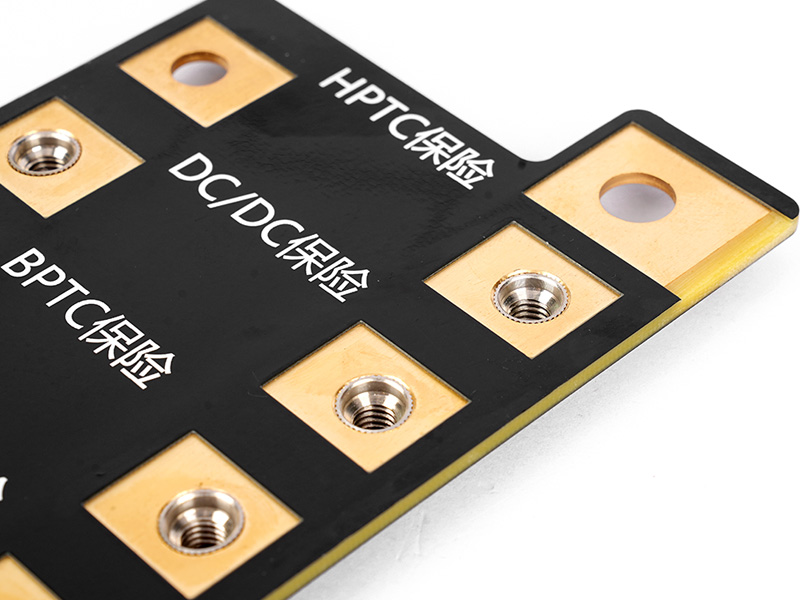
- Silkscreen Printing: Print component labels and logos on the double sided PCB for easy assembly and component identification.
- Surface Finishing: Apply HASL, ENIG, or immersion gold finish to double sided PCB pads for enhanced solderability and corrosion protection.
- Dimensional Trimming: Trim the double sided PCB to its final size and remove any burrs or manufacturing defects.
- Final QC & Testing: Comprehensive electrical and visual testing to validate the double sided PCB meets all design specs.
- Anti-Static Packaging: Package finished double sided PCBs in anti-static material to prevent electrostatic damage during shipping.
FAQ – Common Questions About Double Sided PCBs Answered
What is the best material for double sided PCB manufacturing?
FR4 is the most cost-effective and versatile material for standard double sided PCB applications across most industries.
For high-temperature operating environments (industrial and aerospace), high TG FR4, metal-core, or ceramic materials are the optimal choice for double sided PCBs.
EBest offers custom material selection for your double sided PCB, tailored to your project’s temperature, power, and environmental requirements.
Can double sided PCBs support high-speed and RF applications?
Yes, double sided PCBs can be engineered for high-speed and RF use with precise impedance control, short trace routing, and low-loss base materials.
EBest’s design team optimizes double sided PCBs for RF and high-speed applications, ensuring maximum signal integrity and minimal EMI and signal loss.
Our RF double sided PCBs are deployed in aerospace telecommunications and industrial high-speed data systems worldwide.
What is the typical turnaround time for double sided PCB production?
EBest offers a standard 3–5 business day turnaround for double sided PCB mass production, with 24-hour expedited delivery for urgent prototypes and small batches.
Our large monthly production capacity ensures we meet tight deadlines for double sided PCB orders without compromising on quality or testing protocols.
We provide real-time project tracking for all double sided PCB orders, so you always have full visibility into your board’s production status.
Does EBest offer custom sizes and shapes for double sided PCBs?
Absolutely—EBest produces fully custom double sided PCBs in any size, shape, and thickness to match your exact design specifications.
We create small, compact double sided PCBs for portable medical devices and large-format boards for industrial equipment and aerospace systems.
Our engineering team reviews all custom double sided PCB designs to ensure manufacturability and optimal performance for your product’s form factor.
Does EBest provide technical support for double sided PCB projects?
Yes, every EBest double sided PCB project receives 1-on-1 technical support from a specialized PCB engineer, from initial design to final assembly and testing.
Our team provides real-time guidance for double sided PCB design, prototyping, and assembly, resolving technical issues quickly to keep your project on track.
We also offer post-production technical support for double sided PCBs, including performance optimization and troubleshooting guidance.
Can EBest handle high-volume double sided PCB mass production?
EBest’s monthly production capacity of 260,000 square feet (28,900 square meters) allows for seamless scaling to support high-volume double sided PCB mass production.
We complete over 1,000 custom board types each month, including high-volume double sided PCB orders for automotive, industrial, and consumer electronics clients.
Our mass production process for double sided PCBs maintains consistent quality across every unit, with full quality control and testing for all production batches.
Order Your Custom Double Sided PCB From EBest Today
EBest is a global leader in double sided PCB manufacturing, with 20+ years of specialized expertise in custom design, rapid prototyping, and professional assembly.
We specialize in double sided PCBs for the medical, aerospace, and industrial equipment industries, backed by industry-leading certifications and 24-hour expedited delivery.
Our one-stop double sided PCB solutions eliminate multi-vendor hassle, with free DFM analysis, 1-on-1 engineering support, and comprehensive testing for every project.
Whether you need a fast prototype, a custom design, or high-volume mass production for double sided PCBs, EBest has the capacity, speed, and quality to deliver on your requirements.
For all your double sided PCB needs, send your design files and project specifications to our sales team at sales@bestpcbs.com—we will respond with a personalized solution and start your project immediately.