How Can Some Inductors be Active and Others Passive? An inductor is traditionally viewed as a passive part that stores energy in a magnetic field. Yet engineers often encounter the term “active inductor” in RF design, analog circuits, and integrated systems. This raises a natural question: how can an inductor be both passive and active?
The answer lies in understanding the physical nature of real inductors and how active circuits replicate inductive behavior using transistors. Both serve important roles, but for very different reasons.
What Defines a Passive vs Active Component?
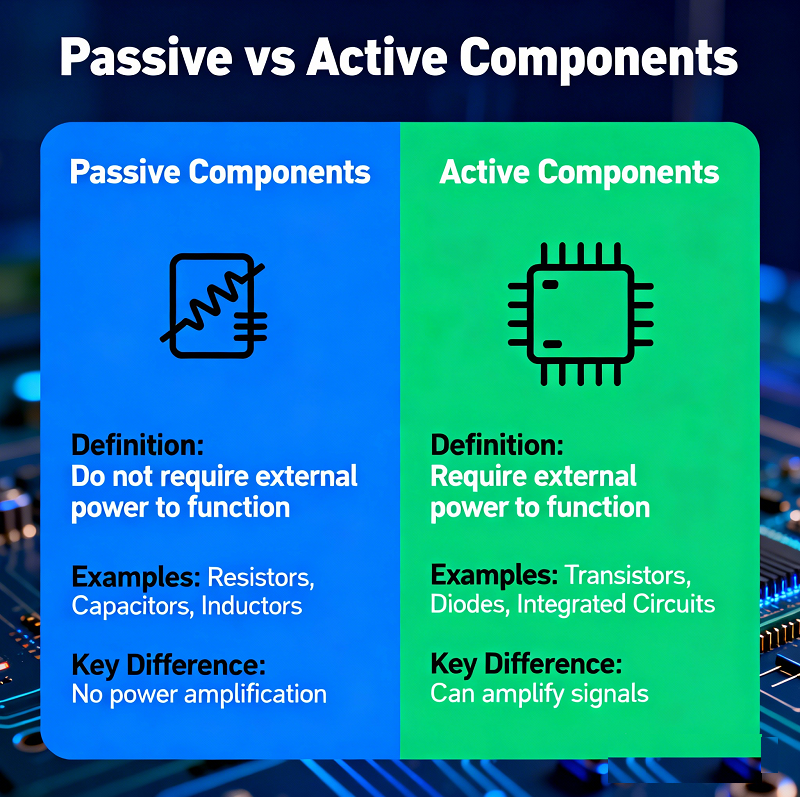
A passive component does not generate or amplify energy. It reacts directly to the applied electrical stimulus and cannot increase a signal’s power. Examples include resistors, capacitors, and classical inductors. They contribute predictable impedance but do not require an external power rail.
Active components, such as transistors, op-amps, and ICs, control current flow and may provide amplification or buffering. They need supply voltage and can introduce gain, shaping the signal beyond what passive parts can offer.
Understanding this boundary clarifies the discussion: a real inductor made from a coil is always passive. A circuit that imitates an inductor using active devices can appear inductive, but it is not passive. If you want to know more about active vs passive components, you can read our another post: Key differences between active and passive components
Are Inductors Active or Passive?
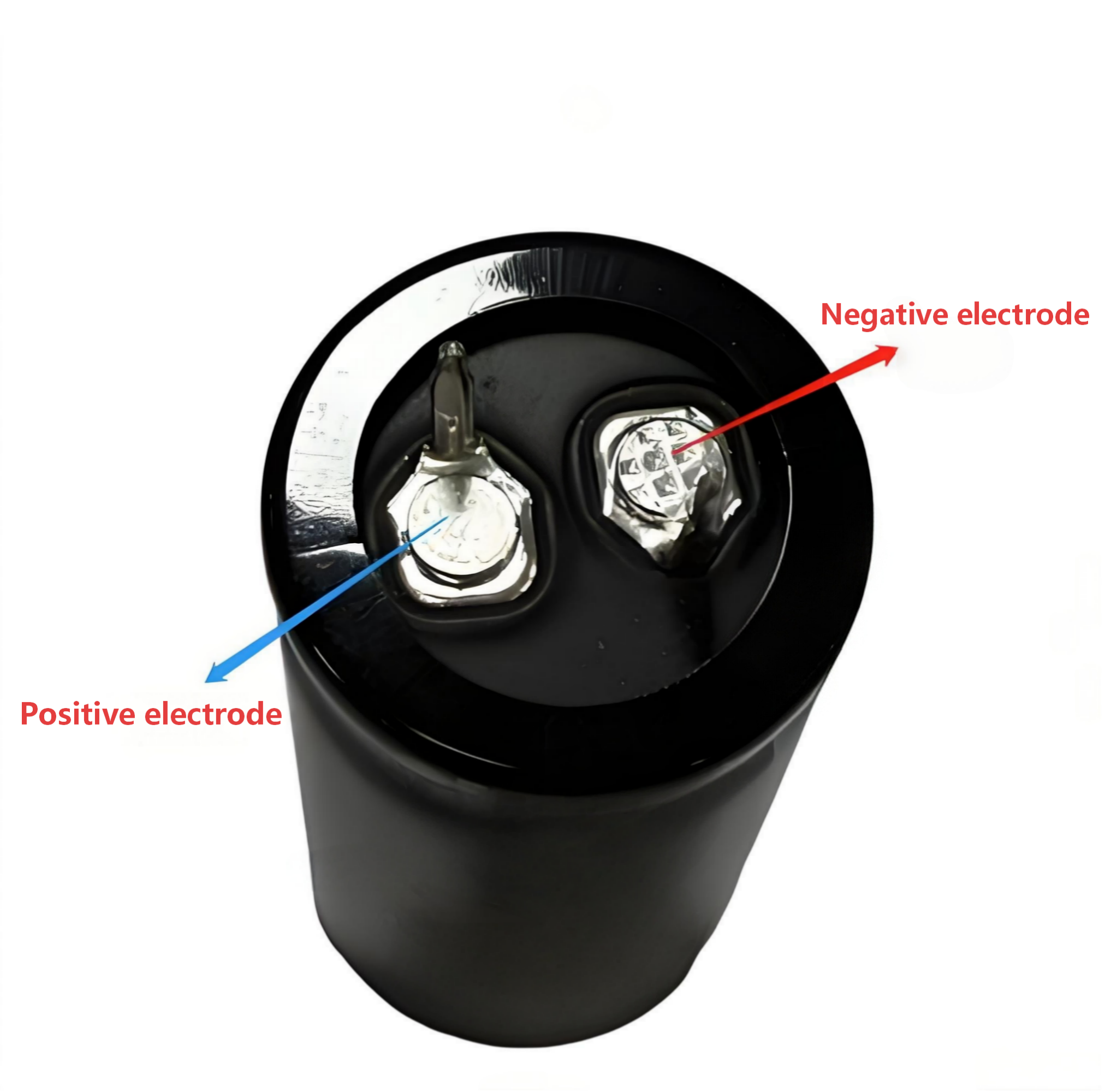
Inductors are passive components. A real inductor does not need an external power supply and cannot amplify signals—it simply stores energy in a magnetic field when current passes through it. Because it neither generates nor controls power using another energy source, it is classified as a passive device in electronics.
However, in modern RF and integrated circuit design, you may encounter the term active inductor, which can cause confusion. These are not physical coils but transistor-based circuits that imitate the behavior of an inductor. Since they require external power and use active devices like MOSFETs or BJTs to create inductive reactance, they are considered “active.” So while true inductors are always passive, engineers sometimes build circuits that behave like inductors using active components.
Why Inductors Are Classified as Passive Components?
The behavior of a physical inductor is rooted in fundamental electromagnetic principles. When current flows through a coil, a magnetic field forms. As the current changes, the magnetic field changes, resisting that shift. This energy exchange happens without any external power source.
A real inductor is therefore passive because:
- It can store energy but does not create energy.
- It influences current change without external power.
- It cannot add gain to any signal path.
- It operates based solely on electromagnetic induction.
Even in complex designs such as buck converters or class-D amplifiers, the inductor simply reacts to switch transitions and waveform shapes created by active devices. All “dynamic” behavior is still passive in nature.
How Does an Inductor Act at T 0+ and T ∞?
At T = 0⁺, an inductor behaves like a short-term open circuit because it resists any sudden change in current. The moment a voltage is applied, the current through the inductor starts at zero and increases gradually, so the inductor initially blocks current flow as if it were an open switch.
At T = ∞, an inductor behaves like a short circuit because once the current reaches a steady state, the inductor no longer opposes it. The stored magnetic field becomes constant, the inductor’s voltage drops to zero, and it effectively acts as a piece of wire with minimal resistance.
Why Some Inductors Appear “Active” in Switching Power Circuits?
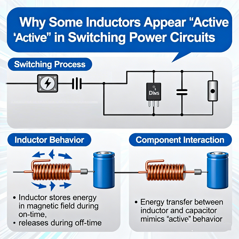
In switching circuits, an inductor often behaves in a way that looks purposeful and controlled—almost like an active element. For example:
- In a buck converter, the inductor ramps current up and down in sync with the MOSFET switching.
- In a boost converter, the inductor releases stored energy to lift the voltage.
- In a flyback design, the inductor (transformer primary) delivers energy during off-time.
This controlled energy delivery can seem active. But the inductor remains passive because:
- It performs no amplification.
- It has no supply pins.
- All action results from controlled switching around it.
The inductor is only following physics. Its “active-looking” behavior is driven by the switching controller, not the inductor itself.
How Active Inductors Work?
Active inductors exist because integrated circuits cannot easily include large, high-quality coils. Instead, designers use transistors and feedback networks to replicate inductive reactance.
Common active inductor approaches:
- Gyrator circuits: Create an inductive response using a capacitor and an active device.
- MOSFET-based inductors: Leverage transconductance to shape current like a coil would.
- Gm-C active filters: Combine tunable transconductance with capacitors for high-frequency inductive behavior.
Active inductors rely on:
- Bias current
- Voltage gain
- Feedback loops
These elements allow the circuit to emulate inductance over a chosen frequency range. They do not store energy magnetically; instead, they reproduce the impedance profile of an inductor electrically.
How to Tell Whether an Inductor Is Passive or “Active-Like”?
The simplest way is to examine its structure or schematic.
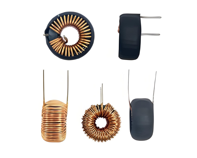
A passive inductor:
- Contains a coil of copper wire.
- May use ferrite, iron, or air as the core.
- Has no power supply pins.
- Always presents inductive reactance at AC.
- Stores energy in a real magnetic field.
An active inductor:
- Includes MOSFETs, BJTs, resistors, and capacitors.
- Requires biasing from VCC or VDD.
- Does not behave like an inductor at DC.
- Mimics inductance only across a designed range.
- Does not produce a true magnetic field.
If it physically coils wire, it is passive. If it needs biasing, it is active.
Why Use Active Inductors Instead of Passive Ones?
Engineers select active inductors for reasons tied to integration, size, and flexibility. A real inductor may be too large, too costly, or incompatible with an integrated CMOS flow. Active versions offer:
- Very small footprint for RF ICs and SoCs.
- Electronically adjustable inductance for tunable filters.
- Higher effective inductance than what is possible in a small coil.
- Better integration on silicon with no magnetics required.
- Lower parasitics compared with some wound inductors.
This makes active inductors popular in:
- RF front-ends
- On-chip matching networks
- Integrated oscillators
- Bluetooth, Wi-Fi, and mmWave circuits
- Adaptive analog systems
Why Passive Inductors Are Still Needed?
Although active inductors are flexible, they cannot replace wound inductors when real magnetic energy storage or high linearity is required. Passive inductors excel in:
- Energy transfer systems
- Power converters
- High-current paths
- EMI suppression
- Resonant circuits with high Q
- Audio crossover networks
- RF circuits where low noise is important
Passive inductors also work over a broad frequency range and do not rely on bias currents. They withstand much higher power levels than active circuits.
When Should You Use a Passive Inductor?
A passive inductor is the correct choice when the application needs real, physical energy handling. Use one when the design involves:
- Power conversion
- DC-DC regulation
- Motor control circuits
- High-current feeding
- RF filters needing high Q
- Low-noise front-end requirements
When reliability, linearity, and energy efficiency matter, a real inductor is essential.
When Should You Use an Active Inductor?
Active inductors become practical when design priorities shift:
- The circuit must be fully integrated on a chip.
- Board space is extremely limited.
- Tunability is required through voltage or current adjustments.
- Only small-signal behavior matters, not high power.
- The circuit’s operating band is narrow, such as RF.
If the goal is impedance shaping, not energy transport, an active inductor offers a compact and configurable solution.
Conclusion
A traditional inductor with a wire coil is always passive. It stores energy in a magnetic field and cannot amplify signals. Active inductors, on the other hand, are transistor-based circuits that imitate inductive behavior using gain and feedback. They are “active” because they need power and introduce controlled impedance rather than storing energy.
Both types play important roles in electronics. Understanding their differences helps engineers select the right component for RF filters, switching regulators, mixed-signal ICs, and miniaturized platforms where performance, size, and frequency all shape design strategy.