PCB manufacturing PCB manufacturing
Home > Blog

high density interconnect pcb

HDI PCBs – High Density Interconnect PCB Manufacturer
Saturday, February 28th, 2026

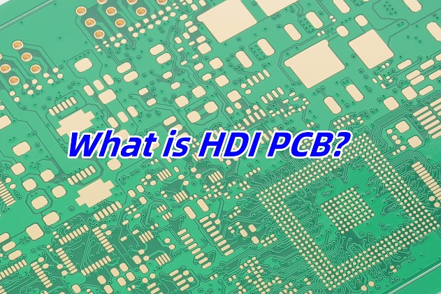
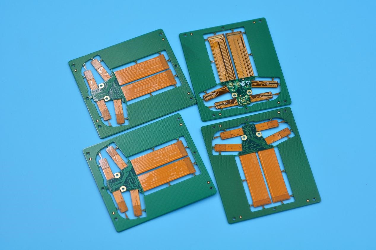
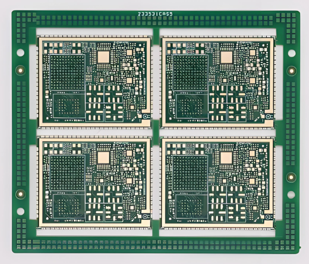
What Is a High Density Interconnect PCB?

High Density Interconnect PCB refers to a multilayer structure that uses laser microvias, thin dielectric layers, and sequential lamination to increase routing density and improve electrical performance. Instead of routing signals through long mechanical vias, HDI stackup design focuses on short vertical transitions between adjacent layers. This reduces inductance, improves impedance control, and allows fine-pitch BGA escape without increasing board size.

Typical HDI electrical parameters used in engineering documentation include:

  • Line width / spacing: 60–75 µm (advanced builds may reach 40 µm)
  • Microvia finished hole: 75–100 µm
  • Dielectric thickness between HDI layers: 40–80 µm
  • Copper thickness: 12–18 µm outer HDI layers, 18–35 µm inner layers

HDI stackup design emphasizes signal-reference plane proximity. Short dielectric spacing lowers loop inductance and stabilizes return paths, which becomes critical in AI server and high-speed computing boards.

HDI PCBs - High Density Interconnect PCB Manufacturer

High Density Interconnect PCB

When Should You Choose an HDI PCB Instead of a Standard Multilayer PCB for AI Server or High-Speed Systems?

HDI becomes necessary when routing density or electrical requirements exceed conventional PCB capability. AI server motherboards, accelerator modules, and edge computing boards frequently adopt HDI because processor pin counts and high-speed channels increase dramatically.

Engineering decision indicators:

  • BGA pitch ≤ 0.5 mm
  • High-speed links above 10–25 Gbps
  • Large processor or FPGA packages exceeding 1000 pins
  • Board size constraints requiring compact layouts
  • Power delivery networks needing dense decoupling arrays

In AI server designs, HDI reduces via stubs and shortens differential pair transitions. This helps maintain insertion loss budgets and improves eye-diagram margins during high-frequency operation.

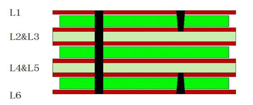
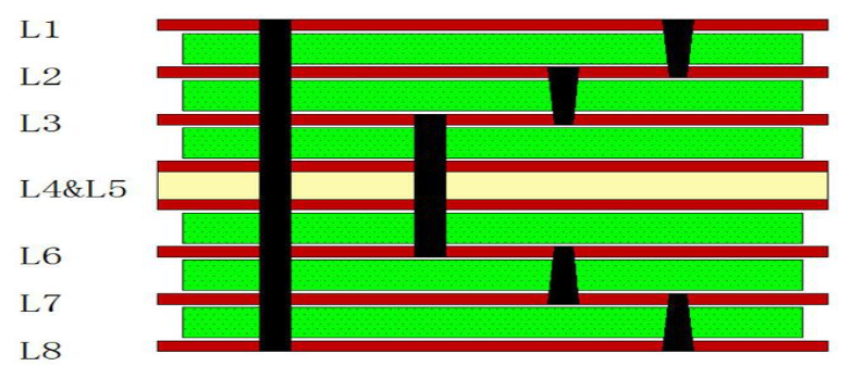
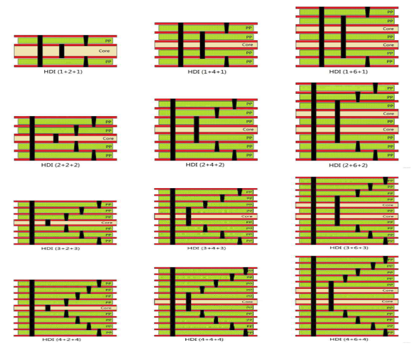
How Do 1+N+1 and 2+N+2 HDI Stackup Design Strategies Affect Routing Density and Manufacturing Risk?

HDI Stackup Design Comparison Table

Stackup TypeTypical Microvia DepthRouting DensityLamination CyclesApplication Example
1+N+1L1-L2 / L(n-1)-LnMedium2 cyclesRobotics controllers, embedded CPU boards
2+N+2L1-L2-L3 stacksHigh4 cyclesAI server compute modules
3+N+3Multi-stack microviasVery High6+ cyclesAdvanced telecom or HPC

More build-up layers increase routing flexibility but also introduce additional lamination cycles. Engineers often begin with 1+N+1 and evaluate whether further build-up layers are required based on BGA escape results.

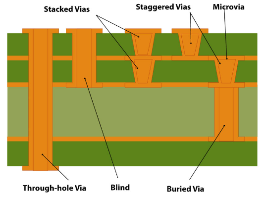
HDI Microvia Engineering Parameter Table

ParameterRecommended RangeEngineering Impact
Laser Via Diameter75–100 µmRouting density and plating reliability
Capture Pad Size150–250 µmAnnular ring control
Aspect Ratio≤ 0.8:1Prevents plating voids
Via StructureStaggered preferredImproves thermal reliability
Copper Fill Thickness15–25 µm capRequired for via-in-pad

Microvia planning should begin during stackup definition because changing via structure later can require redesigning large portions of the layout.

When Does Via-in-Pad Become Mandatory in Fine-Pitch HDI PCB and AI Server BGA Fanout?

Via-in-pad is used when routing channels around BGA pads are insufficient. In AI server processors or high-density networking ASICs, pad pitch often forces vertical signal escape.

Engineering scenarios where VIP is justified:

  • 0.4 mm pitch GPU or AI accelerator packages
  • High-speed differential pairs requiring shortest path
  • Dense decoupling networks under core voltage rails

VIP pads require copper filled microvias, planarization to maintain flatness, and careful solder mask design.

How Does HDI PCB Compare to Standard PCB in Signal Integrity, Size Reduction, and Layer Utilization?

Engineering MetricHDI PCBStandard PCB
Via Stub LengthVery ShortLong unless backdrilled
Routing Channel DensityHighLimited
Loop InductanceLowerHigher
Board AreaReducedLarger
Layer EfficiencyHigh utilizationLower utilization
EMI PerformanceImproved due to compact loopsDepends on layout strategy

Shorter vertical transitions in HDI improve signal eye margin in high-frequency environments such as AI servers.

What Is the Real HDI Fabrication Flow and Which Process Steps Affect Yield Most?

HDI Fabrication Process Table

StepKey Parameter ControlRisk Area
Core LaminationThickness tolerance ±10 µmWarpage
Build-Up LaminationResin flow uniformityVoid formation
Laser DrillingPosition accuracy ±20 µmVia misalignment
Copper PlatingCurrent density controlMicrovia reliability
Imaging & EtchLine width tolerance ±10 µmSignal impedance shift

Microvia plating uniformity and dielectric thickness control are major contributors to HDI manufacturing yield.

Which Materials Are Preferred for HDI Stackup Design in AI Server PCB and High-Speed Applications?

Material CategoryDk RangeDf RangeTypical Use
High Tg FR-43.8–4.20.015–0.018General HDI boards
Low Loss Laminate3.2–3.60.004–0.009AI server and networking
RCC Thin Dielectric~3.50.01Build-up layers

Material selection should align with both electrical performance targets and thermal cycling conditions during assembly.

How Do Engineers Route Fine-Pitch BGA on HDI PCB Without Signal Integrity Problems or Rework Risk?

Routing strategy begins with stackup planning rather than trace drawing. Engineers typically follow a structured workflow:

  1. Assign ground reference layers adjacent to signal layers
  2. Escape first BGA rows using microvias to inner routing layers
  3. Maintain differential pair spacing within controlled tolerance
  4. Avoid excessive layer transitions that introduce impedance discontinuities

Typical HDI differential routing parameters used in AI server layouts:

  • Pair spacing: 100–150 µm
  • Trace width: 65–80 µm
  • Reference plane spacing: 60 µm

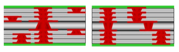
How Can You Improve HDI PCB Reliability Against CAF, Microvia Fatigue, and Warpage?

Failure MechanismRoot Cause  Engineering Control
CAF GrowthMoisture + voltage biasIncrease conductor spacing
Microvia FatigueCTE mismatchUse staggered microvias
WarpageCopper imbalanceSymmetrical copper distribution

Balanced copper distribution across layers significantly improves long-term reliability in high-power computing environments.

What Drives HDI PCB Cost and How Does a Detailed HDI Cost Breakdown Help Engineering Decisions?

HDI Cost Breakdown Engineering Table

Cost DriverProcess ImpactCost Influence
Sequential LaminationAdditional build-up layersHigh
Laser Microvia DrillingEquipment timeMedium-High
Copper Filled VIPExtra plating stepsMedium
Fine Line ImagingTight tolerance controlMedium
Low Loss MaterialMaterial premiumVariable

Understanding HDI cost breakdown allows engineers to optimize stackup design early and avoid unnecessary process steps.

Why Choose EBest as Your High Density Interconnect PCB Manufacturer?

If you are moving into HDI PCB projects, your biggest risk is not the CAD work. It is misalignment between design intent and fabrication reality. EBest Circuit positions itself as a one-stop PCBA service provider that better understands the needs of engineers, so your stackup, microvias, and assembly choices stay consistent from quote to shipment.

  • Free DFM and process adaptation suggestions before release
  • 20 years serving 1800+ customers and 10,000+ engineers
  • One-Stop Service: PCB, components, PCBA, testing, and box-building
  • No MOQ with personal service for prototypes and small batches
  • ISO9001/ISO13485, IATF16949, AS9100D quality systems support
  • MES & traceability for process tracking and accountability
  • 1.5-week rapid PCBA delivery options for urgent programs
  • Technical support before and after sales, with prompt feedback (often within 12 hours)
  • Prototype & small volume welcome, with quick turn-out and on-time delivery focus
  • High quality builds, special requests available, supported by a strong R&D team

FAQs

1. What BGA pitch usually requires HDI stackup design?

HDI stackup design is commonly selected when BGA pitch approaches 0.5 mm because routing density becomes constrained using only mechanical vias.

2. Is 2+N+2 always required for AI server HDI PCB?

Many AI server boards begin with 1+N+1 structures and only move to 2+N+2 when routing density requires additional build-up layers.

3. Are stacked microvias reliable for high-power systems?

Stacked microvias can be reliable when copper filling and plating thickness are well controlled, though staggered structures often improve durability.

4. Does HDI PCB always reduce total layer count?

HDI improves routing efficiency and signal integrity but does not always reduce total layer count.

5. How early should HDI stackup design be finalized?

Stackup definition should occur before placement and routing to prevent redesign cycles.

High Density Interconnect PCB: Everything You Should Know
Friday, September 27th, 2024

What is High Density Interconnect PCB?

High density Interconnect (HDI) PCB is a printed circuit board designed to meet the growing needs of modern electronic products. It allows for higher component density due to the use of thinner lines, smaller through-holes, and precise component placement. These boards are particularly popular in industries where miniaturization is key, such as smartphones, medical devices, and military equipment.

The HDI board uses the micro-blind hole technology to realize the circuit board design with high line distribution density, which is especially suitable for applications requiring high performance and high reliability. Compared with traditional PCBs, HDI boards have significant advantages in terms of volume, weight, wiring density and electrical performance, which can meet the electrical requirements of high-speed signals, provide impedance control of alternating current characteristics, high-frequency transmission capacity and reduce unnecessary radiation (EMI).

HDI PCBs use a combination of advanced technologies such as laser drilling and sequential lamination to enable denser wiring without compromising performance. By integrating smaller, more efficient through-holes, HDI boards offer greater functionality on a smaller footprint than traditional PCBs.

What is the Difference Between Connect and Interconnect?

The terms “connect” and “interconnect” may seem similar but serve distinct functions in electronics. “Connect” typically refers to the linking of two points, components, or circuits. This could be as simple as joining a wire to a terminal.

On the other hand, “interconnect” deals with more complex connections, usually involving the linking of multiple circuits or components within a system. In the context of HDI PCBs, interconnectivity is crucial because it defines how different layers and components of the board communicate. HDI technology optimizes these interconnections to make the board more efficient in terms of space and performance.

What is HDI PCB Stackup?

The stackup in HDI PCBs refers to how the multiple layers of the board are arranged. Stackups are critical in determining the board’s performance, particularly when it comes to signal integrity, power delivery, and heat dissipation. HDI stackups often involve intricate configurations that vary depending on the design’s complexity and purpose. Here are the most common types:

HDI PCB (1+N+1)

This is one of the simplest forms of HDI stackups, where “1+N+1” means there are two layers of high-density interconnect (one on each side) sandwiching N layers of traditional PCB. This structure is often used in applications where moderate complexity is required, providing a balance between performance and cost.

HDI PCB (2+N+2)

In this configuration, there are two HDI layers on each side of the N traditional layers. This setup allows for greater flexibility in routing, especially for complex designs requiring more components. The additional HDI layers enhance the board’s ability to manage signal transmission efficiently, making it suitable for high-performance applications.

ELIC (Every Layer Interconnection): Most Complex HDI

ELIC takes HDI technology to the next level. In this configuration, every layer of the PCB can interconnect directly with any other layer. This is the most advanced form of HDI stackup, offering unparalleled design flexibility and performance. However, it is also the most complex and expensive option. ELIC is often used in cutting-edge technology applications such as aerospace and military equipment.

Other HDI Stackups

What are the Advantages of HDI PCB?

The main advantage of the HDI board is its high-density interconnect design, through the use of micro lines and highly compact layout, can achieve higher interconnection density, thereby accommodating more electronic components in a limited space, improving the performance and function of the board. This design makes HDI boards particularly suitable for applications requiring high performance and high functional density, such as high performance computing, data centers, and mobile communication equipment, to support high-speed data transmission and processing.

The design of the HDI board also focuses on improving the anti-interference ability and reliability of the circuit board, by using better signal integrity and power management technology, effectively reduce the impact of electromagnetic interference and power noise on the circuit.

However, HDI boards also have some limitations. First of all, compared with other advanced boards, the cost of HDI boards is usually lower, because HDI manufacturing technology helps to use advanced packaging technology, but its processing is more difficult, higher requirements for technology and equipment, which may increase a certain cost. In addition, the material choice of HDI board will also affect its performance and cost, such as FR4, PI and BT materials have advantages and disadvantages, need to be weighed according to the specific application needs.

5 Types of Vias in HDI PCB

HDI PCBs rely on several types of vias to achieve their high-density interconnections. Each type of via has its specific role in the design and manufacturing process.

Blind Vias

Blind vias connect an outer layer of the PCB to one or more inner layers but do not extend through the entire board. These vias allow for complex routing without using unnecessary space on the PCB’s inner layers.

Buried Vias

Buried vias are located entirely within the board, connecting internal layers without appearing on the outer surfaces. This is ideal for designs where surface area needs to be preserved for components, while still allowing inter-layer connectivity.

Microvias

Microvias are tiny vias, typically created using laser drilling, that connect adjacent layers of the PCB. These are essential for HDI designs as they save space while maintaining high-density connections. They can be used in stacked or staggered configurations to optimize space and signal flow.

Staggered Vias

Staggered vias are microvias that are offset from each other across layers. This design allows for more flexibility in routing and avoids overlapping, making it a popular choice for HDI PCBs that require complex routing.

Through Hole Vias

Though not exclusive to HDI designs, through-hole vias extend through the entire PCB, connecting all layers. While these vias occupy more space, they are sometimes necessary for power connections or when working with thicker boards.

What is the Difference Between PCB and HDI PCB?

The key difference between a traditional PCB and an HDI PCB lies in the design and manufacturing process. Traditional PCBs use through-hole technology and thicker traces, limiting the board’s ability to accommodate high-density components. HDI PCBs, by contrast, use finer lines, smaller vias, and advanced interconnect techniques to maximize component density. Here are some key differences between them:

Manufacturing Processes

The embedded via and blind via technologies used in the manufacturing process of HDI (High-Density Interconnect) boards allow for the addition of more layers without increasing the thickness of the board, thereby improving space utilization. In contrast, the drilling process for standard PCBs is relatively simple, but as the number of layers increases, the board thickness also increases accordingly. This difference means that HDI boards require more advanced equipment and higher technical requirements during production.

Space Constraints

In space-constrained devices, such as smartphones and portable electronics, HDI boards are the ideal choice because they can integrate more functions within a smaller size. HDI boards can achieve a line width of 2/2 mil and a 10-layer board thickness of below 0.8mm. Standard PCBs, due to their larger size and lower integration, may not be suitable for these applications. The line width and spacing of regular PCBs are generally limited to 3/3 mil, and their thickness also has certain restrictions.

Performance Requirements

For high-end electronic products that require high-speed signal processing and complex circuit designs, HDI boards offer better performance. Due to their high density and efficiency, HDI boards can meet the high-performance demands of modern electronic devices. Standard PCBs, on the other hand, may not be suitable for these applications because of their lower signal transmission quality and higher latency.

Different Layering Methods

HDI boards are created through continuous stacking and lamination, resulting in advantages such as being “light, thin, short, and small.” Electrical interconnections between layers are achieved through conductive vias, embedded vias, and blind vias, making the structure different from standard multilayer boards. Most HDI boards are laminated two or more times (except for special structures), while standard boards are typically laminated once.

PTH vs. HDI PCB

Plated Through Hole (PTH) technology is commonly used in traditional PCBs and involves drilling holes through the entire board to connect different layers. This method, while reliable, is limited in terms of design flexibility and component density.

HDI PCBs, on the other hand, use smaller vias such as microvias, blind vias, and buried vias. These allow for more efficient use of space, making HDI technology the go-to solution for high-density, multi-layer designs.

High Density Interconnect PCB Applications

  • Communication equipment
  • Computers and servers
  • Automotive electronics
  • Medical equipment
  • Industrial control equipment
  • Consumer electronics
  • ADAS system
  • Wireless connection module

For nearly 20 years, EBest Circuit (Best Technology) have always been committed to providing overseas customers High Mixed, Low Volume products with Reliable Quality and Quick Delivery, and are determined to become one of most trusted partners in the field of printed circuit boards and PCBA. As an expert of HDI PCB manufacturer, we are so confident that we can provide the highest quality product that highly meet your specifications.