PCB manufacturing PCB manufacturing
Home > Blog

heavy copper pcb

Thick Copper PCB Design, Prototype & Assembly | Fast Custom Solutions for Medical, Aerospace & Industrial (2026 Expert Guide)
Thursday, February 26th, 2026

Why EBest Is the #1 Choice for Your Thick Copper PCB Manufacturing (Proven for Medical/Aerospace/Industrial)

When it comes to thick copper PCB manufacturing—whether you need precise design, rapid prototyping, or reliable assembly—EBest is your first and best choice. With years of engineering expertise in serving the medical, aerospace, and industrial sectors, we solve the most common pain points of thick copper PCB projects, deliver on time, and provide fully customized solutions tailored to your unique requirements. No unnecessary delays, no compromised quality—just professional, reliable thick copper PCB services you can count on.
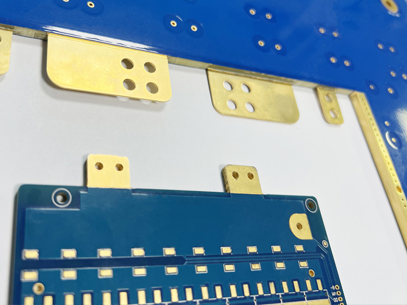
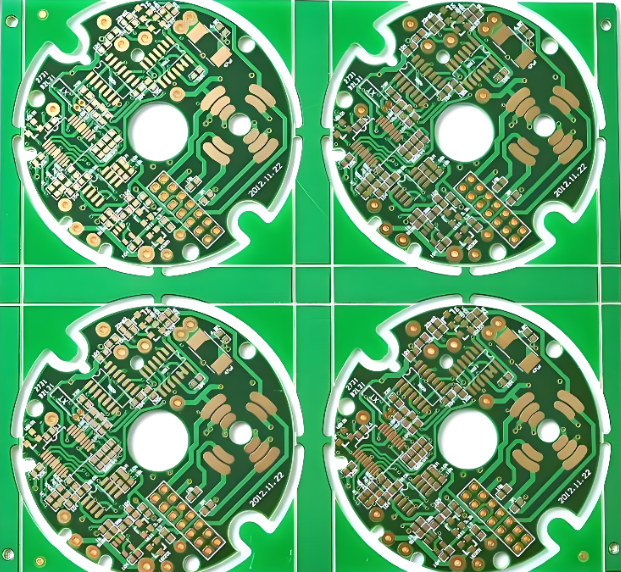
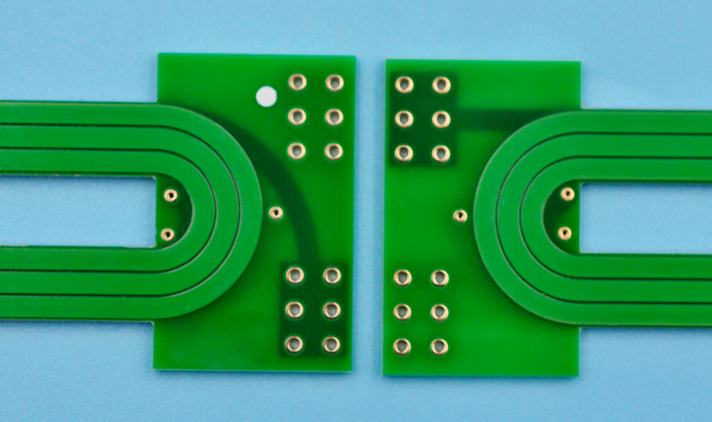
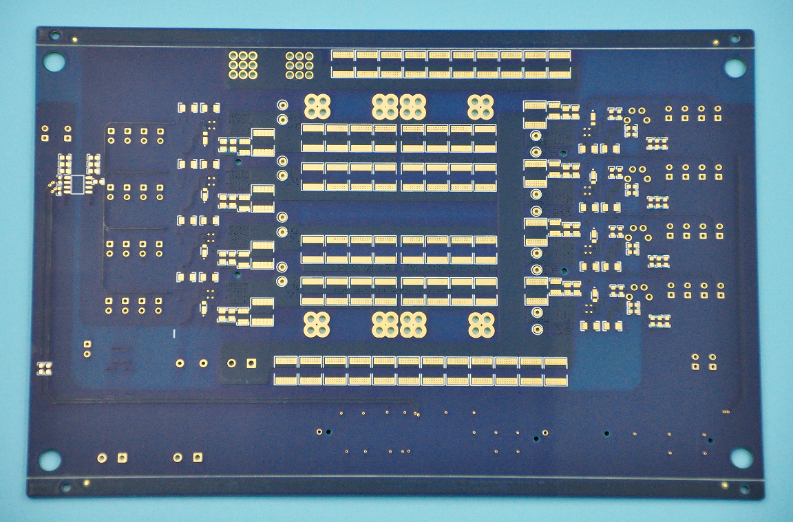
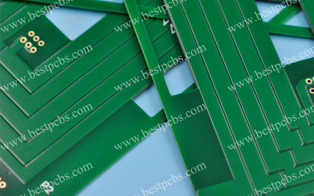
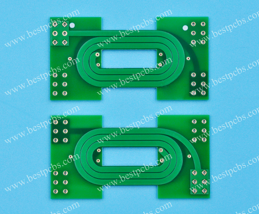
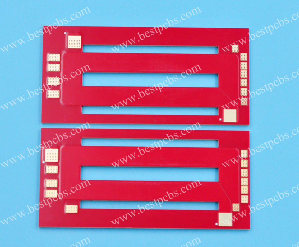
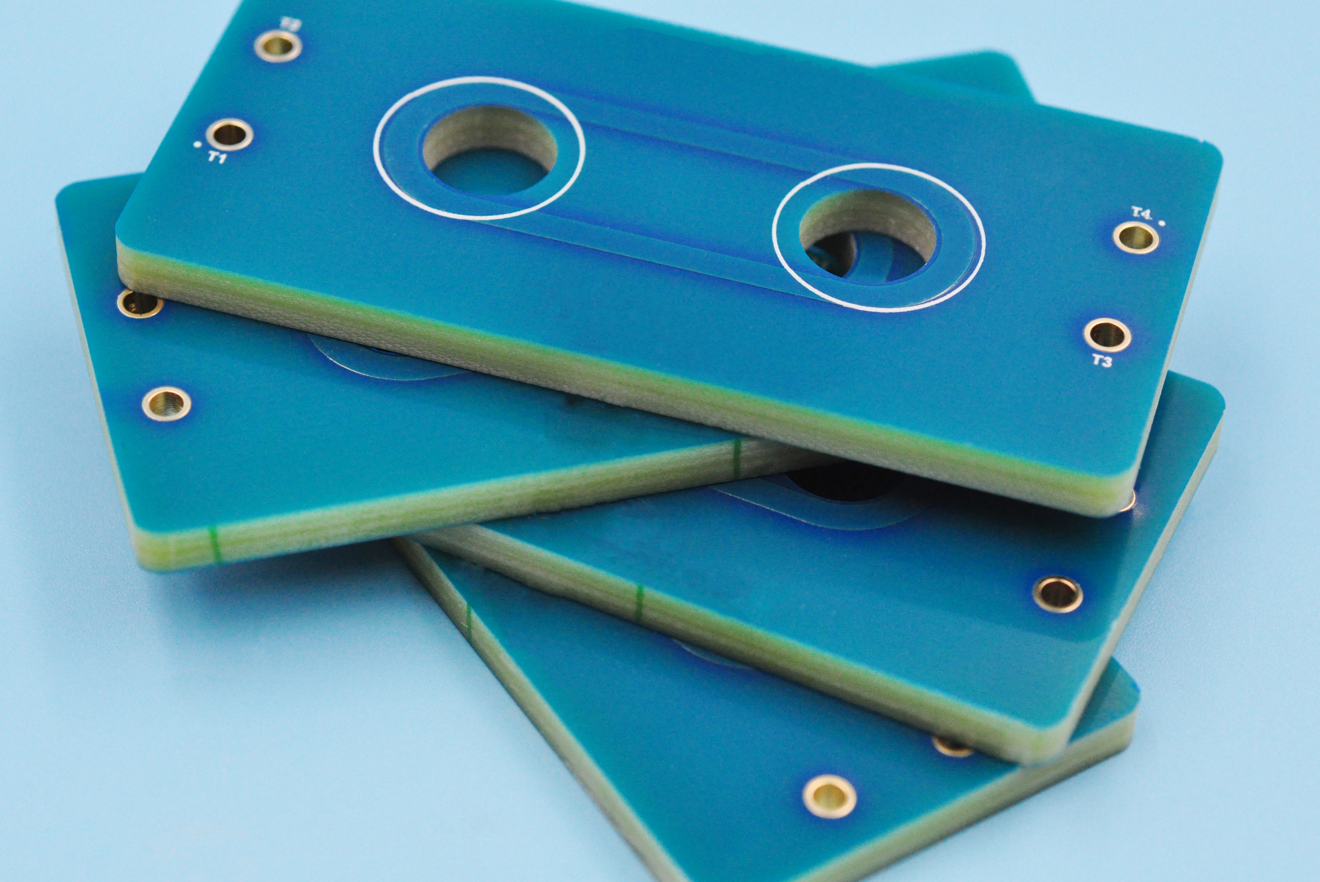
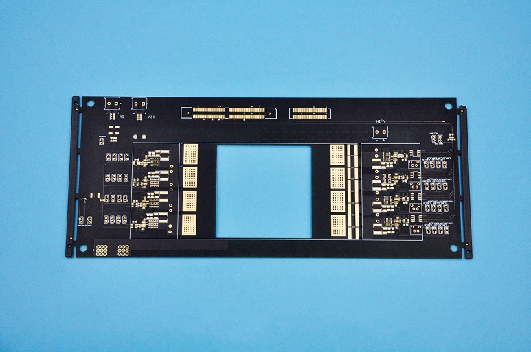
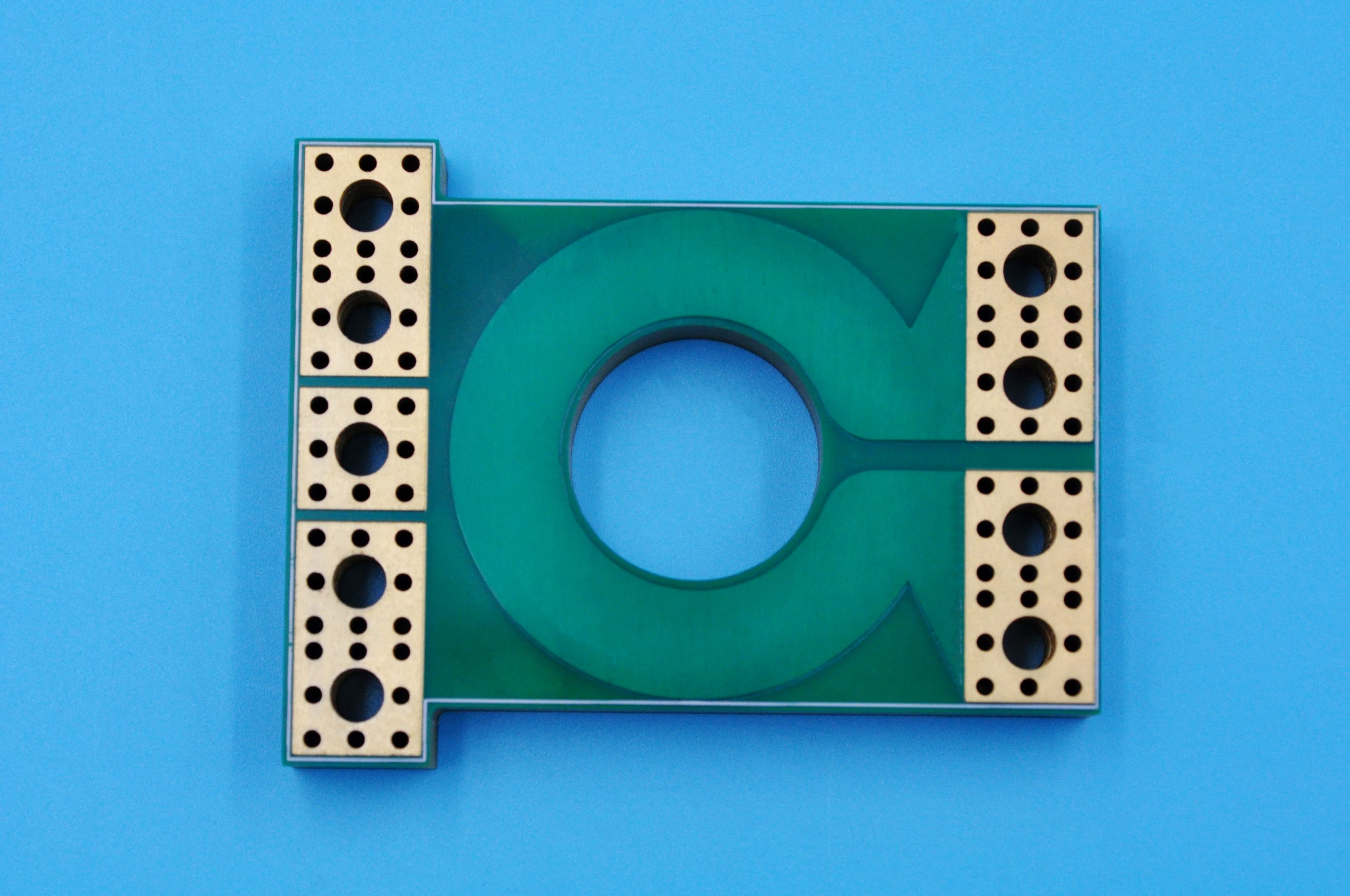
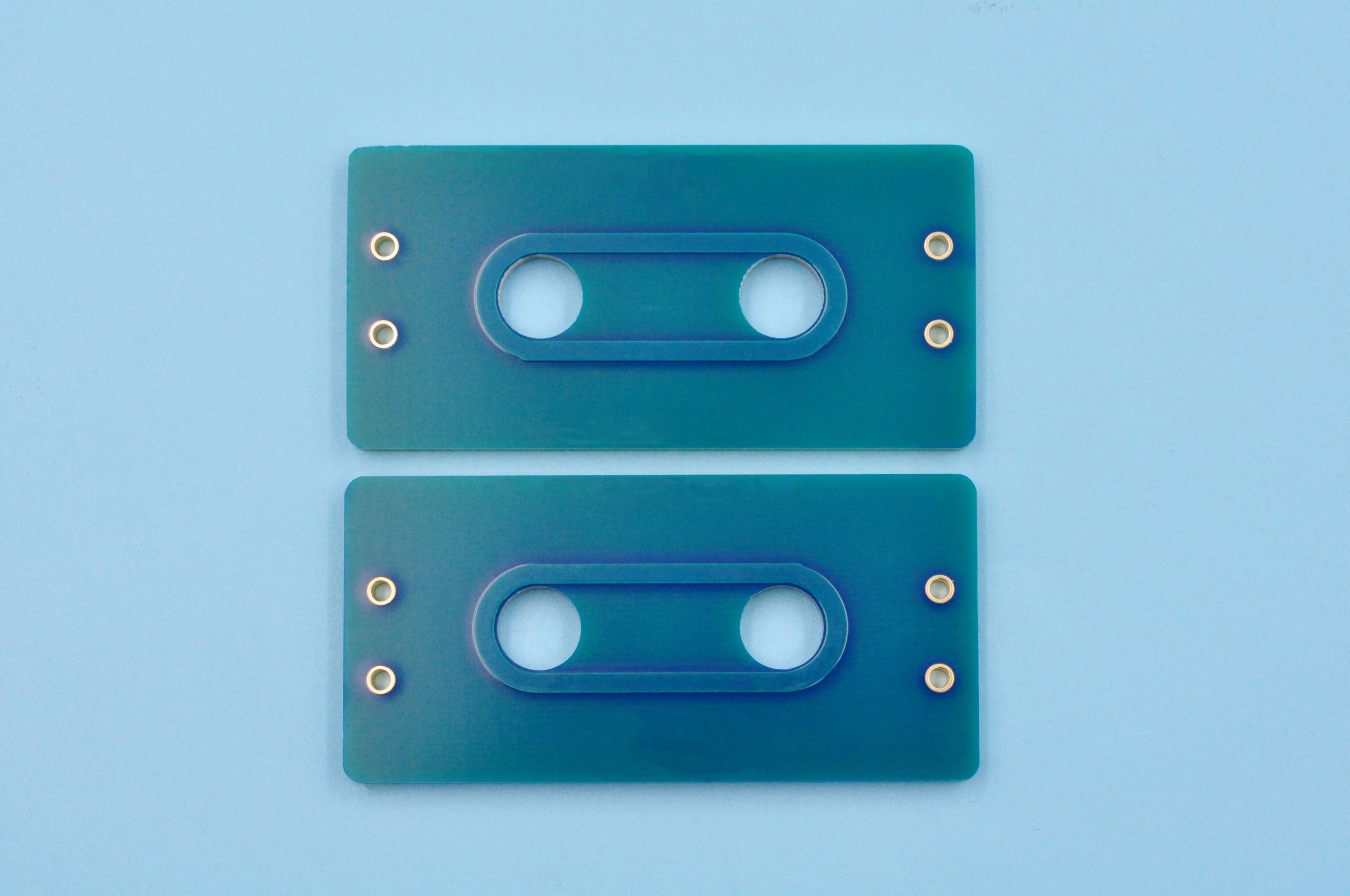
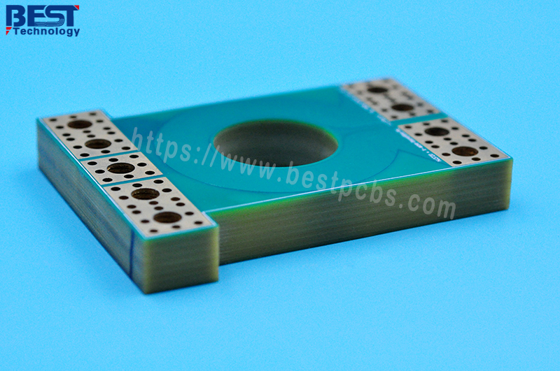
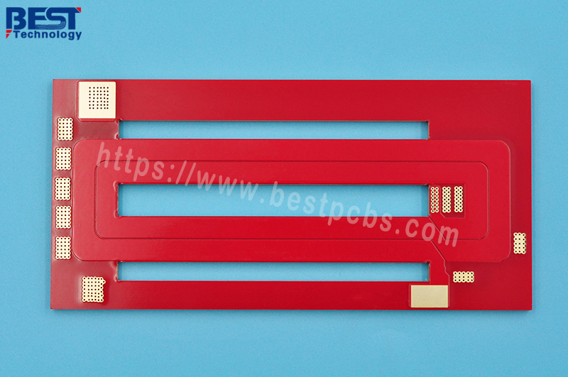
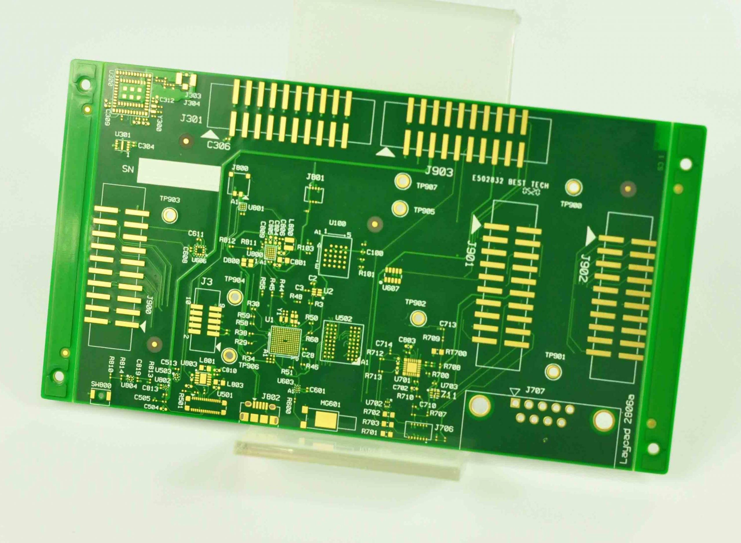
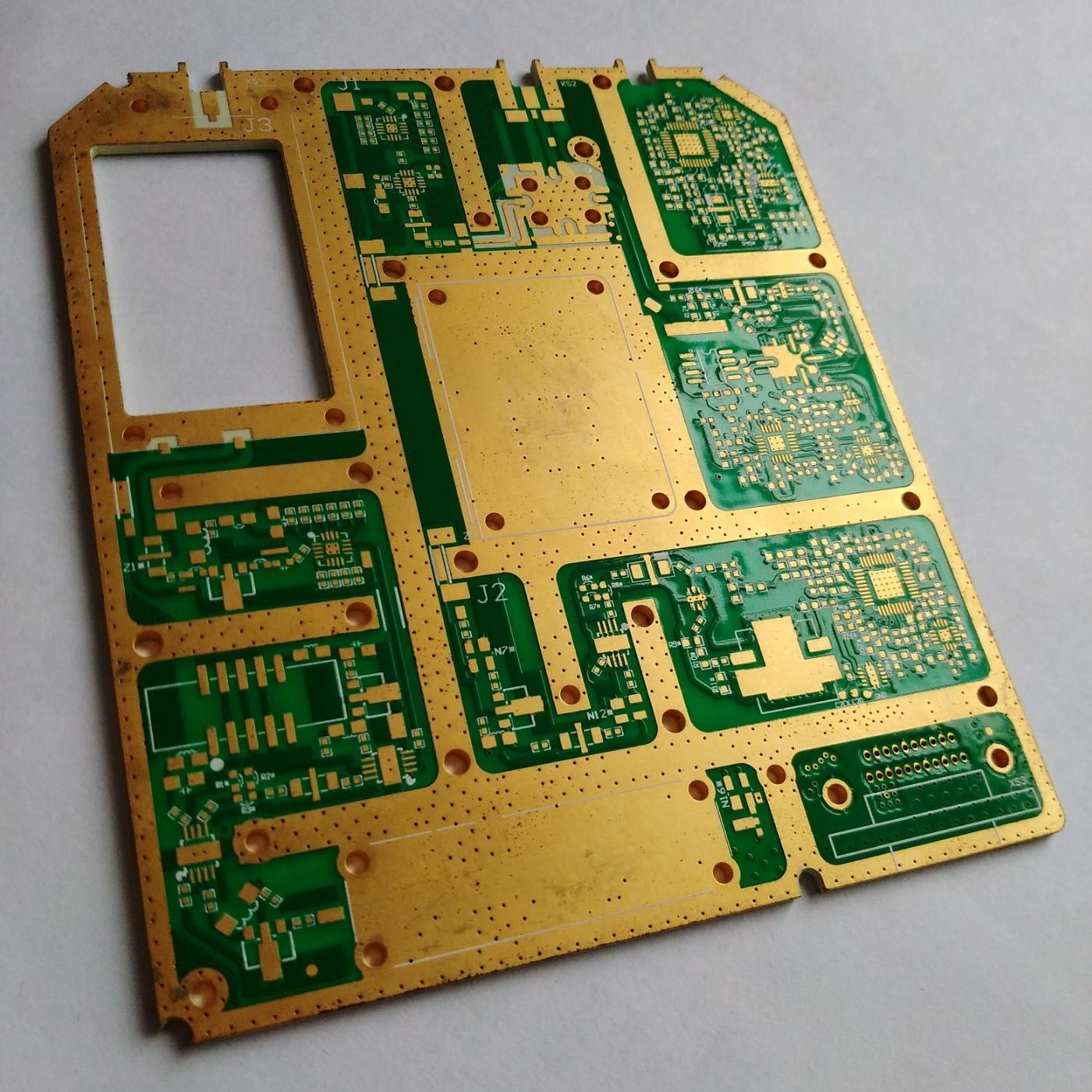
Thick Copper PCB Design, Prototype & Assembly

Thick Copper PCB

Thick Copper PCB Design: Engineers’ Top Pain Points & EBest’s Foolproof Solutions

Common Thick Copper PCB Design Challenges Engineers Face

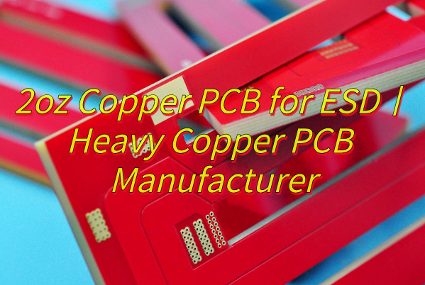
Most engineers struggle with three core issues in thick copper PCB design: improper copper thickness selection, poor heat dissipation, and manufacturability (DFM) issues that lead to rework. Thick copper PCBs (typically ≄3oz copper foil) are designed for high-current, high-heat applications, but incorrect design can cause overheating, soldering failures, or unmanufacturable layouts.

EBest’s Proven Solutions for Thick Copper PCB Design

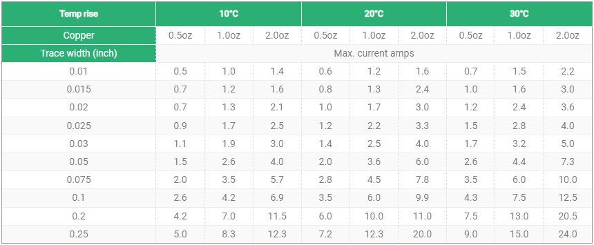
  • Copper Thickness Matching: We help you select the optimal copper thickness (3oz to 20oz) based on your current requirements, using a simple reference formula: Allowed Current (A) ≈ Copper Thickness (oz) × Trace Width (mm) × 0.8 (at ≀40℃). For example, 3oz copper with a 3mm width can handle ~7.2A, making it ideal for most industrial power applications. We avoid over-design (e.g., unnecessary 10oz+ copper) to prevent PCB warping and drilling issues.
  • Heat Dissipation Optimization: For high-power components (e.g., MOSFETs), we add copper pours and thermal vias (0.8-1.2mm diameter, 2-3mm spacing) to transfer heat to inner or ground layers. In medical device PCBs (e.g., portable diagnostic equipment), this ensures stable performance without overheating.
  • DFM Compliance: We optimize trace width and spacing (3oz copper: ≄0.3mm width/spacing; 6oz copper: ≄0.4mm) and use grid copper pouring (2-3mm spacing, 0.2-0.3mm trace width) to avoid etching unevenness and PCB warping. Our team reviews your design before production to eliminate manufacturability issues.

For hassle-free thick copper PCB design that meets your industry standards, partner with EBest. Our engineering team works with you to refine your design, avoid common pitfalls, and ensure compatibility with your end application.

Thick Copper PCB Prototyping: Why Engineers Struggle & EBest’s Fast, Error-Free Fixes

Key Pain Points in Thick Copper PCB Prototyping

Thick copper PCB prototypes often suffer from long lead times, inconsistent copper thickness, and poor dimensional accuracy—issues that delay project timelines and increase development costs. Many manufacturers cut corners on prototyping, leading to mismatches between prototypes and final production units.

EBest’s Thick Copper PCB Prototyping Solutions

  • Rapid Turnaround: We deliver thick copper PCB prototypes in days, not weeks, without sacrificing quality. Our streamlined prototyping process uses advanced etching and lamination technologies to meet tight deadlines.
  • Consistent Quality: We use high-Tg substrates (Tg≄170℃) and precision lamination to ensure uniform copper thickness and dimensional stability. For aerospace prototypes (e.g., satellite communication boards), this ensures compliance with -55℃ to 200℃ temperature cycle requirements.
  • Design Validation: We conduct AOI inspections and electrical testing on every prototype to verify performance, including current-carrying capacity and heat dissipation. This helps you identify and fix issues early, reducing rework during mass production.

Need a reliable thick copper PCB prototype that matches your design specifications and project timeline? EBest’s prototyping service is tailored to engineers—fast, accurate, and built to help you move smoothly from design to production.

Thick Copper PCB Assembly: Common Pitfalls & EBest’s Expert, Reliable Resolutions

Common Thick Copper PCB Assembly Challenges

Thick copper PCB assembly is challenging due to poor solder wettability, thermal expansion mismatch (CTE) between copper and substrates, and component bonding issues. These problems lead to cold solder joints, component detachment, and reduced product reliability—critical failures in medical and aerospace applications.

EBest’s Expert Thick Copper PCB Assembly Solutions

  • Solderability Improvement: We enlarge pads by 0.2-0.3mm (compared to standard PCBs) and adjust reflow soldering parameters (5-10℃ higher than for thin copper PCBs, with a 10-15 second longer holding time) to ensure full solder coverage. For industrial equipment PCBs (e.g., power inverters), this reduces solder voids to <5%.
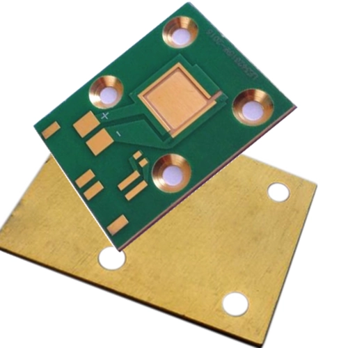
  • CTE Mismatch Resolution: We use copper-clad ceramic substrates (e.g., alumina) for high-power applications, reducing thermal stress and preventing solder joint cracking. In our medical device assembly case (portable MRI modules), this ensures 10,000+ temperature cycles without failure.
  • Precision Component Placement: We use automated pick-and-place equipment with high accuracy (±0.03mm) to handle large components (e.g., TO-220, D2PAK) on thick copper PCBs. Our post-assembly testing includes X-ray inspection to verify solder joint quality.

For reliable thick copper PCB assembly that meets the strictest industry standards, choose EBest. Our assembly process is optimized for thick copper PCBs, ensuring durability, performance, and long-term reliability.

What Makes EBest’s Thick Copper PCB Services Outperform Competitors? (2026 Guide)

Service Aspect

Industry Average

EBest’s Advantage

Copper Thickness Range

3oz-10oz

3oz-20oz, including ultra-thick copper for aerospace applications

Prototype Lead Time

7-10 days

3-5 days, with expedited options available

Industry Expertise

General electronics focus

Specialized in medical, aerospace, and industrial sectors with proven case studies

Quality Testing

Basic electrical testing

AOI, X-ray, temperature cycle, and vibration testing (meets ISO 13485 for medical)

Customization

Limited design adjustments

Full custom solutions, including DFM optimization and material selection

EBest’s Industry Case Studies (Proven Expertise)

  • Medical Industry: We designed and assembled thick copper PCBs for a portable patient monitor, using 3oz copper and high-Tg FR-4 to ensure stable performance in clinical environments. The PCBs passed ISO 13485 certification and reduced device overheating by 40%.
  • Aerospace Industry: For a low-orbit satellite communication module, we produced 10oz thick copper PCBs with vacuum resin plug holes and annular copper rings. The PCBs withstood 10,000 temperature cycles (-55℃⇆125℃) with <2% hole resistance change.
  • Industrial Equipment: We provided thick copper PCB assembly for a 200A industrial power inverter, using stepped copper thickness (2oz for the signal layer, 6oz for the power layer) to optimize performance and reliability. The inverter achieved 99.8% operational uptime.

Thick Copper PCB vs. Standard PCB: Critical Differences Every Engineer Must Know

The key difference between a thick copper PCB and a standard PCB lies in copper foil thickness: thick copper PCBs have a copper thickness of ≄3oz (≈105ÎŒm), while standard PCBs typically use 1oz-2oz copper. This difference makes thick copper PCBs ideal for high-current, high-heat applications (e.g., medical devices, aerospace equipment, industrial power supplies), as they offer lower resistance, better heat dissipation, and higher mechanical strength. Standard PCBs are suitable for low-power electronics (e.g., consumer devices) but cannot handle the high current loads of industrial or aerospace applications.

How to Choose the Right Copper Thickness for Your Thick Copper PCB (Engineer’s Step-by-Step Guide)

Selecting the right copper thickness for your thick copper PCB depends on three factors: current load, application environment, and manufacturability. Follow this simple guide:

  • 3oz-6oz: Ideal for most industrial power supplies, medical devices, and automotive electronics (handles 3A-10A current).
  • 7oz-10oz: Suitable for high-power applications (e.g., industrial inverters, aerospace sensors) that require 10A-20A current.
  • 11oz-20oz: Reserved for ultra-high-power applications (e.g., laser weapons, satellite power systems) that require 20A+ current.

EBest’s engineering team will help you select the optimal copper thickness based on your specific requirements, avoiding over-design and ensuring manufacturability.

Best Materials for Thick Copper PCB Manufacturing: Engineer’s Definitive Guide

The best materials for thick copper PCB manufacturing depend on your application, but we prioritize high-performance, reliable options that meet industry standards:

  • Substrates: High-Tg FR-4 (Tg≄170℃) for most applications; PI (polyimide) for high-temperature environments (e.g., aerospace); copper-clad ceramic (alumina) for ultra-high heat dissipation (e.g., medical lasers).
  • Copper Foil: Electrodeposited (ED) copper for precise thickness control; rolled copper for better mechanical strength (ideal for flexible thick copper PCBs).
  • Solder Mask: Lead-free, high-temperature solder mask (e.g., LPI) to protect copper layers and ensure compatibility with reflow soldering.

How to Guarantee Thick Copper PCB Reliability in Extreme Industrial & Aerospace Environments

To ensure thick copper PCB reliability in extreme environments (high temperature, vibration, humidity), EBest implements three key measures:

  • Material Selection: We use high-Tg substrates and corrosion-resistant copper foil to withstand temperature extremes (-55℃ to 200℃) and humidity (up to 95%).
  • Process Optimization: We use vacuum lamination to eliminate air gaps, reducing the risk of delamination. For vibration-prone applications (e.g., aerospace), we add reinforcing copper rings around vias.
  • Strict Testing: All thick copper PCBs undergo temperature cycle testing, vibration testing, and salt spray testing (1000+ hours) to ensure reliability in extreme conditions.

FAQ: Thick Copper PCB Questions Engineers Actually Ask (Answered by EBest Experts)

1. What is a thick copper PCB, and when should I use it?

A thick copper PCB is a printed circuit board with copper foil thickness ≄3oz (≈105ÎŒm). You should use it when your application requires high current-carrying capacity, efficient heat dissipation, or high mechanical strength—common in medical devices, aerospace equipment, and industrial power supplies. It is not necessary for low-power consumer electronics.

2. Can thick copper PCBs be used in medical devices?

Yes, thick copper PCBs are ideal for medical devices (e.g., portable diagnostic equipment, MRI modules, patient monitors). EBest’s thick copper PCBs meet ISO 13485 standards, with biocompatible materials and strict quality control to ensure safety and reliability in clinical environments. Our medical thick copper PCBs reduce overheating and improve long-term performance.

3. How long does it take to produce a thick copper PCB prototype?

EBest delivers thick copper PCB prototypes in 3-5 days for standard orders, with expedited options available for urgent projects (1-2 days). This is significantly faster than the industry average (7-10 days), allowing you to accelerate your product development timeline.

4. What is the maximum copper thickness EBest can produce?

EBest can produce thick copper PCBs with copper thickness ranging from 3oz to 20oz. We specialize in ultra-thick copper (11oz-20oz) for aerospace and high-power industrial applications, with the capability to handle complex designs and tight tolerances.

5. How does EBest ensure the quality of thick copper PCB assembly?

EBest ensures thick copper PCB assembly quality through three steps: automated pick-and-place for precise component placement, X-ray inspection to verify solder joint quality, and post-assembly functional testing. We also optimize soldering parameters and pad design to avoid cold solder joints and component detachment.

6. Can EBest provide custom thick copper PCB solutions?

Yes, EBest specializes in custom thick copper PCB solutions. Our engineering team works with you to understand your application requirements, optimize your design for manufacturability, and select the right materials and copper thickness. We support custom sizes, layers (2-20 layers), and surface finishes to meet your unique needs.

Choose EBest for Thick Copper PCB: Fast Delivery, Custom Solutions, Proven Industrial/Aerospace Quality

EBest is your trusted partner for thick copper PCB design, thick copper PCB prototype, and thick copper PCB assembly. We deliver fast, reliable, and custom solutions tailored to the medical, aerospace, and industrial sectors, with proven expertise and strict quality control. Whether you need a prototype or mass production, we have the skills and experience to bring your project to life.

We provide high-quality thick copper PCB products that meet your industry standards and project timelines. For inquiries or to place an order, please contact us at sales@bestpcbs.com. EBest—Your Reliable Thick Copper PCB Manufacturer.

Copper Base PCB Design, Prototype & Assembly | Fast Custom Solutions & 24H Expedite Shipping
Thursday, February 26th, 2026

Choose EBest As Your First Copper Base PCB Manufacturer

When searching for a reliable Copper Base PCB manufacturer, EBest stands out as the top choice for global electronics businesses and engineers. Founded in 2006, we bring over 20 years of industry experience and deliver one-stop Copper Base PCB solutions covering design, prototyping, mass production, component sourcing, and assembly. Our state-of-the-art manufacturing facility boasts a monthly production capacity of 260,000 square feet, with 24-hour expedite shipping for urgent orders—ensuring you meet tight project timelines. Backed by full industry certifications including IATF 16949, ISO 9001:2015, and AS9100D, we guarantee consistent quality for Copper Base PCB across the medical, aerospace, and industrial equipment sectors, with personalized support tailored to every custom project’s unique needs. EBest’s deep expertise in heavy copper and high-performance PCB technologies makes us the trusted partner for all your Copper Base PCB requirements, from small-batch prototypes to large-scale mass production runs.

What Do Engineers Care About In Copper Base PCB Design? Solve Pain Points With EBest

Key Design Challenges Engineers Face For Copper Base PCB

Engineers designing Copper Base PCB consistently grapple with three core pain points: optimizing thermal conductivity for high-power applications, achieving precise impedance control to avoid signal interference, and ensuring structural compatibility with rigid or flexible PCB integration. Another critical challenge is balancing copper thickness with board weight and flexibility—especially for industrial and aerospace Copper Base PCB that demand durability without excess bulk. Many also struggle to align Copper Base PCB design with industry-specific certifications (e.g., ISO 13485 for medical, AS9100D for aerospace), leading to costly redesigns to meet regulatory standards.

EBest’s Copper Base PCB Design Solutions For Every Challenge

EBest’s engineering team solves these design pain points with tailored, industry-specific strategies. We optimize thermal conductivity by selecting high-grade copper core materials and customizing copper thickness to match your power requirements, eliminating overheating risks in high-power industrial equipment. Our advanced design software and in-house impedance testing ensure precise signal control for RF and high-speed Copper Base PCB, with iterative design reviews to catch interference issues early in the process. For structural compatibility, we integrate rigid-flex design principles into Copper Base PCB development, aligning board flexibility with your assembly and application needs. Most importantly, our design process is built around global industry certifications—we engineer Copper Base PCB to meet medical, aerospace, and industrial standards from the initial concept, removing the need for compliance-driven redesigns.

Partner With EBest For Your Copper Base PCB Design Needs

Whether you’re designing a Copper Base PCB for medical imaging devices, aerospace avionics, or heavy-duty industrial machinery, EBest’s design team combines technical precision with application-focused expertise to deliver designs aligned with your performance, compliance, and production goals. Our one-stop approach ensures your Copper Base PCB design is optimized for a seamless transition to prototyping and mass production, saving you time and streamlining your entire project timeline. Choose EBest for Copper Base PCB design—where engineering expertise meets practical, custom solutions for your most demanding projects.

Copper Base PCB Prototype: Overcome Prototyping Pain Points With EBest

Top Prototyping Pain Points For Copper Base PCB

Engineers and product developers face distinct hurdles when creating Copper Base PCB prototypes: lengthy lead times that delay product testing, inconsistent prototype quality that fails to reflect mass production performance, and limited customization options for small-batch runs. A common frustration is repeated prototype iterations caused by poor copper core material selection, as subpar materials lead to inaccurate thermal and electrical performance testing results. Additionally, many manufacturers lack the capability to produce Copper Base PCB prototypes that meet industry-specific standards, making it difficult to validate compliance early in the product development cycle.

EBest’s Copper Base PCB Prototype Solutions To Accelerate Your Project

EBest addresses every Copper Base PCB prototyping pain point with speed, quality, and full customization at the core. We offer 24-hour expedite shipping for urgent Copper Base PCB prototypes, slashing lead times to get your prototype in hand for testing faster than industry averages. Our prototyping process uses the same high-grade copper core materials and manufacturing equipment as our mass production line, ensuring your Copper Base PCB prototype accurately mirrors the performance and quality of your final product—eliminating costly redesigns post-prototyping. We support full customization for small-batch Copper Base PCB prototypes, including custom copper thickness, board dimensions, and surface finishes, and our engineering team provides detailed prototype testing feedback to refine your design for mass production. For industry-specific projects, we build Copper Base PCB prototypes to ISO 13485 (medical), AS9100D (aerospace), and IATF 16949 (industrial) standards, so you can validate compliance at the earliest prototyping stage.

Choose EBest For Your Copper Base PCB Prototype Development

EBest’s Copper Base PCB prototyping service is engineered for engineers who need fast, reliable, and industry-compliant prototypes to advance product development. Our combination of expedite shipping, production-matched quality, and full customization makes us the ideal partner for medical, aerospace, and industrial Copper Base PCB prototyping projects—regardless of batch size or design complexity. Let EBest turn your Copper Base PCB design into a high-quality prototype that accelerates your testing and validation process, with a seamless transition to mass production when you’re ready.

Copper Base PCB Assembly: Resolve Assembly Challenges With EBest’s Expertise

Critical Assembly Pain Points For Copper Base PCB

Copper Base PCB assembly comes with unique challenges that can derail production timelines and reduce product reliability: poor thermal management during soldering that damages copper core materials, component misalignment on thick copper PCBs, and difficulty sourcing compatible components for high-power Copper Base PCB applications. Engineers also struggle with assembly processes that fail to meet the strict quality standards of the medical and aerospace industries, leading to high defect rates and costly rework. Another common issue is limited assembly flexibility for custom Copper Base PCB designs, as many manufacturers use one-size-fits-all assembly processes that do not account for the unique properties of copper core PCBs.

EBest’s Copper Base PCB Assembly Solutions For Flawless Production

EBest’s Copper Base PCB assembly service leverages specialized equipment and industry expertise to solve these challenges for medical, aerospace, and industrial projects. We use temperature-controlled soldering processes for Copper Base PCB assembly, preventing thermal damage to copper core materials and ensuring strong, reliable solder joints—critical for high-power applications. Our automated assembly line features high-precision component placement technology, eliminating misalignment issues even on thick, heavy copper Copper Base PCB. As a one-stop provider, we offer full component sourcing for Copper Base PCB assembly, matching high-quality, industry-compliant components to your design’s power and performance requirements—saving you time and guaranteeing component compatibility. Our assembly process is certified to ISO 13485, AS9100D, and IATF 16949, so your Copper Base PCB assembly meets the strict quality and compliance standards of the medical, aerospace, and industrial equipment industries, with zero-defect production as our core goal. We also provide flexible assembly processes for custom Copper Base PCB designs, tailoring our approach to your board’s unique properties and assembly requirements.

Trust EBest For Your Copper Base PCB Assembly Needs

Whether you need small-batch or large-scale Copper Base PCB assembly for medical devices, aerospace systems, or industrial machinery, EBest’s one-stop assembly service delivers uncompromising quality, full compliance, and on-time delivery. Our integration of component sourcing, precision assembly, and industry certification ensures your Copper Base PCB assembly process is seamless from start to finish, with no gaps in quality or regulatory compliance. Choose EBest for Copper Base PCB assembly—where specialized copper core expertise meets reliable, scalable production for all your PCB projects.

Why Choose EBest For Your Copper Base PCB Projects?

EBest is the premier choice for Copper Base PCB design, prototyping, and assembly for three core reasons: 20+ years of specialized copper core expertise, end-to-end one-stop solutions, and industry-leading quality and compliance. Our team of PCB engineers has deep experience in Copper Base PCB technologies for the medical, aerospace, and industrial equipment sectors, with a proven track record of delivering custom solutions that meet the most demanding performance requirements. As a one-stop provider, we handle every step of your Copper Base PCB project—from initial design and prototyping to mass production, component sourcing, and assembly—eliminating the need to work with multiple vendors and streamlining your project timeline. Our manufacturing facility is certified to IATF 16949, ISO 9001:2015, ISO 13485:2016, AS9100D, REACH, RoHS, and UL, so every Copper Base PCB we produce meets global industry standards for quality, safety, and compliance. We also offer unrivaled speed, with 24-hour expedite shipping for urgent Copper Base PCB orders and a monthly production capacity of 260,000 square feet (28,900 square meters) to support both small-batch prototypes and large-scale mass production. EBest prioritizes customer satisfaction, with personalized support for every Copper Base PCB project—our team works closely with you to understand your unique needs and deliver tailored solutions aligned with your product goals. Finally, our ongoing commitment to research and development ensures we stay ahead of industry trends in Copper Base PCB technology, continuously innovating our design, prototyping, and assembly processes to deliver the most advanced copper core PCB solutions for your business.

Copper Base PCB Vs Aluminum Base PCB: A Comparative Analysis

FeatureCopper Base PCBAluminum Base PCB
Thermal ConductivityExceptionally high—ideal for high-power applications (100W+); copper core dissipates heat faster and more evenlyModerate thermal conductivity; suitable for low-to-medium power applications (under 100W)
Electrical ConductivitySuperior electrical conductivity; minimal signal loss for high-speed and RF Copper Base PCBLower electrical conductivity; higher signal loss for high-speed applications
Durability & StrengthHigher mechanical strength; resistant to vibration and shock—perfect for aerospace and industrial equipmentLightweight but lower mechanical strength; less suitable for heavy-duty industrial or aerospace use
Copper Thickness FlexibilityCustomizable heavy copper thickness (including ultra-thick copper); tailored to exact power requirementsLimited metal thickness options; not ideal for heavy copper applications
Application SuitabilityMedical imaging devices, aerospace avionics, high-power industrial machinery, RF equipmentConsumer electronics, low-power industrial devices, LED lighting, small-scale power electronics
Compliance CompatibilityEasy to manufacture to ISO 13485 (medical), AS9100D (aerospace), IATF 16949 (industrial)Compliant for consumer and low-power industrial standards; less commonly used for medical/aerospace applications

Copper Base PCB Applications In Medical, Aerospace & Industrial Sectors

Copper Base PCB For Medical Equipment

Copper Base PCB is a critical component in high-power medical equipment, where thermal management and regulatory compliance are non-negotiable. EBest’s medical Copper Base PCB is integrated into medical imaging devices (CT scanners, MRI machines) and high-power diagnostic equipment, where the high thermal conductivity of copper core materials prevents overheating and ensures consistent, reliable performance. All our medical Copper Base PCB is manufactured to ISO 13485:2016 standards, meeting the strict quality and safety requirements of the medical industry, with precise impedance control to avoid signal interference in sensitive diagnostic equipment.

Copper Base PCB For Aerospace Systems

Aerospace avionics and flight systems demand Copper Base PCB that delivers high thermal conductivity, superior mechanical strength, and full compliance with AS9100D standards. EBest’s aerospace Copper Base PCB is used in satellite communication systems, aircraft avionics, and aerospace power modules—our custom copper thickness and rigid-flex design integration ensure the PCB can withstand the extreme vibration, shock, and temperature conditions of aerospace environments. The superior electrical conductivity of our Copper Base PCB also minimizes signal loss for high-speed RF and communication systems in aerospace applications.

Copper Base PCB For Industrial Equipment

Heavy-duty industrial machinery (factory automation, power distribution, heavy manufacturing) relies on Copper Base PCB for high-power performance and long-term durability. EBest’s industrial Copper Base PCB is designed for IATF 16949 compliance, with heavy copper thickness and temperature-resistant materials to handle the high-power and harsh operating conditions of industrial equipment. Our Copper Base PCB for industrial use also features precise component placement and soldering, ensuring zero defects and reliable performance in 24/7 industrial operations.

How To Optimize Thermal Conductivity For Copper Base PCB?

Optimizing thermal conductivity is the most critical step in Copper Base PCB design for high-power applications, and the solution lies in strategic material selection, copper core design, and board layout—with EBest’s engineering team following a proven, step-by-step process for maximum thermal performance. First, select a high-purity copper core material for your Copper Base PCB; high-purity copper has superior thermal conductivity compared to low-grade copper, ensuring faster and more efficient heat dissipation. Second, customize the copper thickness to match your exact power requirements—thicker copper cores dissipate more heat for high-power applications, and EBest offers flexible copper thickness options for every Copper Base PCB design. Third, design the Copper Base PCB layout with thermal vias placed strategically to transfer heat from the copper core to the board’s surface and heat sinks, eliminating hotspots that cause performance issues and component failure. Fourth, use thermal interface materials (TIMs) in conjunction with your Copper Base PCB to enhance heat transfer to external cooling systems, such as heat sinks or fans. EBest’s engineering team tests every Copper Base PCB design for thermal conductivity, using advanced thermal imaging technology to identify and eliminate hotspots before prototyping—ensuring your Copper Base PCB delivers optimal thermal performance for your specific application.

What Industry Certifications Do Copper Base PCB Require?

Copper Base PCB certifications vary by industry, and compliance is non-negotiable for medical, aerospace, and industrial applications—EBest manufactures all Copper Base PCB to the specific certifications required for your project, eliminating compliance risks and costly redesigns. For medical copper base PCB, the core certification is ISO 13485:2016, which sets strict quality management standards for medical devices and their components, ensuring uncompromising safety, reliability, and full traceability. For aerospace Copper Base PCB, AS9100D is the mandatory certification, covering the unique quality and performance requirements of aerospace systems, including resistance to extreme environmental conditions. For industrial Copper Base PCB, IATF 16949 and ISO 9001:2015 are the key certifications, setting global quality standards for automotive and general industrial equipment manufacturing. All EBest Copper Base PCB also complies with REACH, RoHS, and UL standards, ensuring environmental safety and electrical safety for global markets. Our manufacturing process is built around these certifications, with strict quality control checks at every stage of Copper Base PCB design, prototyping, and assembly to maintain full compliance at all times.

FAQ: Common Questions About Copper Base PCB Answered

Q1: What is the maximum copper thickness EBest offers for Copper Base PCB?

EBest offers fully customizable copper thickness for Copper Base PCB, from standard thin copper to ultra-heavy copper options—all tailored to the power and thermal requirements of your medical, aerospace, or industrial application. Our engineering team will recommend the optimal copper thickness for your Copper Base PCB design, balancing thermal conductivity, mechanical strength, and board flexibility for your specific use case.

Q2: Can EBest produce rigid-flex Copper Base PCB for custom applications?

Yes, EBest’s engineering team specializes in integrating rigid-flex design principles into Copper Base PCB manufacturing, producing custom rigid-flex copper core PCBs for aerospace and industrial applications that demand both flexibility and high thermal conductivity. Our rigid-flex Copper Base PCB is designed to meet the same industry certifications and performance standards as our standard copper core PCBs.

Q3: What lead times does EBest offer for Copper Base PCB mass production?

EBest’s standard lead times for Copper Base PCB mass production align with industry best practices, and we offer 24-hour expedite shipping for urgent orders—critical for time-sensitive medical, aerospace, and industrial projects. Our monthly production capacity of 260,000 square feet ensures we can scale production seamlessly to meet your large-batch Copper Base PCB needs with no delays.

Q4: Does EBest provide component sourcing for Copper Base PCB assembly?

Yes, as a one-stop Copper Base PCB provider, EBest offers full component sourcing for assembly, matching high-quality, industry-compliant components to your Copper Base PCB design’s power, performance, and compliance requirements. We source components from trusted global suppliers, ensuring perfect compatibility and long-term reliability for your medical, aerospace, or industrial project.

Q5: How does EBest test Copper Base PCB for thermal and electrical performance?

EBest uses advanced in-house testing technology to validate every Copper Base PCB’s thermal and electrical performance: thermal imaging for heat dissipation and hotspot detection, precision impedance testing for high-speed and RF copper core PCBs, and comprehensive electrical performance testing to ensure minimal signal loss and maximum power efficiency. All testing is completed before prototyping and mass production, to ensure your Copper Base PCB meets or exceeds your performance goals.

Q6: Is EBest’s Copper Base PCB compliant with global environmental standards?

Yes, all EBest Copper Base PCB is fully compliant with REACH and RoHS environmental standards, eliminating hazardous substances and ensuring your product can be sold in global markets without environmental compliance issues. Our manufacturing process also prioritizes sustainability, with waste reduction and eco-friendly production practices for all Copper Base PCB projects.

Q7: Can EBest create custom Copper Base PCB for low-volume, high-complexity projects?

Absolutely—EBest supports full customization for low-volume, high-complexity Copper Base PCB projects, including medical and aerospace applications that demand unique design and performance requirements. Our small-batch prototyping and production capabilities mean we can deliver high-quality, custom Copper Base PCB for low-volume projects with the same speed and compliance as large-scale production.

Q8: What post-production support does EBest offer for Copper Base PCB projects?

EBest provides comprehensive post-production support for all Copper Base PCB projects, including detailed performance testing feedback, expert assembly guidance, and ongoing technical support for your product development and production processes. Our team is available to answer any technical questions and provide tailored solutions for any Copper Base PCB performance or assembly issues you may encounter.

Order Your Custom Copper Base PCB From EBest Today

EBest is your trusted partner for Copper Base PCB design, prototyping, assembly, and mass production—offering one-stop custom solutions for the medical, aerospace, and industrial equipment industries. Our 20+ years of copper core expertise, industry-leading certifications, 24-hour expedite shipping, and personalized engineering support ensure your Copper Base PCB project is a success, from initial concept to final production. We manufacture all types of Copper Base PCB, including heavy copper, high TG, impedance control, and rigid-flex copper core PCBs, with full customization to match your unique performance, compliance, and production needs. Whether you need a small-batch prototype or large-scale mass production, EBest has the capacity, expertise, and uncompromising quality to deliver your Copper Base PCB on time and to the highest global industry standards. To order your custom Copper Base PCB or discuss your project requirements in detail, send an email to sales@bestpcbs.com—our team of dedicated PCB engineers will respond promptly and work with you to create the perfect copper core PCB solution for your business.

Premium Heavy Copper PCB Manufacturer: Meet IPC-A-610 Standard for Your Projects
Thursday, January 22nd, 2026

In power-dense electronics, standard PCB construction often becomes the limiting factor rather than the circuit design itself. Excessive temperature rise, copper fatigue, and current bottlenecks are common failure modes once current levels move beyond conventional ranges. This is where a reliable heavy copper PCB manufacturer stands out. Heavy copper PCBs are engineered specifically to handle high current, elevated thermal loads, and demanding mechanical stress while maintaining long-term reliability.

At Best Technology, we specialize in manufacturing premium heavy copper PCBs that meet and exceed IPC-A-610 requirements, tailored to the unique needs of high-power electronics. In this blog, we’ll break down everything you need to know about heavy copper PCBs—from what defines them to how to choose the right manufacturer, plus real-world case studies and answers to your most pressing questions.

What Makes a PCB “Heavy Copper”?

A PCB is typically classified as heavy copper when the finished copper thickness on one or more layers exceeds 3 oz/ftÂČ (≈105 ”m). Many industrial designs extend well beyond this threshold, reaching 6 oz, 10 oz, or even 20 oz copper, depending on current and thermal requirements.

Unlike standard boards, heavy copper PCBs are not simply “thicker copper versions” of conventional designs. They require dedicated imaging, etching, plating, and lamination strategies to maintain conductor geometry, dielectric integrity, and layer-to-layer registration.

What Makes a PCB “Heavy Copper”?

Why Heavy Copper Matters in High-Power Electronics?

As power electronics continue to shrink in size, current density inevitably increases. Heavy copper construction directly addresses this challenge by offering:

  • Higher current-carrying capacity without excessive temperature rise
  • Lower conductor resistance, improving energy efficiency
  • Improved thermal spreading, reducing hot spots
  • Enhanced mechanical strength, especially around plated through holes and power vias

In applications such as EV power modules, industrial motor drives, and renewable energy converters, heavy copper is often the difference between theoretical performance and field reliability.

Technical Specifications: Copper Weight & Conductivity

Copper thickness is usually specified in ounces per square foot, but its real impact is seen in electrical and thermal performance.

Typical heavy copper parameters include:

  • Copper thickness: 3 oz to 20+ oz (105 ”m to >700 ”m)
  • Trace current capacity: Several times higher than 1-oz copper at equivalent temperature rise
  • Lower voltage drop: Especially critical for low-voltage, high-current systems
  • Thermal conductivity: Copper’s intrinsic conductivity enables efficient heat spreading across planes and embedded power structures

A qualified heavy copper PCB manufacturer will validate these parameters against IPC guidelines rather than relying on theoretical calculations alone.

Heavy Copper PCB Manufacturing Challenges

Manufacturing heavy copper PCBs is more complex than standard ones, requiring specialized equipment and strict quality control. Key challenges we address at Best Technology:

  • Etching Uniformity: Thicker copper is hard to etch evenly, causing uneven traces or undercutting. We use controlled depth etching and precision equipment for consistent, clean traces.
  • Plating Consistency: Multilayer PCBs need thick, uniform via plating. Our optimized electroplating ensures reliable via connections, avoiding high resistance or thermal failure.
  • Thermal Stress: Copper and substrates (e.g., FR-4) expand differently under heat, causing warping or delamination. We use temperature-controlled lamination to minimize stress.
  • IPC-A-610 Compliance: Meeting this standard (trace geometry, plating, solder joints) requires rigorous quality control at every manufacturing stage.
Heavy Copper PCB Manufacturing Challenges

Design Guidelines for Heavy Copper PCB

Heavy copper PCB design should follow one core principle: current-driven, precisely matched copper. Simply increasing copper thickness often raises cost and introduces new risks, including uneven heat dissipation, soldering difficulty, and mechanical stress. Effective heavy copper design balances electrical demand with manufacturability.

1. Copper Thickness Selection

Choose copper thickness based on actual current, not excessive margin.

Formula (ambient ≀ 40 °C):

Allowable current (A) ≈ Copper thickness (oz) × Trace width (mm) × 0.8

For example:

3 oz copper × 3 mm trace ≈ 7.2 A, suitable for most industrial power designs.

Recommendations:

  • Prefer 3–6 oz, which covers most applications
  • Above 10 oz increases risks of warpage and drilling difficulty
  • Avoid overdesign unless required by aerospace or defense systems

2. Trace Design for High Current

Trace geometry must support smooth current flow.

  • 3 oz copper: minimum trace width ≄ 0.3 mm
  • 6 oz copper at 10 A: recommended width ≄ 5 mm

Avoid sudden width changes. Use gradual tapers (length ≄ 3× width difference) to prevent current crowding and localized heating.

For thermal control, use copper pours under power devices combined with thermal vias (Ø 0.8–1.2 mm, pitch 2–3 mm) to transfer heat into internal planes.

3. Via Design Considerations

Vias are a critical limitation point in heavy copper PCBs.

  • Minimum finished hole ≄ 0.8 mm (3 oz copper)
  • Via wall copper ≄ 20 ”m

Do not rely on a single via for high current. A 5 A path on 3 oz copper typically requires 2–3 parallel vias, as one via carries only 2–3 A reliably.

Ensure adequate solder mask opening (hole + 0.2–0.3 mm) to prevent solder blockage.

4. Stack-Up and Material Selection

Place heavy copper layers on outer or near-outer layers and keep copper distribution symmetrical to prevent warpage.

Select high-Tg materials (Tg ≄ 170 °C), such as FR-4 Tg170 or polyimide, to withstand higher thermal load during assembly and operation.

5. Assembly Adaptation

Heavy copper absorbs more heat during soldering.

  • Use large power packages (e.g., TO-220, D2PAK)
  • Enlarge pads by 0.2–0.3 mm compared to standard designs
  • Increase reflow peak temperature by 5–10 °C and extend soak time by 10–15 s to avoid cold solder joints

Top Industries Using Heavy Copper PCBs

Heavy copper PCBs are widely used in industries that demand power, durability, and reliability:

  • Power supplies & converters
  • Electric vehicles (EV) & charging systems
  • Industrial motor drives
  • Renewable energy (solar, wind, inverters)
  • Aerospace & defense electronics
  • Medical imaging and power modules

These industries rely on certified heavy copper PCB manufacturers to meet strict quality standards.

How to Choose a Heavy Copper PCB Manufacturer?

Choosing the right heavy copper PCB manufacturer is a strategic decision that directly affects product quality and lifecycle cost.

Important evaluation criteria include:

  • Proven experience with multi-ounce copper designs
  • Clear alignment with IPC-A-610 and IPC-6012 standards
  • Robust process control and inspection capability
  • Engineering support for DFM and design optimization
  • Ability to scale from prototype to volume production

Manufacturers that lack dedicated heavy copper expertise often struggle with yield, consistency, and long-term reliability.

Why Choose Best Technology as Your Heavy Copper PCB Manufacturer?

With over 20 years of experience in heavy copper PCB manufacturing, Best Technology has the expertise to handle even the most complex projects—from standard heavy copper (3 oz – 5 oz) to extra-thick copper (up to 20 oz). Our team of engineers specializes in solving the unique challenges of heavy copper PCB design and manufacturing.

We offer fully customized heavy copper PCBs to meet your project’s unique requirements. Whether you need a specific copper weight, substrate, surface finish, or board size, we can tailor our solutions to fit your needs.

We deeply know the importance of quality for every product, so we ensure the full traceability from design, manufacturing to shipment. We strictly adhere to IPC-A-610 standards (Class 2 and Class 3) for every heavy copper PCB we manufacture. In addition to this, due to heavy copper PCB always used in electric vehicles, our facility obtained the IATF16949 and AS9100D certifications to ensure each process are under rigorous control.

Heavy Copper PCB Case Studies in Best Technology

Case Study 1: EV Battery Management System (BMS) PCB

Customer: A leading global automotive manufacturer specializing in electric vehicles.

Challenge: The customer needed a heavy copper PCB for their EV BMS that could handle high currents (up to 200A), dissipate heat efficiently, and meet IPC-A-610 Class 3 standards. The PCB also needed to be compact to fit within the EV’s battery pack.

Solution: We designed and manufactured a 6 oz heavy copper PCB using high-temperature FR-4 substrate and ENIG surface finish. We integrated copper pours and thermal vias to improve thermal management, and optimized the trace width and spacing to handle the high current load. We also used blind vias to save space, ensuring the PCB fit within the customer’s compact design.

Result: The PCB met all IPC-A-610 Class 3 requirements, handled the 200A current load without overheating, and reduced the BMS’s overall size by 15%. The customer has since expanded their partnership with us for all their EV BMS PCB needs.

Heavy Copper PCB Case Studies in Best Technology

Case Study 2: Solar Inverter PCB

Customer: A renewable energy company specializing in solar inverters.

Challenge: The customer needed a heavy copper PCB for their 50kW solar inverter that could handle high voltages (up to 1000V) and dissipate heat in outdoor environments. The PCB also needed to be durable enough to withstand extreme temperature fluctuations (-40°C to 85°C).

Solution: We manufactured a 10 oz heavy copper PCB using polyimide substrate (for high-temperature resistance) and immersion silver surface finish (for excellent conductivity). We designed the PCB with wide traces (0.030 inches) to handle the high voltage and current, and integrated large copper pours to dissipate heat. We also used a conformal coating to protect the PCB from outdoor elements.

Result: The PCB operated reliably in extreme temperature conditions, handled the 1000V voltage load without failure, and reduced the inverter’s heat-related downtime by 80%. The customer reported a 20% increase in inverter efficiency due to the PCB’s superior thermal management.

Heavy Copper PCB Case Studies in Best Technology

Our Heavy Copper PCB Manufacturing Capabilities

At Best Technology, we have the capabilities to handle all your heavy copper PCB needs—from prototype to production. Here’s a breakdown of our key manufacturing capabilities:

  • Base Material: FR4/Aluminum
  • Copper Weight: 3 oz – 20 oz (105 ÎŒm – 700 ÎŒm) for single-sided, double-sided, and multilayer PCBs.
  • Extreme Heavy Copper: 20-200OZ
  • Outline: Routing, punching, V-cut
  • Layer Count: 1 layer – 40 layers (multilayer heavy copper PCBs with blind/buried vias available).
  • Surface Finishes: HASL, ENIG, OSP, Immersion gold
  • Solder Mask: White, Black, Blue, Green, Red
  • Tolerances: Trace width tolerance ±0.001 inches, copper thickness tolerance ±10%, board thickness tolerance ±0.005 inches.
  • Board Size: Up to 24 inches x 36 inches (609.6 mm x 914.4 mm), with custom sizes available.
  • Quality Control: X-ray inspection, optical inspection (AOI), flying probe testing, thermal cycling testing, and IPC-A-610 compliance testing.
  • Production Capacity: Prototype runs (1 – 100 units), small batch production (100 – 1000 units), and large-scale production (1000+ units) with lead times as short as 3 days for prototypes.
  • Support for prototypes, small batches, and stable mass production

FAQs About Heavy Copper PCBs

1. When should I choose a heavy copper PCB over a standard PCB?

    Choose a heavy copper PCB if your project requires:

    • High current carrying capacity (more than 10A).
    • Enhanced thermal management (e.g., applications operating at high temperatures or generating significant heat).
    • Greater mechanical strength (e.g., rugged industrial or automotive applications).
    • Reduced component count (replacing discrete heat sinks or bus bars).

    Standard PCBs are sufficient for low-power applications (e.g., consumer electronics with low current demands).

    2. How is heavy copper PCB manufacturing different from standard PCB manufacturing?

    Heavy copper PCB manufacturing requires specialized processes to handle the thicker copper layers, including:

    • Controlled depth etching to ensure uniform trace widths and clean edges.
    • Optimized electroplating processes to ensure consistent via plating thickness.
    • Temperature-controlled lamination to minimize thermal stress and prevent warping/delamination.
    • Rigorous quality control to meet IPC-A-610 standards, including X-ray inspection for via integrity.

    Standard PCB manufacturing uses simpler etching and plating processes, as the thinner copper layers are easier to handle.

    3. Are heavy copper PCBs more expensive?

    Yes, heavy copper PCBs are typically more expensive than standard PCBs. The higher cost is due to:

    • More copper material (thicker layers require more copper).
    • Specialized manufacturing processes (e.g., controlled etching, optimized plating).
    • Rigorous quality control (e.g., X-ray inspection, thermal testing).

    However, the extra cost is often offset by the benefits: reduced component count, longer lifespan, improved reliability, and lower maintenance costs. For high-power applications, heavy copper PCBs are a cost-effective long-term investment.

    4. How does copper thickness influence current carrying capacity?

    Copper thickness has a direct impact on current carrying capacity: thicker copper layers have lower electrical resistance, allowing them to carry more current without overheating. As a general rule, the current carrying capacity of a copper trace increases linearly with copper thickness. For example:

    • 1 oz copper trace (35 ÎŒm): ~5A current carrying capacity (at 25°C temperature rise).
    • 3 oz copper trace (105 ÎŒm): ~15A current carrying capacity (at 25°C temperature rise).
    • 10 oz copper trace (350 ÎŒm): ~50A current carrying capacity (at 25°C temperature rise).

    A reputable heavy copper PCB manufacturer will help you select the right copper thickness based on your project’s current requirements and thermal constraints.

    5. Can heavy copper PCBs be multilayered?

    Yes, heavy copper PCBs can be multilayered. Multilayer heavy copper PCBs are used in high-power applications that require both high current carrying capacity and complex circuitry (e.g., EV BMS, solar inverters, aerospace systems). We specialize in manufacturing multilayer heavy copper PCBs with up to 40 layers, including blind and buried vias to save space and improve signal integrity.

    6. How to avoid heat-related failures in heavy copper PCBs?

    To avoid heat-related failures, follow these best practices:

    • Use thick copper layers (3 oz or more) to dissipate heat efficiently.
    • Integrate thermal management features like copper pours, thermal vias, and heat sinks.
    • Choose a high-temperature substrate (e.g., polyimide) for applications operating at extreme temperatures.
    • Optimize trace design (wider traces) to reduce resistance and heat generation.
    • Work with a heavy copper PCB manufacturer that adheres to IPC-A-610 standards, ensuring proper plating and trace integrity.

    Ready to Start Your Heavy Copper PCB Project?

    If you’re working on a high-power electronics project that requires premium heavy copper PCBs—ones that meet IPC-A-610 standards, deliver superior performance, and fit your budget—look no further than Best Technology. As a trusted heavy copper PCB manufacturer with over 20 years of experience, we have the expertise, equipment, and dedication to bring your project to life.

    Here’s how to get started:

    1. Share Your Requirements: Send us your PCB design files, copper weight needs, substrate preferences, and application details.

    2. Get a Custom Quote: Our team will review your requirements and provide a competitive, no-obligation quote within 24 hours.

    3. Design Support (If Needed): Our engineers will work with you to optimize your design for performance, manufacturability, and cost.

    4. Manufacturing & Delivery: We’ll manufacture your heavy copper PCBs to IPC-A-610 standards, conduct rigorous quality control, and deliver them on time—whether you need prototypes or large-scale production.

    Don’t settle for subpar heavy copper PCBs that put your project at risk. Choose Best Technology—the premium heavy copper PCB manufacturer that delivers reliability, performance, and peace of mind. Contact us today to discuss your heavy copper PCB project!

    3 oz Copper PCB Design & ManufactureräžšEBest Circuit (Best Technology)
    Wednesday, August 6th, 2025

    What is 3 oz copper PCB? Let’s explore thickness, current capability, advantages, applications, design guide and how to get a quote for 3 oz copper PCB.

    Are you troubled with these issues?

    • PCB temperature rises uncontrollably under high current conditions. How can I overcome the heat dissipation bottleneck?
    • What should I do if impedance fluctuations increase bit error rates during high-frequency signal transmission?
    • The copper thickness compliance rate for multilayer boards is low after lamination. How can I ensure consistent quality?

    EBest Circuit (Best Technology) can provide solution:

    • Micro-etching + electroplating fill process: Using proprietary surface treatment technology, we achieve a 3oz copper thickness tolerance of ±8ÎŒm, improving heat dissipation efficiency by 40%.
    • Impedance simulation and compensation design: Provide pre-DFM analysis services to proactively compensate for the impact of copper thickness on impedance, ensuring signal loss <3dB
    • Vacuum lamination intelligent temperature control system: Using a segmented pressurization process to eliminate delamination issues in heavy copper clad plates, maintaining a stable yield rate above 98.5%.

    Welcome to contact us if you have any request for 3 oz copper PCB: sales@bestpcbs.com.

    What Is 3 oz Copper PCB?

    A 3 oz copper PCB is a type of ‌heavy copper PCB‌ that features a copper thickness of 3 ounces per square foot, significantly thicker than standard 1 oz (35 ”m) PCBs. This design is ideal for high-power applications, such as power supplies, automotive electronics, and industrial equipment, where it can handle higher current loads, dissipate heat more effectively, and enhance mechanical durability. The increased copper thickness also reduces resistance and improves thermal management, making it a reliable choice for demanding environments.

    What Is 3 oz Copper PCB?

    How Thick is 3 oz of Copper on a PCB?

    3 oz of copper on a PCB measures approximately 105 micrometers (”m) in thickness, equivalent to 4.13 mils, which is three times thicker than standard 1 oz (35”m) copper foil. This thickness is calculated based on the weight of copper per square foot, where 1 oz equals 28.35 grams spread over 1 square foot (0.0929 mÂČ), with 3 oz representing three times that mass density.

    How Thick is 3 oz of Copper on a PCB?

    What Is the Current of 3 oz Copper PCB?

    A 3 oz (105”m) copper PCB can typically handle 22–30A per 1mm width at a 20°C temperature rise, depending on whether the trace is on the inner or outer layer (inner layer: ~22A/mm; outer layer: ~30A/mm). This capacity is derived from IPC-2221 standards, which consider copper thickness, trace width, and allowable temperature rise. For example, a 10mm-wide trace on an outer layer could theoretically carry 300A with proper thermal management.

    Why Choose 3 oz Copper PCB?

    • Higher Current Capacity – Supports up to 30A/mm on outer layers, enabling stable operation for high-power applications without excessive heating.
    • Improved Thermal Management – Thicker copper dissipates heat more efficiently, reducing thermal stress and prolonging component lifespan.
    • Enhanced Durability – Resists mechanical stress and thermal cycling better than thinner copper, ideal for demanding environments.
    • Space Efficiency – Allows for wider traces or fewer layers in high-current designs, simplifying PCB layouts and reducing costs.
    • Reliable Performance – Minimizes voltage drop and signal loss, ensuring consistent power delivery in industrial and automotive applications.

    When to Use 3oz Copper PCB?

    • High-Current Power Applications: Power supplies, motor controllers, battery management systems (BMS), and solar inverters require thick copper (3oz) to minimize resistive losses and heat generation under heavy loads.
    • Thermal Management-Critical Systems: Automotive engine control units (ECUs), industrial power converters, and LED drivers use 3oz copper to enhance heat dissipation, reducing reliance on external heatsinks.
    • RF/Microwave Power Amplifiers: Thick copper layers improve current handling in high-frequency power circuits, minimizing signal loss and thermal stress in wireless communication/radar systems.
    • Mechanically Demanding Environments: Aerospace, military, and automotive PCBs subject to vibration, shock, or thermal cycling use 3oz copper for structural durability and reduced risk of trace fatigue.
    • Corrosion-Resistant/Outdoor Electronics: Marine, industrial automation, and outdoor IoT devices benefit from thicker copper’s resistance to humidity, salt, and chemical exposure, ensuring long-term reliability.
    When to Use 3oz Copper PCB?

    3 oz Copper PCB Design Guide

    Below are 3 oz copper PCB design guide:

    1. Requirement Analysis

    • Define current capacity, thermal limits, and mechanical stress tolerance.
    • Confirm PCB layer stackup (e.g., 4-layer: signal-GND-power-signal).

    2. Layer Stackup Design

    • Assign 3 oz copper to power/ground planes and high-current signal layers.
    • Use 0.2mm FR4 dielectric between layers for thermal and electrical performance.

    3. Layout Planning

    • Place power components (e.g., MOSFETs, inductors) close to power planes.
    • Isolate high-current traces from sensitive signals to avoid EMI.

    4. Trace Width Calculation

    • Use IPC-2221 or online calculators to determine trace width based on max current and 3 oz copper thickness.
    • Example: 10°C temp rise → 10mil trace = 6A (vs. 2A for 1 oz).

    5. Thermal Management

    • Add thermal vias under high-power components to connect top/bottom layers.
    • Use solid copper pours for power/ground planes to minimize resistance.

    6. Impedance Control (If Needed)

    • For high-speed signals, adjust trace geometry (width/spacing) to account for 3 oz copper’s thicker profile.

    7. Manufacturability Check

    • Confirm PCB fab capabilities for 3 oz copper (minimum trace/space, plating uniformity).
    • Avoid sharp angles in high-current traces to prevent etching issues.

    Reliable 3 oz Copper PCB Manufacturer – EBest Circuit (Best Technology)

    Reasons why choose us as 3 oz copper PCB manufacturer:

    • Global Certifications‌ – Compliant with IPC, UL, and RoHS standards for reliable global shipments.
    • Ultra-Fast Delivery‌ – Emergency orders processed in 24 hours to meet urgent project timelines.
    • Strict Quality Control‌ – Full inspection for bulk orders, ensuring defect rates below 0.1%.
    • 19 Years of heavy copper PCB Manufacturing Expertise‌ – Proven ability to troubleshoot complex production issues efficiently.
    • Cost-Effective Pricing‌ – Transparent pricing with no hidden fees, offering 15-20% cost savings vs. competitors.
    • Free DFM Analysis‌ – Pre-production checks reduce rework costs by up to 30%.
    • First-Pass Prototype Success‌ – 98% first-time sample approval rate, minimizing iteration expenses.
    • 24/7 Engineer Support‌ – Real-time technical assistance to resolve design or production concerns.
    • Flexible MOQ‌ – Supports low-volume prototypes (1-10pcs) to mass production (10,000+ pcs).

    Our Heavy Copper PCB Capabilities

    Base materialFR4/Aluminum
    Copper thickness4 OZ~10 OZ
    Extreme Heavy Copper20~200 OZ
    OutlineRouting, punching, V-Cut
    SoldermaskWhite/Black/Blue/Green/Red Oil
    Surface finishingImmersion Gold, HASL, OSP
    Max Panel size580*480mm(22.8″*18.9″)

    How to Get a Quote for Your Heavy Copper PCB Project?

    Required Information for an Accurate Quote‌

    • PCB Specifications‌ – Layer count, dimensions, thickness (e.g., 2.0mm), and copper weight (e.g., 3 oz).
    • Material Requirements‌ – Base material (FR-4, Rogers, etc.), Tg value, and surface finish (ENIG, HASL, etc.).
    • Gerber Files & Drill Data‌ – Provide updated Gerber files (RS-274X format) and drill files (Excellon).
    • Technical Drawings‌ – Include impedance control, stackup design, and tolerance requirements.
    • Special Processes‌ – Specify if blind/buried vias, edge plating, or heavy copper balancing are needed.
    • Testing Standards‌ – Define electrical testing (e.g., flying probe) and reliability tests (thermal cycling).
    • Quantity & Lead Time‌ – Prototype/batch quantity and desired delivery timeline (e.g., 24-hour rush service).
    • Certifications‌ – Required certifications (UL, IPC Class 2/3, RoHS, etc.).

    Why Choose EBest Circuit (Best Technology)?‌

    • 19+ Years Expertise‌ – Specialized in heavy copper PCBs (up to 20 oz) with high-current and thermal management solutions.
    • One-Stop Service‌ – From DFM analysis to assembly, ensuring design-to-delivery consistency.
    • Transparent Pricing‌ – No hidden fees; competitive rates with bulk-order discounts.
    • Fast Turnkey‌ – 24-hour prototyping and 15-day mass production.

    Contact us for a quote now: sales@bestpcbs.com. Looking forward to hearing from you soon!

    2oz Copper PCB for ESDäžšHeavy Copper PCB Manufacturer
    Friday, August 1st, 2025

    Why choose 2oz Copper PCB for ESD? Let’s discover thickness, current, benefits, ESD protection rules for 2oz Copper PCB.

    Are you troubled with these problems?

    • How can PCBs avoid overheating and burnout in high-current scenarios?
    • How can signal stability be ensured in complex environments (high temperature/vibration)?
    • How can heat dissipation efficiency be improved when traditional copper foil is insufficiently thick?

    EBest Circuit (Best Technology)’s Services and Solutions

    • 70ÎŒm-400ÎŒm ultra-thick copper layer design directly addresses high-current carrying and heat dissipation issues.
    • Laser etching + electroplating fill-fill process ensures stable high-frequency signal transmission.
    • Customized thermal simulation optimization tailors the design to the end application scenario, extending device life.

    Welcome to contact us if you have any request for heavy copper PCB: sales@bestpcbs.com.

    What Is 2oz Copper PCB?

    A 2oz Copper PCB refers to a printed circuit board with copper traces or planes weighing 2 ounces per square foot (oz/ftÂČ). This equates to approximately 70 micrometers (”m) or 2.8 mils of copper thickness. Such PCBs are designed to handle higher current loads (e.g., 5–10A per trace) with reduced resistance and heat generation compared to thinner copper (e.g., 1oz). They are commonly used in power electronics, automotive systems, and industrial equipment where robust electrical performance and thermal management are critical.

    What Is 2oz Copper PCB?

    2oz Copper PCB Thickness

    A 2oz copper PCB has a copper layer thickness of approximately 70 micrometers (”m) or 2.8 mils, equivalent to 2 ounces per square foot (oz/ftÂČ). This thickness ensures low electrical resistance and efficient heat dissipation, making it ideal for high-current applications like power modules, motor controls, and LED lighting systems.

    2oz Copper PCB Thickness

    2oz Copper PCB Current

    The current capability of a 2oz Copper PCB (70ÎŒm thickness) is approximately 2A per millimeter of trace width for a 10°C temperature rise, doubling the capacity of standard 1oz PCBs. This assumes proper thermal management (e.g., vias, heat sinks) and ambient conditions. Factors like trace length, adjacent heat sources, and insulation layers also influence performance. For precise calculations, use the formula: I = 0.048 × ΔT0.44 × W0.725, where I = current (A), ΔT = temperature rise (°C), and W = trace width (mm).

    2oz Copper PCB Current

    Why Choose 2oz Copper PCB for ESD?

    Reasons why choose 2oz copper PCB for ESD:

    • Lower Resistance, Faster Discharge: Thicker copper (70ÎŒm) reduces trace resistance, enabling rapid conduction of ESD currents to ground and minimizing voltage buildup.
    • Enhanced Grounding Efficiency: Wider traces/planes with 2oz copper provide larger conductive surfaces, optimizing ESD paths and reducing impedance mismatches.
    • Improved Thermal Dissipation: Higher copper mass absorbs and disperses heat generated during ESD events, preventing localized overheating and component stress.
    • Mechanical Robustness: Thicker copper layers resist physical damage (e.g., trace lifting or cracking) caused by sudden ESD-induced current surges.
    • Compliance with ESD Standards: Facilitates meeting IEC 61000-4-2 requirements by ensuring reliable ESD protection in high-risk environments (e.g., consumer electronics, industrial systems).
    Why Choose 2oz Copper PCB for ESD?

    2 oz vs. 1oz Copper PCB: ESD Performance Comparison

    Parameter2oz Copper PCB1oz Copper PCB
    Copper Thickness70ÎŒm35ÎŒm
    ESD Discharge ResistanceLower (reduced voltage buildup)Higher (risk of voltage spikes)
    Thermal CapacityHigher (absorbs/dissipates heat)Lower (risk of thermal stress)
    Trace Current Capacity~2A/mm (10°C rise)~1A/mm (10°C rise)
    Mechanical DurabilityResists trace lifting/crackingProne to damage under ESD surges
    Grounding EfficiencySuperior (low-impedance paths)Moderate (higher inductance)
    Compliance (IEC 61000-4-2)Passes 15kV air/8kV contact (Level 4)Struggles at high voltages (risk of failure)
    CostHigher (20–40% premium)Lower
    Design ComplexityRequires wider traces/viasSimpler for low-power ESD

    ESD Protection Rules for 2oz Copper PCB Design

    ESD Protection Rules for 2oz Copper PCB Design

    • Grounding Priority: Use full 2oz copper ground planes on inner/outer layers. Connect via stitching vias (≄4 vias/cmÂČ, 0.3mm diameter) to minimize impedance.
    • Trace Design: ESD paths: ≄1.5mm width for 2oz copper. Keep traces <100mm long; route directly to ground.
    • Component Placement: Isolate ESD-sensitive devices (e.g., MOSFETs, CMOS ICs) from edges/connectors by ≄5mm. Shield with 2oz copper guard rings.
    • Protection Devices: Add TVS diodes (≄15kV rating) at I/O ports. Place diodes within 2mm of connectors, using 2oz copper traces for low-inductance paths.
    • Layer Stack-Up: Use 4-layer design: Signal-Ground-Power-Signal. Allocate 2oz copper to ground/power layers for ESD dissipation.
    • Thermal Management: Leverage 2oz copper’s thermal mass to absorb ESD heat. Add thermal vias (0.3mm, 30ÎŒm plating) under hot components.
    • Material & Manufacturing: Specify ESD-safe FR4 (low static generation). Control copper thickness tolerance (±10%) to avoid resistance variability.
    • Testing & Compliance: Validate with IEC 61000-4-2 tests (8kV contact, 15kV air). Use oscilloscopes to verify discharge times <1ns.

    Why Choose EBest Circuit (Best Technology) as Heavy Copper PCB Manufacturer?

    • Global Certifications & Compliance – UL, ISO 9001, and IATF 16949 certification for automotive and industrial applications; RoHS and REACH-certified materials for sustainable manufacturing.
    • Competitive Pricing – Cost-effective solutions without compromising quality, optimized for high-volume and low-volume production.
    • Superior Quality Standards – Rigorous adherence to IPC-6012 Class 3 standards for heavy copper PCBs (up to 10oz+).
    • Fast Turnaround – Expedited lead times (as short as 5 days) for bulk orders.
    • Advanced Quality Control – 100% automated optical inspection (AOI) and X-ray testing for defect-free boards.
    • Custom Design Support – Expert engineering assistance for thermal management and high-current trace optimization.
    • Reliable Supply Chain – Stable material sourcing to avoid delays and ensure consistency.
    • One-Stop Solution – From prototyping to mass production, we handle all stages seamlessly.
    • Dedicated Customer Service – 24/7 technical support for real-time project tracking and issue resolution.

    Our Heavy Copper PCB Capabilities

    Base materialFR4/Aluminum
    Copper thickness:4 OZ~10 OZ
    Extreme Heavy Copper:20~200 OZ
    Outline:Routing, punching, V-Cut
    Soldermask:White/Black/Blue/Green/Red Oil
    Surface finishing:Immersion Gold, HASL, OSP
    Max Panel size:580*480mm(22.8″*18.9″)

    How to Get A Quote For Your Heavy Copper PCB Project?

    How to Get a Quote for Your Heavy Copper PCB Project

    1. Technical Specifications

    • Copper Weight & Layers: Specify the required copper thickness (e.g., 2oz, 3oz, or custom) and the number of layers (e.g., 2-layer, 4-layer, HDI).
    • Board Dimensions: Provide length, width, and thickness (e.g., 100mm × 80mm × 2.0mm).
    • Minimum Trace/Spacing: Define line width and spacing (e.g., 0.1mm/0.1mm for standard heavy copper).
    • Minimum Hole Size: Specify via sizes (e.g., 0.2mm for 2oz copper).

    2. Material & Finish Requirements

    • Base Material: Choose between FR4, polyimide, or specialized high-Tg materials.
    • Surface Finish: Select options like ENIG, immersion tin, or HASL.
    • Solder Mask & Silkscreen: Specify colors and types (e.g., green solder mask, white silkscreen).

    3. Additional Customizations

    • Impedance Control: Required for high-speed designs.
    • Testing Requirements: Define testing methods (e.g., flying probe, AOI).
    • Special Features: Half holes, blind/buried vias, or rigid-flex designs.

    4. Project Logistics

    • Quantity: Total pieces required (e.g., 100 units).
    • Lead Time: Urgency of delivery (e.g., 7–10 days for standard orders).
    • Delivery Address: Ensure accurate shipping details.

    Why Choose EBest Circuit (Best Technology)?

    • Precision engineering for high-power applications.
    • Competitive pricing with transparent cost breakdowns.
    • Rapid turnaround and expert technical support.

    Submit your detailed requirements today for a quote: sales@bestpcbs.com.

    PCB Layer Count and Thickness: Why 1.6mm Isn’t Always Just 1.6mm
    Tuesday, June 24th, 2025

    Printed Circuit Boards (PCBs) come in a variety of layer configurations and thicknesses, each suited to specific electrical and mechanical needs. One of the most common total thicknesses in the industry is 1.6mm, but depending on copper weight and dielectric material selection, the actual thickness can vary—sometimes leaning closer to 1.7mm, especially in high copper-weight designs.

    PCB Layer Count and Thickness: Why 1.6mm Isn't Always Just 1.6mm

    A Closer Look at 6-Layer PCBs with Heavy Copper

    For example, a 6-layer PCB with 4oz copper on all layers and a nominal thickness of 1.6mm can practically reach 1.68mm. This is because each 4oz copper layer measures about 35”m, and the dielectric materials—commonly Prepreg (PP)—must be of equal or compatible thickness to match the structural and electrical integrity.

    Thickness Calculation Example:

    • 4oz copper ≈ 140”m per layer (both sides)
    • Dielectric material (PP) thickness ≈ matches the copper layers
    • Total stack-up: 4oz × 35”m × 6 layers × 2 (copper + PP) = ~1.68mm

    Such a construction is ideal when higher current-carrying capacity, thermal performance, and mechanical strength are required—for example, power distribution boards, automotive controllers, and industrial automation equipment.

    6-Layer PCBs with Heavy Copper

    When More Layers Matter: 12-Layer PCBs and Beyond

    As systems grow more complex, 12-layer PCBs are commonly used in high-speed data communication, AI computing platforms, and server mainboards. These applications require not only signal integrity but also EMI shielding, controlled impedance, and dedicated power/ground planes.

    • A 12-layer stack-up typically includes:
    • Multiple signal layers for differential pairs and high-speed routing
    • Dedicated ground and power planes
    • Carefully chosen PP and core materials to maintain target thickness (often still around 1.6mm)

    Maintaining 1.6mm with more layers means thinner individual dielectric layers and copper foils, making material selection and lamination control critical.

    12-Layer PCBs

    Thickness, Materials, and Dielectric Strength

    The interplay between copper thickness, prepreg, and core materials affects not only the final PCB thickness but also electrical isolation and breakdown voltage. Thicker copper increases current capacity but reduces the available space for dielectric layers—potentially compromising dielectric strength if not properly managed.

    To ensure breakdown voltage requirements are met, manufacturers must:

    • Use high-quality, high-resin content prepregs
    • Maintain minimum dielectric spacing between high-voltage nets
    • Control resin flow during lamination to avoid thin spots

    For example, FR-4-based PCBs typically require at least 100”m spacing to withstand 500V or more, depending on the resin system.


    Conclusion

    While 1.6mm is a standard thickness in PCB manufacturing, the internal layer structure determines the real-world electrical and mechanical performance. From 6-layer power boards with 4oz copper to 12-layer high-speed boards, designers must strike a balance between copper weight, material thickness, and breakdown strength.

    Heavy Copper PCB, Heavy Copper PCB For ‌Autonomous Driving
    Monday, June 16th, 2025

    Why does autonomous driving need heavy copper PCB technology?‌ This guide explores heavy copper PCB’s role in power delivery, thermal management, and reliability for self-driving systems.

    In the fast evolving autonomous driving industry, ‌thermal management and high-current reliability‌ are critical challenges—EBest Circuit (Best Technology) delivers ‌high-performance heavy copper PCBs (up to 20oz+)‌ with ‌precision manufacturing, rapid turnaround (15-day standard lead time), and automotive-grade quality (IPC Class 3 certified)‌. Our advanced ‌etching & plating processes‌ ensure ‌thick copper layers without delamination‌, solving ‌heat dissipation and power distribution‌ issues in ADAS, LiDAR, and EV systems. With ‌100% electrical testing, DFM support, and a stable supply chain‌, we guarantee ‌zero-defect boards‌ that meet rigorous automotive standards—‌reducing your R&D risks and accelerating time-to-market‌. Need ‌high-reliability PCBs‌ with ‌fast delivery‌? Contact us today for a ‌free design review and competitive quote‌: sales@bestpcbs.com.

    What Is Heavy Copper PCB?

    Heavy Copper PCB refers to printed circuit boards constructed with copper layers significantly thicker than standard PCBs, typically starting from three ounces per square foot and extending beyond twenty ounces, engineered specifically to manage substantially higher current loads, endure extreme thermal cycling, and provide superior mechanical durability for demanding applications like autonomous vehicles. In self-driving systems where power-hungry components such as LiDAR, radar modules, and AI processors generate intense heat and require stable high-current delivery, implementing a heavy copper PCB becomes essential to prevent overheating, voltage drops, and connection fatigue under vibration. The robust copper conductors in these specialized boards efficiently distribute power across complex autonomous driving architectures while their enhanced thermal mass dissipates heat from critical zones, ensuring sustained performance in harsh operating environments where reliability directly impacts safety; consequently, adopting heavy copper PCB technology provides the foundational electrical integrity needed for fail-safe operation of autonomous mobility platforms.

    Heavy Copper PCB

    How to Choose the Thickness of Heavy Copper PCBs?

    Below are methods about how to choose the thickness of heavy copper PCBs:

    • Calculate Maximum Current Demands: Determine peak currents from motor controllers or LiDAR power modules. Heavy copper PCBs with 3oz+ copper reduce resistive heating under high loads, preventing thermal shutdowns in autonomous vehicle ECUs.
    • Match Thickness to Thermal Environments: Select 2.0mm+ boards for engine bay components exposed to 125°C+ temperatures. Thicker Heavy copper PCBs with embedded thermal vias dissipate heat faster, ensuring reliability in ADAS sensor hubs.
    • Optimize Weight vs. Rigidity: Use 1.6mm boards for vibration-prone areas like chassis-mounted radar units. Thicker options (2.4mm) resist flexing during off-road driving, while thinner designs suit aerial drones requiring lightweight PCBs.
    • Design for High-Speed Signal Integrity: For 5G V2X modules, specify 4-6 layer Heavy copper PCBs with controlled dielectric spacing. This maintains impedance stability while isolating high-current power planes from sensitive RF traces.
    • Validate Fabrication Capabilities: Confirm suppliers can etch 6oz+ copper without trace width variations. Inconsistent etching degrades performance in safety-critical systems like autonomous emergency braking controllers.
    • Ensure Assembly Compatibility: Select thicknesses compatible with selective soldering equipment. Heavy copper PCBs over 3.0mm may require custom fixtures to prevent warpage during reflow of 0201 components.
    • Comply with Automotive Safety Standards: Align thickness choices with ISO 26262 ASIL D requirements. Heavy copper PCBs in steering systems must withstand 1,000 thermal cycles (-40°C to 125°C) without delamination.
    Heavy Copper PCB

    How to Identify Heavy Copper PCB and Bus Bar PCB?

    Here are differences between heavy copper PCB and bus bar PCB:

    Copper Thickness

    • Heavy Copper PCB: Copper traces >3oz (105”m), used in autonomous driving motor controllers.
    • Bus Bar PCB: Solid copper planes ≄10oz, designed for high-current EV battery connections.

    Structural Design

    • Heavy Copper PCB: Multi-layer (4-6 layers) with embedded thermal vias for 5G ADAS systems.
    • Bus Bar PCB: Single/double-sided with thick copper planes, resembling metal bars for current distribution.

    Current Capacity

    • Heavy Copper PCB: Handles 50–500A (e.g., steering motor drivers).
    • Bus Bar PCB: Manages 1,000A+ (e.g., EV inverter modules).

    Mechanical Features

    • Heavy Copper PCB: 1.6–2.4mm FR4 substrate for vibration resistance in autonomous vehicles.
    • Bus Bar PCB: 3.2mm+ thick cores or metal-backed laminates to prevent flexing.

    Connectivity

    • Heavy Copper PCB: Specialized plated through-holes (PTHs) for high-current paths.
    • Bus Bar PCB: Press-fit connectors instead of PTHs for low-resistance joints.

    Thermal Management

    • Heavy Copper PCB: Embedded copper cores or thermal vias for heat dissipation in ADAS sensors.
    • Bus Bar PCB: Minimal thermal features, focused on current conduction.

    Compliance Standards

    • Heavy Copper PCB: ISO 26262 functional safety for autonomous systems.
    • Bus Bar PCB: UL 94 V-0 flammability ratings for high-voltage EV applications.

    How to Design Heavy Copper PCB for Better Heat Dissipation?

    • Increase Copper Thickness Strategically: Use 6oz–10oz copper layers in power planes and high-current traces for autonomous driving motor controllers. Thicker copper reduces resistive losses, lowering operating temperatures by 15–20% compared to standard PCBs.
    • Incorporate Metal-Core Substrates: Select aluminum or copper-clad laminates (e.g., IMS) as base materials. These substrates conduct heat 5x faster than FR4, ensuring efficient heat transfer from power MOSFETs in electric vehicle (EV) battery management systems.
    • Optimize Thermal Via Placement: Add staggered arrays of 0.3mm-diameter thermal vias under heat-generating components like 5G transceivers in ADAS sensors. This creates a thermal shortcut to ground planes, reducing junction temperatures by 10–15°C.
    • Design Asymmetrical Copper Weights: Combine 12oz copper in power layers with 1oz–2oz copper in signal layers for renewable energy inverters. This balances current handling and thermal efficiency while minimizing material costs.
    • Embed Heat Spreaders Directly: Integrate copper or aluminum heat sinks into PCB layers for industrial robot controllers. Direct bonding eliminates thermal interface materials (TIMs), reducing thermal resistance by 30%.
    • Use High-TG Laminates for High-Temperature Environments: Specify laminates with glass transition temperatures (TG) ≄170°C for medical imaging devices. These materials prevent delamination during sterilization cycles while maintaining thermal stability.
    • Leverage Edge-Mounted Cooling Fins: Attach copper fins to PCB edges in aerospace actuator systems. This increases surface area for convective cooling, reducing operating temperatures by 25% in vacuum environments.

    Why Does Autonomous Driving Demand Heavy Copper PCBs?

    Here are reasons about why autonomous driving demand heavy copper PCBs:

    • High-Current Capacity for Power-Dense Systems: Autonomous vehicles rely on heavy copper PCBs to manage 50–500A currents from motor controllers, LiDAR power modules, and 5G communication units. Thicker copper layers (≄3oz) reduce resistive losses by 30%, ensuring efficient power delivery and extending battery life in electric drivetrains.
    • Thermal Management in Harsh Environments: Heavy copper PCBs dissipate heat 5x faster than standard designs, preventing thermal runaway in components like steering motor drivers. This stability maintains performance in -40°C to 125°C temperature ranges, critical for autonomous systems deployed in deserts or arctic regions.
    • Space-Efficient Design for Compact Modules: By combining high-current traces with embedded thermal vias, heavy copper PCBs eliminate the need for bulky external heatsinks. This saves 40% space in sensor fusion hubs, enabling smaller form factors for roof-mounted LiDAR arrays or in-cabin AI processors.
    • Vibration Resistance for Rugged Use Cases: Thicker copper layers (6oz+) and reinforced substrates improve mechanical durability, withstanding 10G+ vibrations in off-road autonomous shuttles. This reduces failure rates by 60% compared to standard PCBs, lowering long-term maintenance costs.
    • Signal Integrity for High-Speed Data: Heavy copper PCBs maintain impedance stability in 5G-enabled V2X modules, ensuring error-free data transmission at 10Gbps+. This prevents latency spikes in emergency braking algorithms, directly enhancing passenger safety.
    • Compliance with Automotive Safety Standards: PCBs designed for autonomous driving meet ISO 26262 ASIL D requirements, withstanding 1,000+ thermal cycles without delamination. This reduces liability risks for manufacturers and ensures compliance with global vehicle regulations.
    • Cost Efficiency Over Product Lifecycles: While heavy copper PCBs cost 20% more upfront, their durability cuts replacement costs by 70% over 10-year lifespans. This makes them ideal for fleet operators prioritizing total cost of ownership (TCO) in autonomous delivery vans.
    Heavy Copper PCBs

    How Can Heavy Copper PCB Reduce Thermal Failures in Your Autonomous Driving ECU?

    • Lower Resistive Losses with Thicker Copper Layers: Heavy copper PCBs (≄3oz) reduce trace resistance by 40% compared to standard 1oz designs. This minimizes IÂČR heating in motor controller circuits, cutting operational temperatures by 15–20°C and preventing solder joint fatigue in high-current ECUs.
    • Enhanced Heat Spreading via Metal-Core Substrates: Aluminum or copper-clad laminates conduct heat 5x faster than FR4. In autonomous ECUs, this rapidly transfers heat from power MOSFETs to chassis-mounted heatsinks, maintaining junction temperatures below 125°C during LiDAR power surges.
    • Embedded Thermal Vias for Direct Heat Pathways: Staggered arrays of 0.3mm via holes under high-power components (e.g., 5G transceivers) create a thermal shortcut to ground planes. This reduces hotspot formation by 30%, ensuring stable operation in -40°C to 125°C environments.
    • Asymmetrical Copper Weight Optimization: Combining 12oz copper in power layers with 2oz copper in signal layers balances current handling and thermal efficiency. This design lowers ECU operating temperatures by 10°C in renewable energy inverters while reducing material costs.
    • Edge-Mounted Cooling Fins for Convective Heat Dissipation: Attaching copper fins to PCB edges increases surface area by 60%, improving air-cooled ECU performance by 25% in vacuum-sealed autonomous sensor pods.
    • High-TG Laminates for Thermal Stability: Using laminates with TG ≄170°C prevents delamination during sterilization cycles in medical-grade autonomous systems, ensuring long-term reliability in high-temperature environments.
    • Reduced Thermal Interface Resistance: Direct bonding of copper heat sinks to PCB layers eliminates thermal interface materials (TIMs), lowering thermal resistance by 30% and improving heat transfer efficiency in industrial robot ECUs.
    Heavy Copper PCBs

    How to Balance Cost and Performance in Heavy Copper PCB Manufacturing for ADAS?

    Below are methods about how to balance cost and performance in heavy copper PCB manufacturing for ADAS:

    1.Smart Material Selection

    • Hybrid Substrates: Combine cost-effective materials like aluminum-backed FR4 or ceramic-filled PTFE for non-critical layers. This reduces expenses by 15–20% compared to using premium materials like all-PTFE boards, without sacrificing thermal or electrical performance.
    • Differential Copper Thickness: Use 3oz copper for power planes and 1oz copper for signal layers. This approach cuts material costs by 30% while retaining 85% of the performance benefits of thicker copper, such as improved current handling.

    2. Design for Manufacturability (DFM)

    • Localized Thick Copper: Apply thick copper (e.g., 6oz) only where needed, such as in high-current areas like motor driver circuits. This reduces overall copper usage by 40% and minimizes waste.
    • AI-Optimized Routing: Leverage AI tools to optimize trace routing, minimizing line width deviations (±0.2mm tolerance). This ensures compliance with IPC-2152 standards and reduces design iterations by 50%.

    3. Process Efficiency

    Pulse Etching: Adopt pulse etching technology to control side-etch rates within 8% for 0.2mm minimum line widths. This improves yield rates by 25% in 3oz copper layers, ensuring consistent quality.
    Segmented Lamination: Use a staggered lamination process (80°C→160°C→190°C) to reduce layer separation risks by 40% in multilayer boards. This enhances reliability for ADAS components exposed to extreme temperatures.

    4. Supplier Collaboration
    Dual-Sourcing: Partner with multiple suppliers for critical materials like PTFE laminates (e.g., Taconic and Rogers). This ensures 95% production continuity and mitigates supply chain risks.
    Bulk Purchasing: Negotiate volume discounts for copper foils and semi-cured sheets, achieving 10–12% cost reductions. This lowers per-unit material expenses without compromising quality.

    5. Testing and Quality Control

    • AI-Driven Inspection: Deploy inline copper thickness scanners to monitor 18 points per panel in real time. This reduces scrap rates by 25% and ensures consistent performance.
    • Accelerated Stress Testing: Replace full thermal cycling tests with ASTM D149-compliant accelerated stress tests. This cuts validation costs by 30% while maintaining compliance with ISO 26262 safety standards.

    6. Lifecycle Cost Management

    • High-TG Laminates: Use laminates with a glass transition temperature (Tg) of ≄170°C to extend PCB lifespan by 5 years in harsh environments. This lowers total ownership costs by 40% over a 10-year period.
    • Modular Design: Create replaceable thick copper submodules for power systems. This reduces repair costs by 60% compared to monolithic designs and simplifies field upgrades.

    7. Performance Validation

    • Thermal Management: Ensure a <10°C thermal gradient across power modules using infrared thermography. This meets AUTOSAR thermal management requirements for LiDAR and radar units.
    • Signal Integrity: Maintain <1Ω impedance variation in 77GHz radar circuits using laser-assisted plasma etching. This achieves 98% signal integrity yields, critical for autonomous driving sensors.

      How Can Heavy Copper PCB Extend the Lifespan of Your Autonomous Vehicle’s Power System?

      • Enhanced Thermal Management: Heavy copper PCBs (≄3oz) dissipate heat 5x faster than standard designs, reducing operating temperatures by 15–20°C in motor controllers and battery management systems. This prevents thermal degradation of capacitors and semiconductors, extending component lifespans by 40%.
      • Lower Resistive Losses: Thicker copper layers minimize IÂČR heating, cutting power dissipation by 30% in high-current circuits (e.g., steering motor drivers). This reduces mechanical stress on solder joints and traces, lowering failure rates by 25% over 10-year lifecycles.
      • Vibration Resistance: Rigid substrates combined with 6oz+ copper planes improve mechanical durability, withstanding 10G+ vibrations in off-road autonomous shuttles. This prevents trace fractures and connection failures, ensuring 99.5% uptime in rugged environments.
      • Corrosion Prevention: ENIG (Electroless Nickel Immersion Gold) surface finishes on heavy copper PCBs resist moisture and chemical corrosion, extending lifespan by 30% in humid or salt-spray conditions (e.g., coastal autonomous delivery vehicles).
      • Thermal Cycle Endurance: Heavy copper PCBs withstand 1,000+ thermal cycles (-40°C to 125°C) without delamination, meeting ISO 26262 ASIL D requirements. This reduces field failure risks by 60% compared to standard FR4 boards.
      • Modular Repairability: Designing power systems with replaceable heavy copper submodules (e.g., DC-DC converters) cuts repair costs by 70%. Field technicians can swap modules in <30 minutes, minimizing vehicle downtime.
      • Predictive Maintenance Enablement: Embedded thermal sensors in heavy copper layers monitor junction temperatures in real time, enabling predictive maintenance algorithms. This reduces unplanned outages by 50% and extends ECU lifespans by aligning repairs with actual wear metrics.

      Conclusion

      In summary, heavy copper PCB technology plays a pivotal role in autonomous driving systems by enabling high-current power distribution, superior thermal management, and enhanced mechanical durability. From selecting optimal copper thickness to designing for heat dissipation, these PCBs address critical challenges in EV-chargers, ADAS modules, and power storage systems. For reliable heavy copper PCB solutions that balance performance and cost for autonomous vehicles, consult EBest Circuit (Best Technology) for expert manufacturing and competitive quotations. Their specialized fabrication ensures your power systems achieve maximum longevity and efficiency.

      Heavy Copper PCB Manufacturers, Extreme Copper PCB
      Sunday, March 30th, 2025

      Heavy copper PCB manufacturers play a crucial role in creating circuit boards that handle high currents, distribute heat efficiently, and meet the needs of demanding industries. Whether you’re looking for extreme copper PCBs, 20oz copper PCBs, or a custom copper core PCB, understanding the factors that affect their design, quality, and assembly process will help you choose the proper manufacturer for your needs.

      Heavy copper PCB (Printed Circuit Board) is a go-to solution for high-performance applications that require durability. EBest Circuit (Best Technology) provides high-quality Heavy copper PCB in the PCB industry. We provide rapid prototypes within 24-48 hours. We have offered more than 1,200 customers in more than 60 countries & areas the fast turnaround heavy copper PCB service. We provide both normal delivery service and fast service, and urgent boards can be shipped out within 24 hours! EBest Circuit (Best Technology) is one of the professional heavy copper PCB Manufacturers, if you need heavy copper PCB design, prototype, or assembly, pls feel free to reach out to EBest Circuit (Best Technology) at sales@bestpcbs.com at any time.

      Heavy Copper PCB Manufacturers, Extreme Copper PCB

      What Design Factors Do Heavy Copper PCB Manufacturers Consider for Reliability?

      When designing heavy copper PCBs, manufacturers have to consider a wide range of factors to ensure the board performs reliably over time. Copper thickness, trace width, and the material’s ability to handle high current loads are just a few of the key considerations.

      The first important design factor is the copper trace width. For high-current applications, manufacturers use wider copper traces to handle the increased load without overheating. This is especially important in industries like automotive, telecommunications, and power electronics, where PCB durability and performance are critical.

      Another crucial aspect is layer stacking. Manufacturers use multiple layers in heavy copper PCBs to ensure that the heat generated by high currents can dissipate efficiently. This helps prevent thermal buildup, which can lead to failure or damage to the PCB. The layers are carefully arranged to maximize heat dissipation and ensure optimal performance under load.

      Heat dissipation techniques are also a major design factor. A properly designed heavy copper PCB uses advanced techniques, such as copper coin technology, which places thick copper elements within the PCB to efficiently absorb and dissipate heat.

      Heavy Copper PCB Manufacturers

      Where to Find Reliable Heavy Copper PCB Manufacturers for PCBs?

      Finding the right manufacturer is key to ensuring you get a high-quality heavy copper PCB that meets your specifications. The process of identifying reliable manufacturers often starts with online research. There are numerous online directories, trade shows, and industry events where you can find reputable heavy copper PCB manufacturers.

      Customer reviews and feedback play a significant role in identifying reliable manufacturers. Look for companies that have a proven track record in producing high-quality heavy copper PCBs. EBest Circuit (Best Technology), for instance, has built a strong reputation over 18 years, delivering excellent products to industries around the world.

      Industry certifications also signal reliability. Established manufacturers often have certifications such as ISO 9001, UL, and IPC, which indicate their adherence to international quality standards.

      Networking is another great way to find trusted manufacturers. Industry forums, LinkedIn, and professional groups offer recommendations from other businesses that have worked with these manufacturers.

      Extreme Copper PCB

      What Certifications Should Reliable Heavy Copper PCB Manufacturers Have?

      Choosing a reliable heavy copper PCB manufacturer requires understanding the certifications they hold. Certifications are an assurance that the manufacturer follows quality control procedures and complies with industry standards.

      The ISO 9001 certification is a widely recognized standard that shows a manufacturer’s commitment to quality management. It ensures that the manufacturer has consistent processes in place to deliver high-quality products.

      The UL certification is another important factor, especially for PCBs that will be used in safety-critical applications. UL certification indicates that the manufacturer meets safety standards and that their products are safe for use in electrical applications.

      Lastly, IPC certifications (such as IPC-A-600 and IPC-2221) demonstrate that the manufacturer follows best practices for PCB design, assembly, and inspection. These certifications ensure that the manufacturer produces PCBs that meet industry standards for performance and reliability.

      What Is the Thickness of Copper in EBest Circuit (Best Technology)?

      EBest Circuit (Best Technology) offers a range of copper thickness options tailored to different applications. Below is the capability of heavy copper PCB for your reference:

      • Base material: FR4/Aluminum
      • Copper thickness: 4 OZ~10 OZ
      • Extreme Heavy Copper: 20~200 OZ
      • Outline: Routing, punching, V-Cut
      • Solder mask: White/Black/Blue/Green/Red Oil
      • Surface finishing: Immersion Gold, HASL, OSP
      • Max panel size: 580*480mm(22.8″*18.9″)

      EBest Circuit (Best Technology) doesn’t do “one-size-fits-all.” Our copper range fits every need. 2 oz (70 ”m) is commonly used in consumer gadgets like phones, and routers. 4–10 oz heavy copper PCB is suitable for industrial applications like solar inverters.  20–200 oz extreme copper PCB is perfect for power substations and other areas that require heat dissipation and high current-carrying capacity. By customizing the copper thickness, EBest Circuit (Best Technology) ensures that each PCB meets the specific needs of its customers, whether for high-frequency applications or power electronics.

      How Thick Is 2 oz of Copper for PCB?

      A 2 oz copper PCB typically has a thickness of around 70 microns (2.8 mils). While this is considered a mid-range thickness, it offers significant advantages over standard copper PCBs. The thicker copper enables the PCB to handle more current and provides better thermal performance, making it ideal for applications in industrial machinery, power supplies, and automotive systems.

      The added copper thickness also improves the board’s resistance to thermal stress, which is particularly important in environments where heat is generated due to high power loads.

      How Do Heavy Copper PCB Manufacturers Ensure Quality and Durability?

      Ensuring the quality and durability of heavy copper PCBs is a multi-step process. From the initial design phase to the final assembly, manufacturers must employ strict quality control measures.

      At EBest Circuit (Best Technology), advanced technologies like automated optical inspection (AOI) and X-ray inspection are used to detect potential defects early in the production process. These tools ensure that any issues are identified and corrected before they affect the final product.

      Manufacturers also use high-quality materials like copper foil and ensure that the lamination process is carried out under precise conditions to avoid defects. Each PCB undergoes thorough testing to verify its electrical properties, mechanical strength, and heat dissipation capabilities.

      Heavy Copper PCB Manufacturers

      How to Choose a Heavy Copper PCB Manufacturer?

      Choosing the right heavy copper PCB manufacturer requires careful consideration of several factors:

      • 1. Experience: Look for manufacturers with experience in producing heavy copper PCBs, especially for the type of application you’re targeting.
      • 2. Technology: Ensure the manufacturer has the latest technology for PCB design, fabrication, and testing.
      • 3. Customer Service: A good manufacturer will offer support throughout the entire process, from design to assembly.
      • 4. Prototyping: Request prototypes to verify the manufacturer’s capabilities before committing to large-scale production.

      By evaluating these factors, you can choose a manufacturer that meets your quality standards and provides a seamless experience from start to finish.

      Finally, heavy copper PCB manufacturers are essential partners for businesses in need of high-performance and durable PCBs. EBest Circuit (Best Technology) stands out as a reliable provider of heavy copper PCBs, offering customized solutions and unparalleled expertise. Whether you need extreme copper PCBs or 20oz copper PCBs, choosing the proper manufacturer ensures the success and longevity of your products.

      Do you need a heavy copper PCB solution? Just feel free to contact EBest Circuit (Best Technology) at sales@bestpcbs.com at any time for expert guidance, exceptional quality, and fast delivery.

      What is a heavy copper PCB?
      Monday, August 19th, 2024

      With the development of society, the demand for heavy copper PCBs in different industries has become increasingly greater. At present, heavy copper PCBs have been widely used in various electronic industries. Generally speaking, heavy copper technology can realize complex switches in a limited space, combine circuits with high current levels, and is conducive to heat dissipation. Multilayer and double-sided are the most common designs we know. More importantly, heavy copper PCB technology makes it possible to combine good layout structures on the outer layer and Heavy copper layers on the inner layer.

      What is a heavy copper PCB?

      Heavy copper PCB is a special printed circuit board (PCB) characterized by a very high concentration of copper, usually up to 200 ounces per square foot, and the copper content of the inner and outer layers of the circuit board is above 3 ounces (oz), which enables heavy copper PCBs to conduct extremely high currents, achieve good heat distribution, and realize complex circuit layouts in a limited space.

      What is a heavy copper PCB?

      In the design and manufacturing process of heavy copper PCBs, thermal stress handling is an important consideration. Engineers need to eliminate thermal stress as much as possible to maintain the circuit while minimizing the power budget, while taking into account environmentally friendly design.

      With the development of PCB manufacturing process, modern manufacturing technology such as the use of aluminum PCB can better handle thermal stress problems.

      The heat dissipation capacity of Heavy copper PCB is better than the traditional solution of using external heat sink, because it prints the heat sink directly on the circuit board during the manufacturing process, and achieves rapid heat transfer through conductive through-holes, thereby improving heat dissipation performance.

      In general, Heavy copper PCB is a high-performance electronic component carrier, which provides an ideal solution for applications requiring high power and high reliability through its high copper content and optimized thermal management characteristics.

      What is the difference between PCB and Heavy copper PCB?

      Copper board and Heavy copper board look similar in name, and people tend to think that they are the same PCB, but in fact they refer to different things.

      1. PCB:

      PCB refers to a copper-based PCB. The use of copper as a substrate is to better dissipate heat and extend the life of components on the PCB. The copper substrate is to allow heat to be quickly transferred from the PCB to the outside, such as a heat sink or a metal casing. Because the thermal conductivity of copper is several times that of aluminum or other metals, up to 401W/MK.

      What is a heavy copper PCB?

      2. Heavy copper PCB:

      Heavy copper PCB refers to PCB with copper thickness exceeding 3OZ. The substrate can be aluminum or FR4. Heavy copper is to enable PCB to carry large current. Please note that Heavy copper here does not refer to the thickness of PCB, but the thickness of copper foil on PCB. Both aluminum PCB and FR4 PCB can thicken the copper foil.

      What is the maximum copper thickness on Heavy copper PCB?

      ‌The maximum thickness of copper on Heavy copper PCB can reach 20oz. ‌

      In circuit board design and manufacturing, copper thickness is an important parameter, which directly affects the electrical performance, heat dissipation capacity and mechanical strength of the circuit board. For applications that need to carry large currents, it is necessary to choose a thicker copper layer.

      The copper layer thickness of Heavy copper ultra-thick PCB is generally between 2oz and 20oz. This range of copper layer thickness can ensure the stability and reliability of the circuit board while providing good heat dissipation performance.

       In practical applications, according to international standards, the copper thickness of PCB boards can be divided into standard copper thickness and non-standard copper thickness. Standard copper thickness includes 1oz (35um) and 2oz (70um), while non-standard copper thickness covers 0.5oz (17um), 3oz (105um) and 4oz (140um). For some special applications, such as high-power LED lights, electronic high-frequency circuits, etc., a higher copper thickness may be required. At this time, non-standard copper thickness will be selected, up to 20oz.

      During the manufacturing process, a Heavy copper foil is first adhered to the substrate, and then the circuit pattern is transferred to the copper foil through a photolithography process. Then chemical etching is performed to remove excess copper, and finally the thickness of the copper layer is further increased through an electroplating process to ensure that the Heavy copper PCB can meet the requirements of high current and high power applications.

      Finally, surface treatment is performed to protect the copper circuit from oxidation and corrosion. Common surface treatment methods include hot air leveling (HASL), lead-free tin spraying, nickel gold (ENIG), etc. During the entire manufacturing process, process parameters must also be strictly monitored to ensure the uniformity and thickness consistency of the copper layer.

      What are the advantages of Heavy copper PCBs?

      1. Heavy copper PCBs have better current conductivity and can withstand excessive current loads. Because thicker copper wires have higher current carrying capacity, their current carrying capacity can be increased by increasing the copper wire width.

      2. Heavy copper inner layers are ideal power distribution layers in multi-layer PCBs, which minimize ground bounce and power supply noise

      3. Improve thermal performance and increase heat dissipation. Can withstand repeated thermal cycles during manufacturing and assembly.

      4. Provide high mechanical strength in connector locations and plated through holes.

      5. Due to the presence of copper layers, the size of the circuit board is reduced.

      What are the disadvantages of Heavy copper PCBs?

      1. Heavy copper PCBs are more expensive to manufacture than standard PCBs because more specialized equipment and richer expertise are required.

      2. Heavy copper PCBs are more difficult to process because the PCBs may be heavier and bulkier than other PCBs.

      What are the properties of Heavy copper PCBs?

      High mechanical strength: After Heavy copper is applied to the circuits and vias of the board, the printed circuit board has super high mechanical strength, and the weather resistance of the circuit board and electrical system is more stable and has a high melting point. Hot melt welding methods such as oxygen blowing can be used, and it is not easy to become brittle at low temperatures. Even in an extremely corrosive atmospheric environment, Heavy copper PCBs can form a strong, non-toxic passivation protective layer.

      Excellent weather resistance: Because Heavy copper PCB boards support the selection of a variety of dielectric materials. It improves the overall weather resistance of the board and can ensure the stability of circuit transmission signals under certain high temperature or extreme special environments.

      Thermal management: With the advancement of modern technology, PCBs are becoming more and more complex, and high-density currents increase the difficulty of thermal management. Excessive temperature will affect the normal operation of electronic equipment and even cause damage. Heavy copper PCB boards can provide stronger heat dissipation capabilities. With heat sinks and copper plating on through holes, the heat generation of the board can be greatly reduced.

      Excellent current conductivity: In the operation of electronic equipment, Heavy copper printed circuit boards are excellent current conductors that can connect and transmit power between various boards.

      Diversity: Plating of Heavy copper circuits allows Heavy copper PCB manufacturers to increase the copper weight of via sidewalls and plated holes, thereby reducing the number of layers and occupied space.

      Ductility: Heavy copper PCBs have the best ductility and are not limited by processing temperature.

      High performance: Heavy copper plating integrates high current and control circuits, allowing high density with a simple board structure.

      Where are Heavy copper PCBs used?

      1. Automotive electronics

      What is a heavy copper PCB?

      2. Grid switching systems

      3. Power line monitors

      4. Security and signal systems

      5. Radar monitoring systems

      6. Industrial control

      7. Aerospace

      8. Telecommunications

      9. Medical devices

      Conclusion:

      In PCB production, Heavy copper PCBs require special processes, are difficult to operate, and have certain technical barriers, so the production cost of Heavy copper PCBs is higher than other ordinary circuit boards. Although the price is not cheap, the quality and service are the best.

      BEST Technology has more than 18 years of PCB manufacturing experience. Focusing not only on fast PCB prototyping and PCB assembly, but also on small and medium batch PCB manufacturing, customer satisfaction is our goal, we will do our best to manufacture your circuit boards in the highest quality to meet your needs, and are committed to complying with the most stringent standards in PCB manufacturing and assembly. ‌

      The influence of copper thickness on PCB
      Monday, August 19th, 2024

      Copper thickness has a very important impact on the performance of PCB, and PCBs with different copper thicknesses also have very different applications. The fundamental reason why copper is widely used in circuit board manufacturing is its electrical conductivity, so different copper thicknesses correspond to different electrical conductivities. In addition, copper also has low resistance and thermal stability.

      Why fill PCB with copper?

      The main purpose of using copper to fill PCB (Printed Circuit Board) is to improve the electrical conductivity of the circuit board, enhance mechanical strength and stability, protect the circuit board from oxidation or corrosion, and improve heat dissipation capabilities. ‌

      The influence of copper thickness on PCB

      As an excellent conductive material, copper plays a vital role in PCB design. By covering the surface of the PCB with copper foil, the conductive performance of the circuit board can be significantly improved and the connection between various components can be ensured to be more stable and reliable.

      Copper foil itself has high mechanical strength and stability, which can effectively prevent PCB from being damaged or deformed due to the influence of the external environment. The corrosion resistance of copper foil can also protect the circuit board from oxidation or corrosion, thereby extending the service life of the circuit board and ensuring its stability and reliability during work.

      Since metal has good electrical and thermal conductivity, copper coating can increase the heat dissipation surface area of the PCB, help distribute heat evenly, and prevent the generation of local high-temperature areas. This can not only reduce local heat concentration, but also reduce the temperature gradient of the heat source and improve heat dissipation efficiency.

      To sum up, the role of copper-filled PCB is multi-faceted. It can not only improve the conductivity and mechanical stability of the circuit board, but also protect the circuit board from environmental influences, while enhancing the heat dissipation capacity and ensuring the stable operation of electronic equipment. and long-term use‌.

      Is a thicker PCB copper better?

      The copper thickness of PCB is not as thick as possible, but the appropriate copper thickness needs to be selected according to the design requirements and actual application of the circuit board. ‌

      The importance of copper thickness in PCB manufacturing cannot be ignored because it directly affects the conductive performance, heat dissipation performance, mechanical strength and signal integrity of the circuit board. Proper copper thickness can provide good electrical and thermal conductivity while ensuring the reliability and stability of the circuit board.

      Although an excessively thick copper layer can improve current carrying capacity and heat dissipation performance, it will also increase cost and weight, which may lead to serious glue flow and increased processing difficulty. Therefore, when selecting copper thickness, factors such as circuit board design requirements, application environment, and cost need to be comprehensively considered.

      During the PCB design and manufacturing process, the optimal copper thickness should be selected based on specific application requirements and cost considerations to achieve optimal circuit performance, heat dissipation, and mechanical strength‌.

      How thick is the copper on a 1 ounce copper PCB?

      The thickness of 1 ounce of copper on a PCB is 35 microns. ‌

      The influence of copper thickness on PCB

      In the PCB industry, ounces (oz) are the unit used to express copper foil thickness, not weight. Specifically, the thickness of 1oz of copper refers to the thickness achieved by spreading 1oz of copper evenly over an area of 1 square foot.

      According to different information, the thickness of 1oz copper can be obtained by different calculation methods, but the generally accepted value is that 1oz copper is equal to 1.4mil (milliinch), which is equivalent to 35 microns. Therefore, whether in international standards or practical applications, the thickness of 1oz copper on PCB is usually considered to be 35 microns.

      In addition, the copper thickness of the PCB has a direct impact on the circuit board’s current carrying capacity, heat dissipation, reliability and other performance indicators. Commonly used PCB copper thickness specifications include 1oz, 2oz, 3oz, 4oz, 5oz, 6oz, etc., which correspond to different copper layer thicknesses. The copper layer thickness of 1oz is 35 microns, 2oz is 70 microns, and so on, 6oz is 210 microns. . These specifications provide the basis for selecting different copper thicknesses based on specific application needs to meet different electrical performance and physical requirements.

      What is the conventional PCB copper thickness?Thick copper plate, FPC

      ‌Regular PCB copper thickness is 1oz (35ÎŒm). When the thickness of the copper foil reaches or exceeds 2oz, such a PCB board is defined as a thick copper board; for flexible circuit boards (FPC), the copper thickness also has different specifications, for example, 0.5oz copper thickness is used for flexible circuit boards is being manufactured. ‌

      The influence of copper thickness on PCB

      In PCB manufacturing, the choice of copper thickness is determined based on specific application requirements. Common copper thickness classifications include:

      1. ‌1oz copper thickness: ‌

      This is the most common and standard copper foil thickness and is widely used in everyday electronic devices and general applications. 1oz (ounce) means 1 ounce of copper foil weighs 1 square foot. In the PCB manufacturing process, 1 ounce corresponds to a copper foil thickness of approximately 35 microns, which has good electrical and thermal conductivity.

      2. ‌2oz copper thickness: ‌

      Copper foil of this thickness is usually used in circuits that require higher current carrying capabilities, such as power amplifiers, high-power LEDs, etc. 2oz copper thickness corresponds to a copper foil thickness of approximately 70 microns, which has better performance in electrical conductivity and heat dissipation than 1oz copper thickness.

      3. ‌0.5oz copper thickness: ‌

      This thinner copper foil thickness is suitable for some light and small electronic products, such as electronic watches, mobile phones, etc. 0.5oz (18ÎŒm) copper foil is suitable for equipment that has strict requirements on circuit board size and weight.

      How to choose PCB copper thickness?

      Choosing PCB copper thickness depends primarily on the board’s purpose, current requirements, signal integrity requirements, cost budget, and manufacturing process capabilities.

      1. ‌Circuit board usage and current requirements‌: For circuit boards that need to handle large currents, such as power boards, it is recommended to use thicker copper foil, such as 2oz (about 70ÎŒm) or 3oz (about 105ÎŒm). For signal transmission, a copper thickness of 1oz (~35ÎŒm) is usually sufficient. Ordinary double-sided boards generally use 1oz copper thickness, while multi-layer boards generally use 1/2oz, 1/3oz copper thickness for the inner layer, and 1oz, 1/2oz, 1/3oz copper thickness for the outer layer.

      2. Signal integrity requirements: For high-density interconnect (HDI) boards or high-frequency circuits, thinner copper foil may be required to reduce parasitic effects and ensure signal integrity.

      3. ‌Cost considerations‌: The thicker the copper foil, the higher the cost is usually.

      4. Environmental factors: For PCBs in extreme working environments (such as high temperature, high humidity or high vibration environments), the thickness of the copper foil may need to be adjusted to enhance the stability and durability of the circuit.

      In summary, selecting PCB copper thickness is a process that comprehensively considers multiple factors and needs to be determined based on specific application scenarios and design requirements.

      What is the difference between different copper thicknesses on PCB?

      ‌The main differences between different copper thicknesses on PCBs are their conductive properties, load-bearing capacity, anti-interference performance, cost and manufacturing difficulty. ‌

      The influence of copper thickness on PCB

      ‌Outer copper thickness‌ is commonly used for circuit board routing and connections, and its selection depends on the application requirements and design needs of the circuit board. The outer copper thickness range is generally between 1-5oz, and the more common ones are 1oz, 2oz, 3oz and 4oz. The thicker the outer copper layer, the stronger the circuit board’s load-bearing capacity, and the better its anti-interference performance and electrical conductivity. But at the same time, the increase in the thickness of the outer copper layer will also lead to an increase in cost and manufacturing difficulty.

      ‌Inner layer copper thickness‌ is used for internal connections and signal transmission of the circuit board, and its selection also depends on the application requirements and design needs of the circuit board. The thickness of the inner copper layer generally ranges from 0.5-2oz, with the more common ones being 0.5oz, 1oz, and 2oz. If the circuit board needs to transmit high-speed signals, a larger inner copper thickness should be selected. The increase in the thickness of the inner copper layer will also lead to an increase in cost and manufacturing difficulty.

      ‌Copper Thickness Standard‌According to international standards, the copper thickness of PCB boards can be divided into standard copper thickness (such as 1oz and 2oz) and non-standard copper thickness (such as 0.5oz, 3oz and 4oz). In practical applications, some special PCB boards may require higher copper thickness, such as high-power LED lights, electronic high-frequency circuits, etc.

      To sum up, the choice of different copper thicknesses is to meet specific circuit board design needs, including conductive performance, anti-interference performance and other requirements. At the same time, the choice of copper thickness also needs to consider aspects such as cost and manufacturing difficulty.

      Conclusion:

      By controlling the thickness of copper on the PCB to meet different usage requirements, applications that require large currents will naturally require PCBs with thicker copper foils. However, PCBs that require thicker copper foils are a great test of the capabilities of PCB manufacturers. BEST Technology has accumulated rich production experience in the PCB manufacturing industry and has many years of manufacturing experience for PCBs with different copper thicknesses. We can meet any PCB copper thickness requirements.