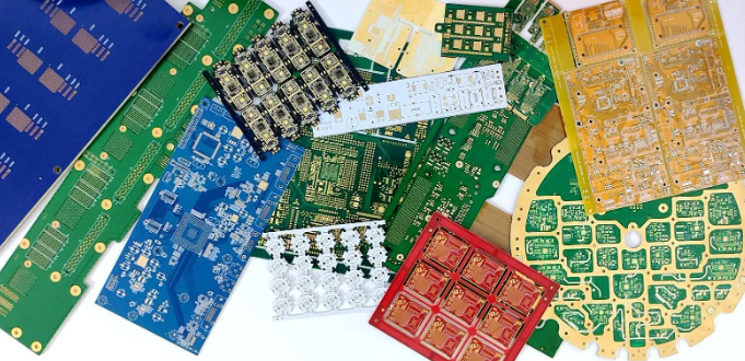
Struggling to find fast, consistent PCB assembly and testing services in Vietnam that meet strict industry standards without long lead times? PCB assembly and testing is the critical final stage of electronic product development, directly impacting product reliability, compliance, and time-to-market for critical applications across medical, aerospace, and industrial equipment sectors. This guide breaks down top local providers, comparison metrics, core processes, quality rules, and practical solutions to streamline your quick-turn PCB projects.
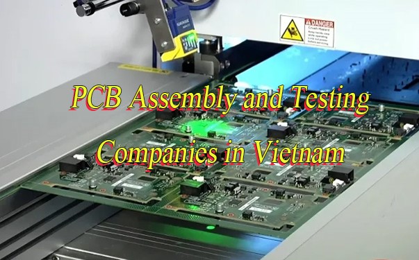
Who Are the Top Quick-Turn PCB Assembly and Testing Companies in Vietnam?
| Company Name | Business Services | Process Capabilities | Standard Quick-Turn Lead Time |
| Best Technology | Quick-turn PCB assembly and testing, prototype PCBA, high-mix low-volume production, DFM analysis, RoHS-compliant assembly, medical & aerospace grade PCBA testing, conformal coating | SMT assembly (01005 components), BGA/QFN/CSP soldering, AOI, ICT, FCT, X-ray inspection, thermal cycling testing, 1-32 layer PCB support, IPC-A-610 Class 3 compliant | Prototypes: 2–5 days; Low-volume production: 7–10 days |
| Vietnam PCB Solutions JSC | Quick-turn PCB assembly, functional testing, industrial equipment PCBA, batch testing, reverse engineering support, DFM review | SMT & through-hole assembly, automated optical testing, in-circuit testing, environmental testing, industrial control PCB specialization, 1-20 layer PCB support | Prototypes: 3–6 days; Small batches: 8–12 days |
| Saigon Electronics Manufacturing Co., Ltd. | Fast-turn PCB assembly and testing solution, aerospace component assembly, medical device PCBA, quality assurance testing, rework services | High-precision SMT, BGA rework, functional load testing, insulation resistance testing, IPC-A-610 compliant, 1-24 layer PCB support | Prototypes: 3–7 days; Mid-volume: 10–14 days |
| Hanoi Quick PCBA | Express PCB assembly, rapid testing, prototype validation, low-cost quick-turn services for industrial and commercial electronics | SMT assembly, basic AOI testing, continuity testing, manual inspection, 1-16 layer PCB support, standard & high-density PCB assembly | Simple prototypes: 1–3 days; Standard batches: 5–8 days |
| Danang PCB Assembly & Test | Quick-turn PCBA, prototype testing, automotive & industrial PCB assembly, RoHS compliance, small-batch quick production | SMT placement, through-hole soldering, AOI, basic functional testing, 1-18 layer PCB support, lead-free assembly | Prototypes: 2–4 days; Small batches: 6–9 days |
| Vina PCB Tech | Quick-turn PCB assembly and testing, medical PCBA prototyping, industrial control board assembly, full test reporting | Micro-component SMT, BGA soldering, X-ray inspection, ICT/FCT testing, 1-28 layer PCB support, ISO 9001 certified | Prototypes: 3–5 days; Low-volume: 8–11 days |
| Binh Duong Electronics Assembly | Fast PCB assembly, quick testing, consumer & industrial electronics PCBA, prototype to mass production transition | SMT & through-hole assembly, AOI testing, continuity checks, 1-16 layer PCB support, high-mix production | Prototypes: 2–5 days; Batches: 7–12 days |
| Hochiminh Quick PCBA Services | Express prototype PCB assembly, rapid functional testing, aerospace & medical prototype support, urgent order handling | High-precision SMT, BGA/QFN assembly, AOI, X-ray, basic ICT testing, 1-24 layer PCB support | Simple prototypes: 1–4 days; Complex prototypes: 5–10 days |
| Viet Phu PCB Assembly | Quick-turn PCB assembly, in-house testing, industrial automation PCBA, lead-free assembly, DFM optimization | SMT assembly, through-hole soldering, functional testing, AOI inspection, 1-20 layer PCB support, IPC-A-610 Class 2 compliant | Prototypes: 3–6 days; Batches: 9–13 days |
| Can Tho Electronics Test & Assembly | Rapid PCB assembly, quick testing services, commercial & light industrial PCBA, small prototype batches | Standard SMT assembly, manual testing, continuity checks, 1-12 layer PCB support, cost-effective quick solutions | Prototypes: 2–4 days; Batches: 6–10 days |
| Vietnam Advanced PCBA | High-speed PCB assembly and testing, medical & aerospace grade PCBA, full compliance testing, prototype validation | Fine-pitch SMT, BGA/CSP assembly, X-ray, ICT, FCT, thermal testing, 1-32 layer PCB support, ISO 13485 aligned | Complex prototypes: 4–7 days; Low-volume: 10–15 days |
| Hai Phong PCB Assembly | Quick-turn industrial PCB assembly, functional testing, marine & heavy equipment PCBA, urgent batch production | SMT & through-hole assembly, AOI, environmental testing, 1-18 layer PCB support, rugged PCB assembly | Prototypes: 3–5 days; Batches: 8–12 days |
| Saigon Quick Tech PCB | Express PCB assembly and testing solution, prototype PCBA, consumer electronics assembly, quick rework services | SMT placement, basic testing, BGA touch-up, 1-16 layer PCB support, fast-track prototype lines | Simple prototypes: 1–3 days; Batches: 5–9 days |
| Viet Nam PCB Assembly Center | Quick-turn PCB assembly, comprehensive testing, industrial & medical PCBA, full quality documentation | SMT/through-hole assembly, AOI, ICT, FCT, X-ray inspection, 1-26 layer PCB support, ISO 9001 certified | Prototypes: 3–6 days; Low-volume: 9–14 days |
| An Giang Electronics PCBA | Affordable quick-turn PCB assembly, basic testing services, small commercial & industrial prototypes, urgent small orders | Standard SMT assembly, manual optical testing, continuity testing, 1-14 layer PCB support | Prototypes: 2–5 days; Batches: 7–11 days |
How to Compare Quick-Turn PCB Assembly and Testing Providers in Vietnam?
Comparing quick-turn PCB assembly and testing providers means focusing on actionable, data-backed factors that directly control project speed, defect rates, and compliance for critical electronic builds. Below are 6 practical criteria to evaluate and rank reliable providers, with clear benchmarks to avoid unqualified partners and keep tight project timelines on track.
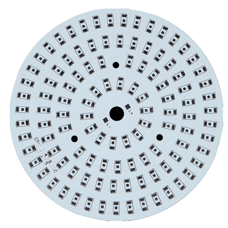
- Check Dedicated Quick-Turn Production Capacity & Allocation: Top quick-turn providers reserve 25-30% of total production capacity exclusively for urgent PCB assembly and testing orders, using separate flexible lines to avoid scheduling conflicts with high-volume mass production. Verify they can support your PCB layer count (up to 32 layers for high-density builds) and micro-component sizes (01005, BGA/QFN) without slowing turnaround, a key marker of specialized quick-turn expertise.
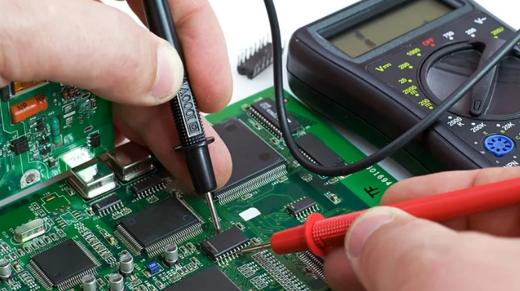
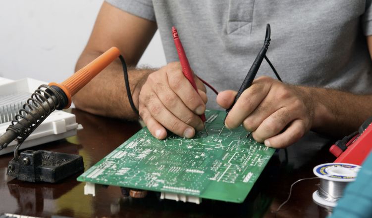
- Audit In-House Testing Equipment & Coverage Rate: Avoid providers that outsource core testing, as this adds 2-3 business days to lead times. Qualified partners have full in-house testing setups, with 100% automated optical inspection (AOI) for standard builds and X-ray inspection for all BGA/CSP assemblies. For medical and aerospace projects, confirm on-site ICT, FCT, and environmental testing to eliminate external delays and ensure full quality coverage.
- Validate Industry Certifications & Defect Rate Benchmarks: Cross-check mandatory certifications: IPC-A-610 Class 3 (high-reliability), ISO 9001, ISO 13485 (medical), and AS9100 (aerospace). Trusted providers maintain a defect rate below 0.5% for quick-turn assemblies, far lower than the industry average of 2% for non-specialized shops. Low, verified defect rates mean less rework and faster project completion.
- Verify Lead Time Consistency & On-Time Delivery Rate: Ignore advertised fast timelines and ask for 90+ day on-time delivery rate data; top providers hit a 98% or higher on-time rate for quoted quick-turn lead times. Request lead time records for projects matching your complexity (prototype, low-volume, high-density) to confirm consistency, as unreliable partners often miss deadlines by 3-5 days for urgent orders.
- Evaluate Free DFM Analysis & Error Prevention Rate: Expert PCB assembly and testing providers offer free, in-depth Design for Manufacturing (DFM) analysis that catches 85-90% of pre-production design flaws before assembly starts. This critical step eliminates assembly errors, testing failures, and costly rework that can derail quick-turn timelines, making DFM support a non-negotiable feature for reliable partners.
- Review Component Sourcing & Traceability Compliance: Component shortages cause 40% of quick-turn project delays, so prioritize providers with authorized global component distributor partnerships and a safety stock of 200+ critical high-demand parts. For medical and aerospace projects, confirm full component traceability for every batch, a mandatory requirement to meet regulatory standards and avoid counterfeit parts.
What Does Best PCB Assembly and Testing Services in Vietnam Include?
Top-tier PCB assembly and testing services go beyond basic soldering and inspection; they deliver end-to-end quality and reliability tailored to industry-specific needs, especially for medical, aerospace, and industrial equipment.
- Comprehensive DFM Analysis: Pre-production design review to optimize PCB layout for quick assembly, minimize component conflicts, and eliminate testing failures. Critical for high-density medical and aerospace PCBs.
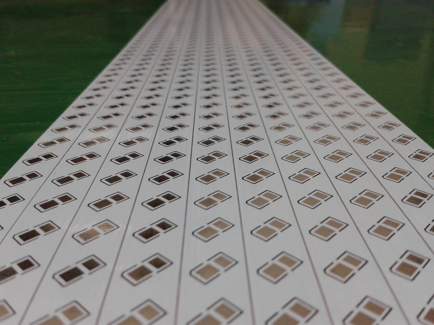
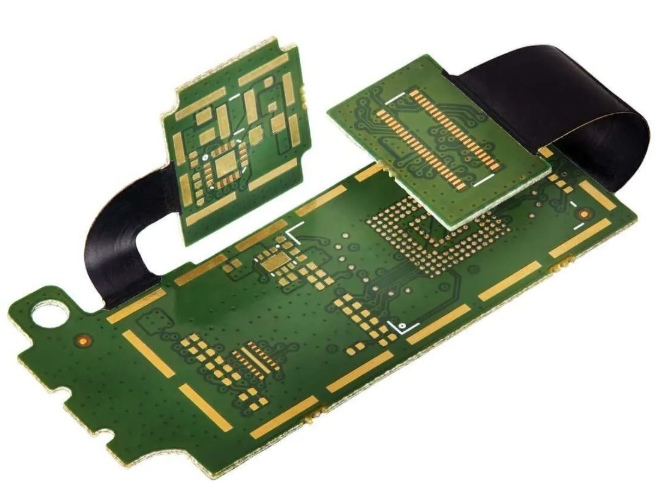
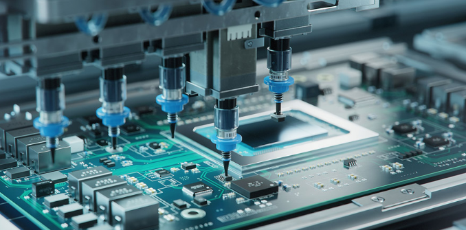
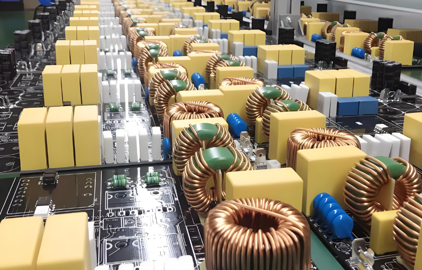
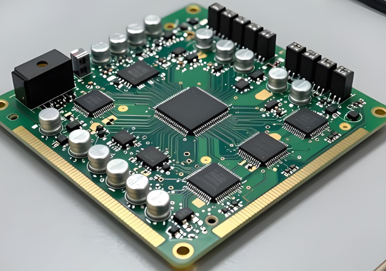
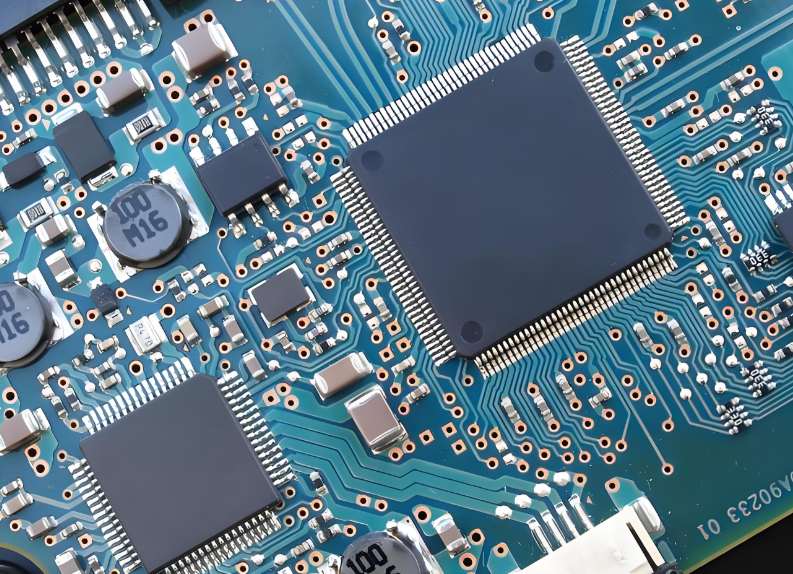
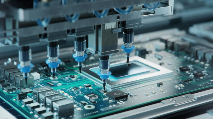
- Precision Component Assembly: Automated SMT placement for micro-components, BGA/QFN soldering with X-ray verification, and through-hole assembly for heavy industrial components, with strict solder joint quality control.
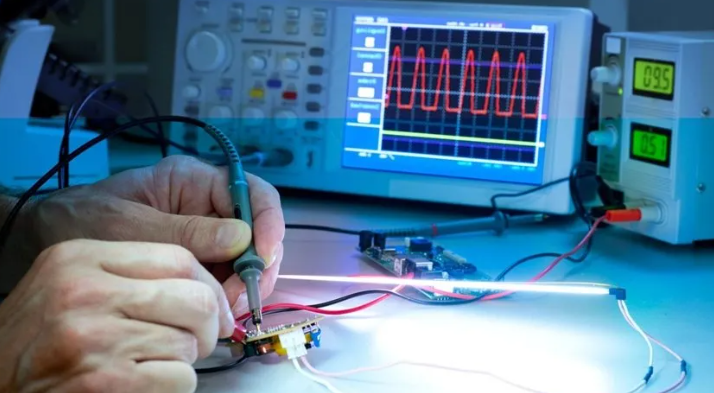
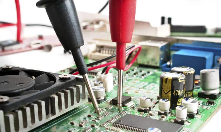
- Multi-Stage Testing Protocol: Sequential testing including AOI (automated optical inspection), ICT (in-circuit testing), FCT (functional circuit testing), and specialized environmental testing for harsh industrial or medical use cases.
- Full Quality Documentation: Detailed test reports, material certificates, and compliance documents for audit and regulatory purposes, mandatory for medical device and aerospace PCB projects.
- Rapid Rework & Repair: In-house rework for defective assemblies without extending lead times, ensuring quick turnaround even if minor issues are detected during testing.
- Industry-Specific Customization: Tailored processes for medical PCBs (sterilization-compatible assembly), aerospace PCBs (vibration resistance testing), and industrial PCBs (high-temperature tolerance validation).
What Are the Process of Quick-Turn PCB Testing and Assembly?
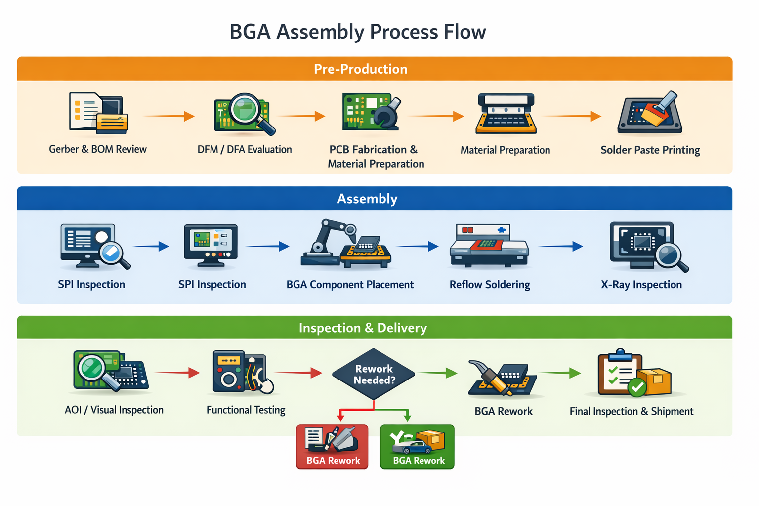
Quick-turn PCB assembly and testing follows a streamlined, optimized workflow to cut lead times without sacrificing quality. Each step is tightly scheduled to eliminate bottlenecks, with parallel processing for testing and assembly where possible.
- Order Confirmation & DFM Check: Within 24 hours of order placement, the team reviews PCB files, BOM, and testing requirements, completes DFM analysis, and confirms production feasibility.
- Material Sourcing & Preparation: Quick access to certified electronic components; priority sourcing for critical parts to avoid delays, with incoming component inspection to verify authenticity.
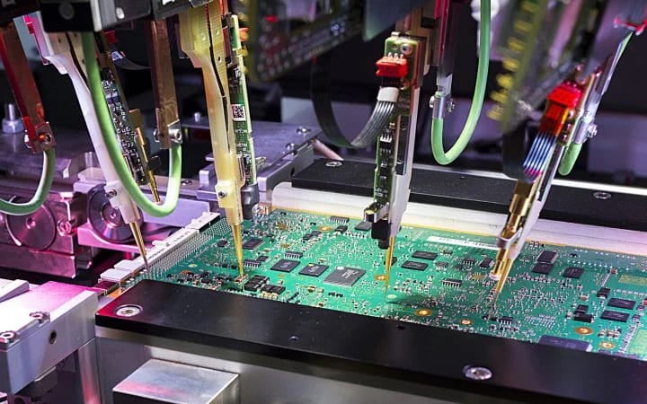
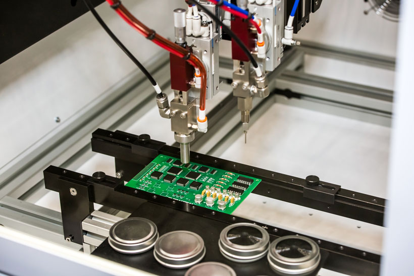
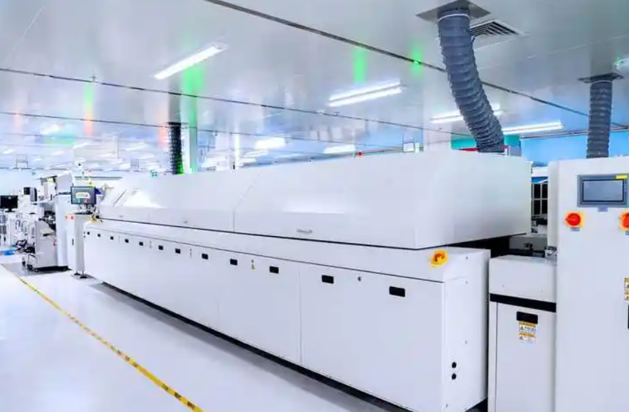
- SMT & Through-Hole Assembly: Automated solder paste printing, component placement, and reflow soldering for SMT parts; manual or wave soldering for through-hole components, with real-time process monitoring.
- First Article Inspection (FAI): Initial inspection of the first assembled PCB to verify alignment, solder quality, and component placement before full batch production.
- Integrated Testing Phase: Sequential AOI, X-ray (for BGA), ICT, and FCT testing; custom functional testing for medical/aerospace applications to validate real-world performance.
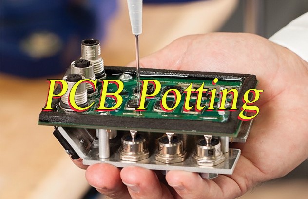
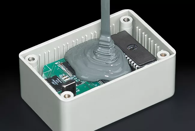
- Cleaning & Conformal Coating (Optional): Precision cleaning to remove flux residues; conformal coating for industrial and outdoor PCBs to protect against moisture and dust.
- Final Inspection & Packaging: Full batch quality check, packaging with ESD protection, and prompt shipping to meet quick-turn deadlines.
What Are the Quality Standards for PCB Assembly and Testing in Vietnam?
Adhering to global quality standards is non-negotiable for PCB assembly and testing, especially for high-reliability industries. These standards ensure consistent performance, durability, and regulatory compliance across all quick-turn projects.
- IPC-A-610 Class 2/3: The primary industry standard for PCB assembly acceptability; Class 2 for general electronics, Class 3 for high-reliability medical, aerospace, and industrial equipment applications.
- IPC-TM-650: Standard testing methods for PCB and PCBA validation, covering solder strength, electrical conductivity, and environmental resistance testing.
- ISO 9001: Quality management system standard ensuring consistent process control, documentation, and continuous improvement in PCB assembly and testing.
- ISO 13485: Medical device quality standard for PCBs used in diagnostic equipment, patient monitoring devices, and other critical medical electronics.
- AS9100D: Aerospace quality standard for PCBs used in avionics, satellite systems, and aerospace control equipment, requiring extreme reliability and traceability.
- RoHS & REACH: Environmental compliance standards restricting hazardous materials, mandatory for global market distribution of assembled PCBs.
How Long Does Quick-Turn PCB Assembly and Testing in Vietnam Take?
Quick-turn PCB assembly and testing lead times vary based on PCB complexity, layer count, component type, and testing requirements. Below is a realistic timeline breakdown for common project types in Vietnam.
| Order Quantity (Pieces) | PCB Complexity Level | Standard Testing Included | Typical Quick-Turn Lead Time (Business Days) |
| 1 – 20 PCS (Prototype Sample) | Basic: 1-4 layers, standard SMT components, no BGA/QFN | 100% AOI + continuity testing | 1 – 3 days |
| 21 – 100 PCS (Small Prototype Batch) | Medium: 4-16 layers, mixed SMT, optional BGA/QFN | AOI + X-ray (for BGA) + basic ICT testing | 3 – 5 days |
| 101 – 500 PCS (Low-Volume Production) | High: 8-24 layers, fine-pitch SMT, BGA/QFN/CSP components | Full AOI, X-ray, ICT, FCT, visual quality inspection | 6 – 9 days |
| 501 – 1000 PCS (Mid-Volume Quick Build) | Advanced: 12-32 layers, high-density interconnect (HDI), specialized components | Full test suite + first article inspection (FAI) report | 9 – 12 days |
How Much Does Printed Circuit Board Assembly in Vietnam and Testing Cost?
For quick-turn PCB assembly and testing in Vietnam, typical pricing ranges from $25 to $350 per order, with prototype orders falling at the lower end and high-complexity, low-volume production orders landing at the higher end. This range reflects standard quick-turn services, excluding specialized testing or rare component premiums, and aligns with local Vietnam manufacturing market rates for fast-turn PCBA projects.
Order Quantity is the primary cost driver for PCB assembly and testing. Small prototype batches (1-20 pieces) carry higher per-unit costs due to fixed setup and testing fees, while larger low-volume batches (101-500 pieces) lower per-unit costs via economies of scale, even with full testing included. Setup fees account for 30-40% of total prototype costs, making quantity the biggest variable in final pricing.
PCB Complexity & Component Type directly impacts total cost. Basic 1-4 layer PCBs with standard SMT components cost far less than high-density 12-32 layer boards with BGA/QFN/CSP micro-components. Fine-pitch assembly, X-ray inspection for BGAs, and specialized component handling add 15-35% to baseline costs, as they require more precise equipment and skilled labor.
Testing Scope & Compliance Requirements also alter pricing. Basic AOI and continuity testing is included in standard quick-turn rates, but advanced testing (ICT, FCT, thermal cycling, environmental testing) and industry compliance (IPC Class 3, ISO 13485, AS9100) add incremental costs. Full regulatory testing and documentation for medical or aerospace use can increase total costs by 20-40% compared to standard testing packages.
Lead Time Speed affects cost as well. Standard quick-turn lead times (2-5 days for prototypes) include baseline rates, while urgent rush orders (24-48 hour turnaround) require priority production scheduling and add 10-25% to total PCB assembly and testing costs, as providers reallocate production capacity to meet tight deadlines.
What Are Common Challenges and Solutions for PCB Assembly and Testing in Vietnam?
Quick-turn PCB assembly and testing faces unique challenges due to tight timelines and high precision demands. Below are the most frequent issues and proven solutions to keep projects on track. Here are common challenges and solutions for PCB assembly and testing:
1. Component Placement Errors
- Challenge: Misaligned SMDs or wrong parts due to human error/poor pick-and-place calibration.
- Solution: Automated optical inspection (AOI) + AI-driven vision systems for real-time correction.
2. Soldering Defects
- Challenge: Poor wetting, voids, or bridging from improper reflow profiles/flux application.
- Solution: Optimized solder paste screening + laser-based reflow monitoring for thermal profiling.
3. Electrical Test Failures
- Challenge: Open/short circuits or impedance mismatches during ICT/flying probe tests.
- Solution: Pre-test simulation (e.g., SPICE) + boundary scan (JTAG) for in-circuit validation.
4. Thermal Management Issues
- Challenge: Hotspots causing component failure or delamination under power cycles.
- Solution: Thermal imaging + finite element analysis (FEA) for heat sink/copper trace optimization.
5. Signal Integrity Problems
- Challenge: Crosstalk/EMI from high-speed traces or poor grounding.
- Solution: Time-domain reflectometry (TDR) + impedance-controlled stackup design.
6. Environmental Stress Failures
- Challenge: Humidity/temperature extremes causing corrosion or material expansion.
- Solution: Conformal coating + HALT/HASS testing for accelerated lifecycle validation.
FAQs About PCB Assembly and Testing Service in Vietnam
Q1: What’s the difference between standard and quick-turn PCB assembly and testing?
A1: Quick-turn PCB assembly and testing uses dedicated flexible production lines, priority scheduling, and streamlined processes to deliver projects in days instead of weeks, while standard assembly follows regular batch timelines. Quick-turn services prioritize speed without cutting quality corners, ideal for prototype and urgent production needs, and often include expedited DFM and testing for medical and industrial projects.
Q2: Can quick-turn PCB assembly support BGA and high-density components?
A2: Yes, top quick-turn providers in Vietnam are equipped with high-precision SMT machines and X-ray inspection to handle BGA, QFN, and micro-components (01005 size). They follow strict IPC Class 3 standards for soldering and testing, ensuring reliable performance for high-density PCBs used in aerospace and medical devices.
Q3: Do quick-turn PCB assembly services include full testing for medical applications?
A3: Reputable providers offer customized testing for medical PCBs, including functional testing, insulation resistance testing, and sterilization-compatible validation, alongside ISO 13485 compliance. Full test reports and traceability documentation are provided to meet medical regulatory requirements.
Q4: How to ensure quick-turn PCB assembly meets aerospace quality standards?
A4: Choose providers with AS9100 certification, in-house X-ray and thermal cycling testing, and full component traceability. They follow strict process controls for aerospace PCBs, conduct first-article inspection for every batch, and provide detailed compliance documentation to meet aviation and aerospace industry requirements.
Q5: What causes delays in quick-turn PCB assembly and testing, and how to avoid them?
A5: Common delays include incomplete design files, component shortages, and unaddressed design flaws. Avoid delays by submitting complete PCB and BOM files upfront, approving DFM changes immediately, and working with providers that have in-house component stock and dedicated quick-turn capacity to minimize hold-ups.