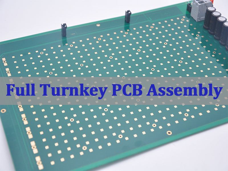
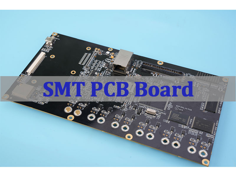
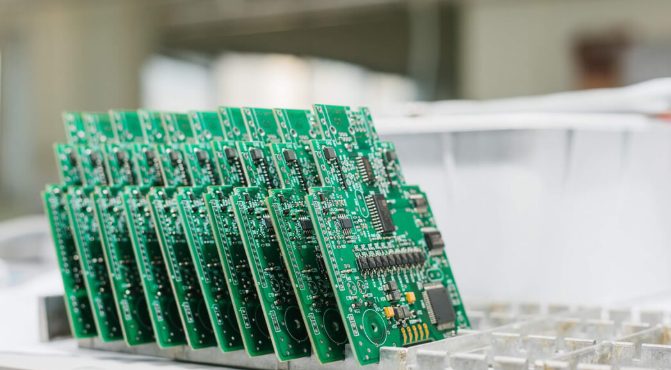
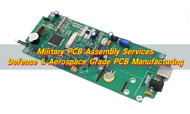
What Is Military PCB Assembly?
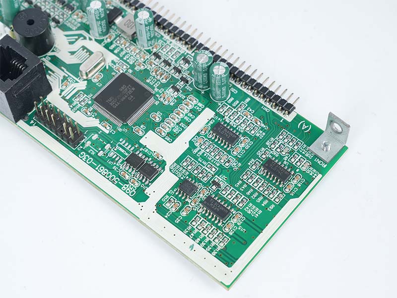
Military PCB assembly refers to the fabrication, component placement, soldering, inspection, and testing of printed circuit boards used in defense and aerospace systems. These boards are designed for harsh conditions and zero-tolerance reliability targets.
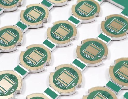
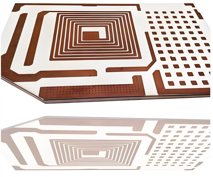
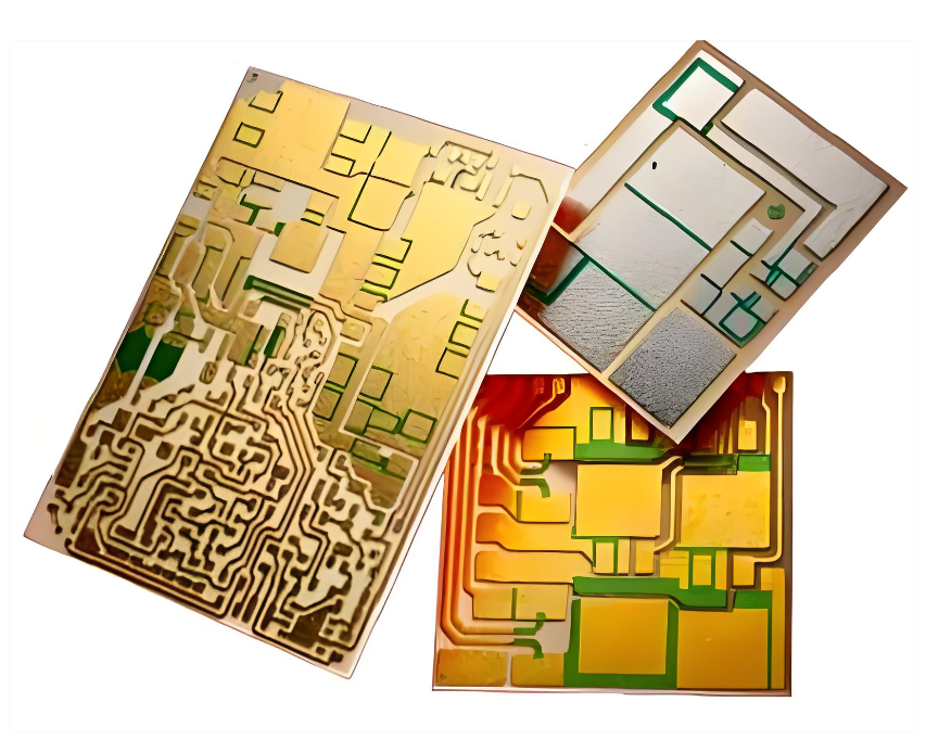
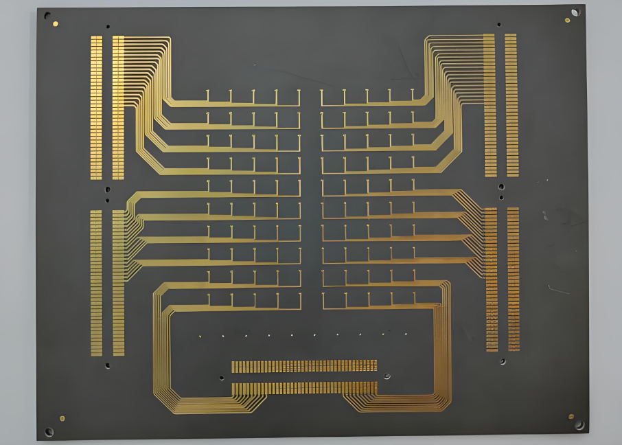
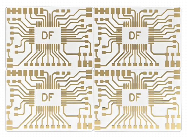
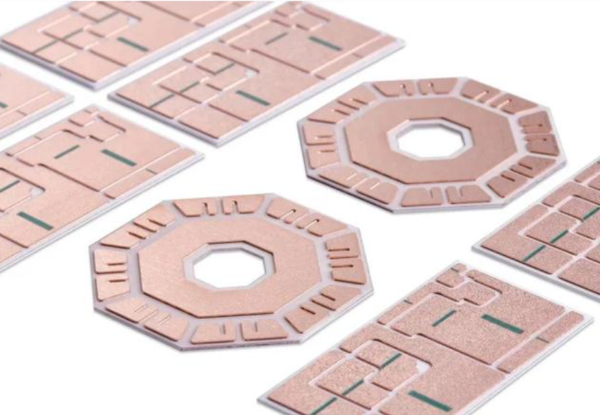
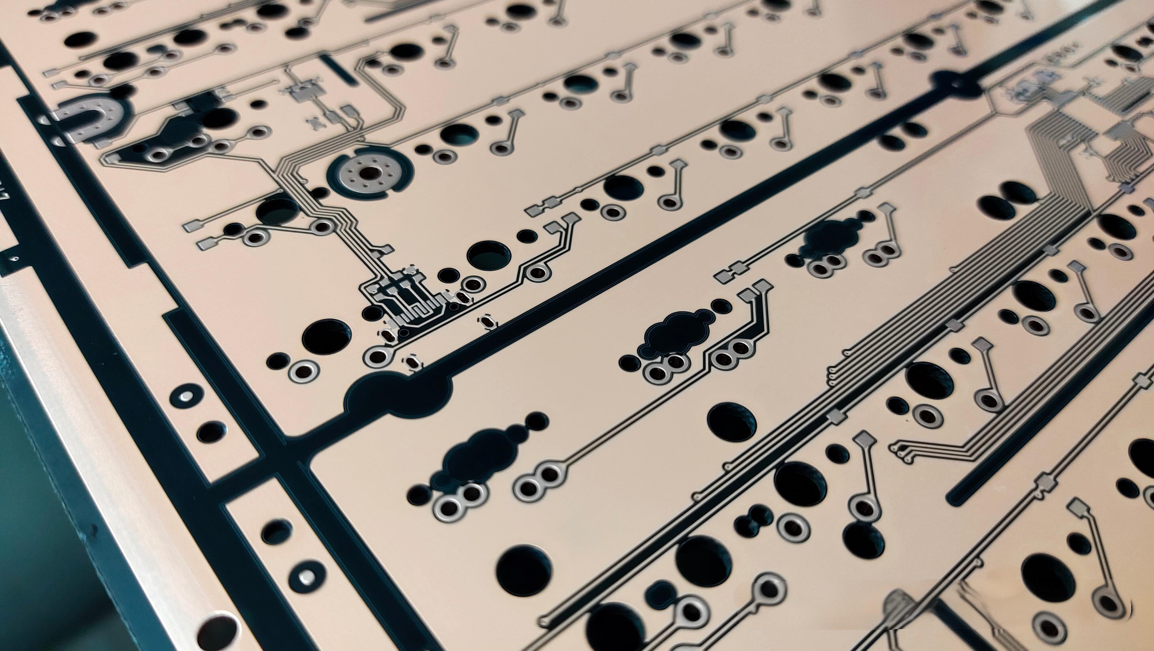
Military assemblies are not defined by a single board type. They can be rigid, HDI, flex, rigid-flex, heavy copper, metal-core, or hybrid builds. What makes them “military-grade” is the discipline applied during manufacturing.
Unlike fast-moving consumer electronics, defense electronics often stay in service for decades. Long-term component availability, repairability, and configuration control matter as much as initial performance.
Military PCB assembly also places strong emphasis on consistency. Each build must match the approved data package. Variations are managed through formal change control, not informal adjustments on the shop floor.
How Is Military PCB Assembly Different from Commercial PCB Assembly?
The difference between military and commercial PCB assembly is not subtle. It affects design rules, materials, inspection depth, documentation, and even factory culture.
Commercial PCB assembly often prioritizes speed and cost. Military programs prioritize certainty and repeatability. Yield is important, but predictability matters more.
Key differences include:
- Quality expectations: Military assemblies usually follow higher acceptance criteria. Solder joints must meet stricter shape and wetting requirements. Cosmetic defects that are acceptable in consumer products may trigger rejection in defense programs.
- Process control: Military PCB assembly relies on documented processes. Profiles, torque values, solder alloys, and cleaning methods are defined and locked. Deviations require formal approval.
- Inspection depth: Visual inspection alone is not enough. AOI, X-ray, micro-sectioning, and electrical tests are common. Some programs require 100% inspection.
- Traceability: Every lot of boards, components, solder paste, and even operators can be traced. This level of traceability supports audits and long service life support.
- Lifecycle mindset: Commercial products may change yearly. Military platforms often remain active for 10, 20, or even 30 years.
Because of these differences, not every PCBA factory can support military work. The gap is not just equipment. It is process discipline and mindset.
Key Terminology for Military PCB Assembly
Understanding military PCB assembly requires fluency in its technical language.
- Class 3 / Class 3A: High-reliability assembly classes that define tighter workmanship requirements.
- Conformal coating: A protective layer applied to assembled boards to resist moisture, dust, and chemicals.
- First Article Inspection (FAI): A detailed verification of the first production unit against design data.
- Lot traceability: The ability to trace materials and processes back to specific production lots.
- Controlled soldering profile: A validated thermal curve used during reflow or wave soldering.
- Configuration control: Formal management of design revisions and process changes.
- Environmental stress screening (ESS): Testing that exposes assemblies to temperature cycling or vibration to reveal latent defects.
What Is the Military Standard for PCB?
There is no single “one-size-fits-all” military PCB assembly standard. Instead, military programs rely on a framework of specifications, industry standards, and customer-specific requirements.
Commonly referenced standards include:
- IPC workmanship and performance standards for high-reliability assemblies
- Military performance specifications that define material and process expectations
- Aerospace quality management systems focused on risk control and traceability
Military PCB assembly standards typically address:
- Solder joint geometry and acceptance criteria
- Material qualification and storage
- Operator training and certification
- Inspection methods and frequency
- Documentation and record retention
Many defense programs also impose program-specific rules. These may include additional testing, tighter cleanliness limits, or unique marking requirements.
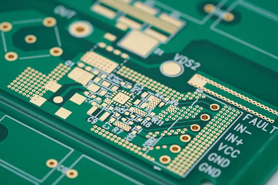
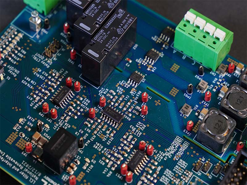
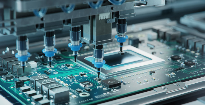
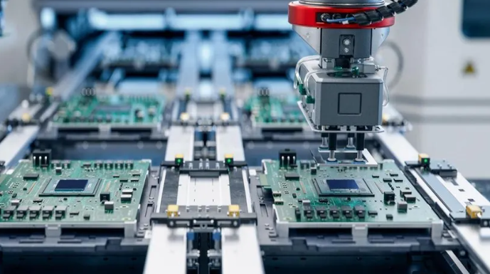
The Precision Manufacturing Process of Military PCB Assembly
Military PCB assembly follows a structured, disciplined manufacturing flow. Each step builds confidence that the final assembly will perform as intended, even in extreme conditions.
- Design review and DFM: The process begins with a deep review of the design data. Stack-ups, land patterns, solder mask openings, and component choices are examined.
- Material and component control: Only approved materials enter production. Components are checked for authenticity and stored under controlled conditions.
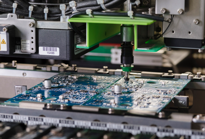
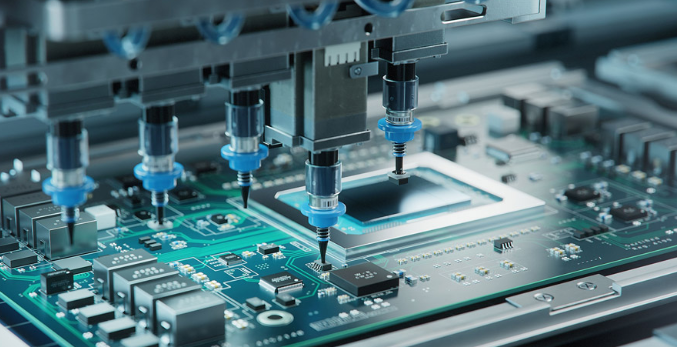
- Solder paste printing and placement: Printing parameters are tightly controlled. Placement machines are programmed for accuracy and repeatability.
- Reflow and selective soldering: Thermal profiles are validated and locked. For mixed technology boards, selective soldering is used to protect sensitive parts.
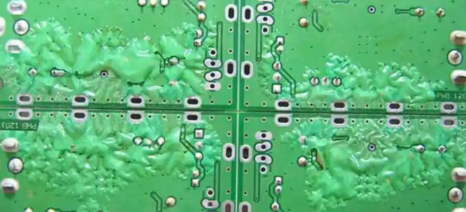
- Cleaning and inspection: Residues are removed when required. Assemblies undergo AOI, X-ray, and skilled visual inspection.
- Coating and protection: When specified, conformal coating or encapsulation is applied. Coverage is verified to ensure protection without interfering with connectors or test points.
- Electrical and functional testing: Continuity, isolation, and functional tests confirm electrical performance.
- Final documentation and release: All records are compiled. Traceability data is confirmed. Only then is the assembly released for delivery.
This structured flow is what separates true military-grade PCB assembly from ordinary production.
How to Choose a Qualified Military PCB Assembly Service Provider?
Selecting the right partner for military PCB assembly is a strategic decision. Price matters, but capability and trust matter more.
A strong service provider demonstrates the following traits:
- Proven experience: Look for a history of defense or aerospace projects. Experience reduces risk.
- Certified quality systems: Certifications alone are not enough, but they indicate a baseline of discipline.
- Process transparency: A reliable provider welcomes audits and technical discussions.
- Engineering support: Early feedback during design review can prevent costly issues later.
- Traceability systems: Digital tracking of materials, processes, and test results is essential.
- Long-term support mindset: Military programs rarely end after one build. The provider should support repeat orders and revisions.
EBest Circuit (Best Technology) supports military-grade PCB assembly with controlled processes, full traceability, and engineering-driven communication. The focus is not only on building boards, but on protecting program reliability over time.
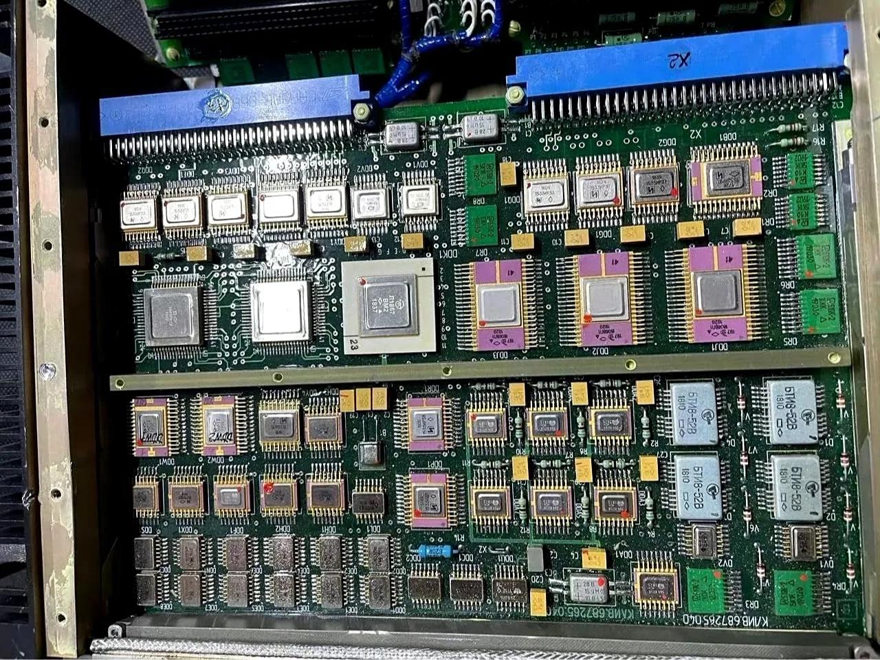
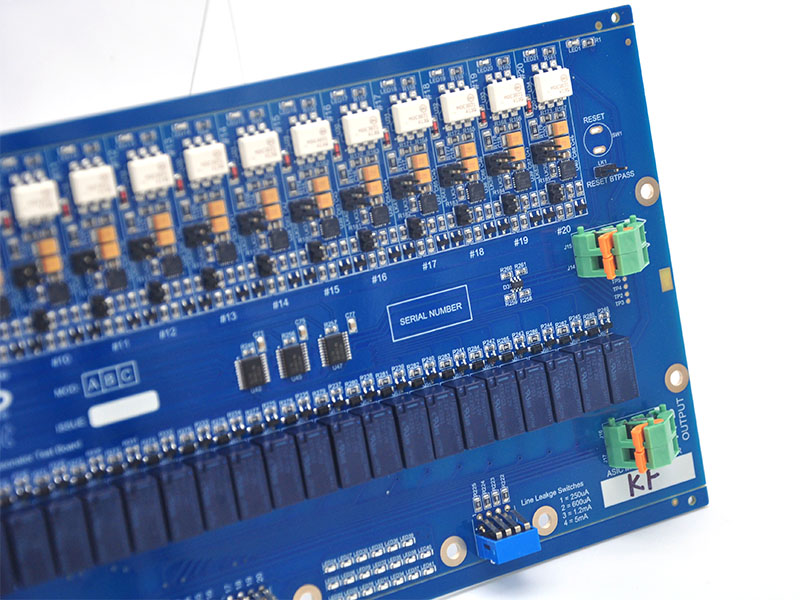
Common Applications of Military PCB Assembly in Defense
Military PCB assembly supports a wide range of defense and aerospace systems. Each application places different demands on design and manufacturing.
Typical applications include:
- Radar and surveillance systems: These boards handle high frequencies and power levels. Signal integrity and thermal management are critical.
- Secure communication equipment: Reliability and electromagnetic control are essential. Assemblies must perform in mobile and fixed environments.
- Avionics and flight control: Weight, reliability, and resistance to vibration define success in airborne systems.
- Guidance and navigation modules: Precision and stability are required. Even minor defects can affect accuracy.
- Electronic warfare systems: Complex architectures and dense layouts demand advanced assembly skills.
Across these applications, failure is not an option. Military PCB assembly provides the foundation that makes these systems dependable.
FAQs About Military PCB Assembly
- Is military PCB assembly always more expensive?
It often costs more than commercial assembly due to inspection depth, documentation, and process controls. However, it reduces long-term risk and rework.
- Can commercial components be used in military PCB assembly?
Sometimes, yes. The decision depends on availability, lifecycle, and program requirements. Risk analysis is key.
- How long does military PCB assembly take?
Lead time varies by complexity and approval cycles. Early planning and clear documentation help avoid delays.
- Is conformal coating always required?
Not always. It depends on the operating environment and system requirements.
- What role does traceability play?
Traceability supports audits, failure analysis, and long-term support. It is a core element of military-grade assembly.
Conclusion:
Military PCB assembly is defined by discipline, not shortcuts. It demands strict process control, skilled operators, validated equipment, and complete traceability. From design review to final test, every step supports long-term reliability in defense and aerospace systems.
If you are planning or supporting a military-grade PCB assembly project, EBest Circuit (Best Technology) provides engineering-driven assembly services that align with military PCB assembly standards. For technical discussion or quotation support, contact sales@bestpcbs.com