What is soldering vs welding? Soldering and welding are both essential techniques used in metal joining processes. However, they are quite distinct in terms of their methods, applications, and results. These processes are often confused, but understanding the differences is crucial, especially when deciding which method to use for various applications.
What is soldering and welding?
Both soldering and welding are techniques used to join metal pieces together, but they operate very differently.
Soldering is a method that uses a filler material, called solder, to join two or more metal parts. The process involves melting the solder, which has a lower melting point than the base materials, and allowing it to solidify, creating a bond between the components.
Unlike welding, which typically involves high heat, soldering works at lower temperatures, making it suitable for more delicate materials like circuit boards and wires.
Welding, on the other hand, involves melting the base metals themselves and allowing them to fuse together. This requires much higher temperatures than soldering.
Welding is often used for structural applications, such as in building construction, automotive, and manufacturing, where strong, durable bonds are required.
Is soldering as strong as welding?
The strength of a soldered joint compared to a welded joint depends on the application. Welding produces much stronger bonds than soldering because it involves the fusion of the base metals.
In contrast, soldering uses a filler metal to create a bond, which is typically weaker than the base metal itself. However, soldering is sufficient for many applications, especially in electronics, plumbing, and small repairs.
How strong is soldering vs welding?
Welding generally creates a stronger, more permanent bond than soldering. The strength of a weld comes from the fact that the base metals are directly melted and fused, which creates a solid, continuous bond.
Soldering, by contrast, is generally not as strong and is usually used for joining metals that don’t need to withstand as much stress. This makes soldering perfect for smaller, more delicate components, such as electrical connections, where excessive strength is not required.
In many electronic applications, soldering provides adequate strength for the components to function reliably, but it won’t hold up as well under heavy mechanical stress compared to welding.
What is welding used for?
Welding is used primarily in industries where strong, durable bonds are needed. These applications include:
- Construction: Welding is essential in the construction of steel structures and buildings.
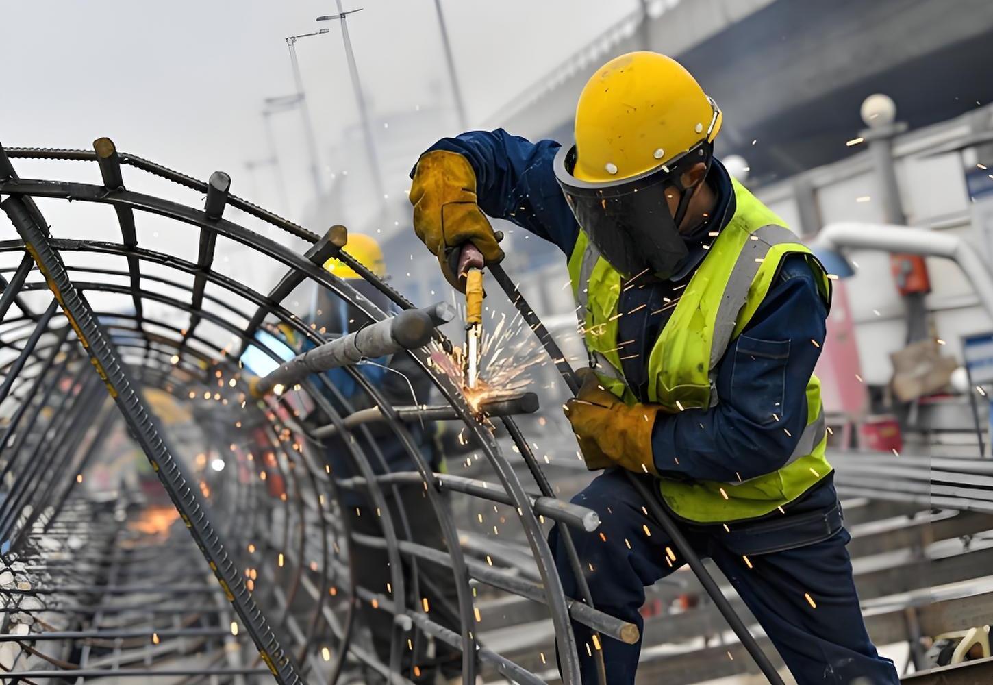
- Automotive: Cars and trucks rely on welding for structural integrity.
- Shipbuilding: Welding is used to join large metal sheets in ship hulls.
- Heavy machinery: Welding helps in creating durable joints in machinery used for construction or mining.
Welding provides a long-lasting, highly durable bond that is necessary for these types of applications.
What are the advantages of soldering over welding?
While welding is stronger in terms of the bond strength, soldering has several advantages that make it ideal for specific applications:
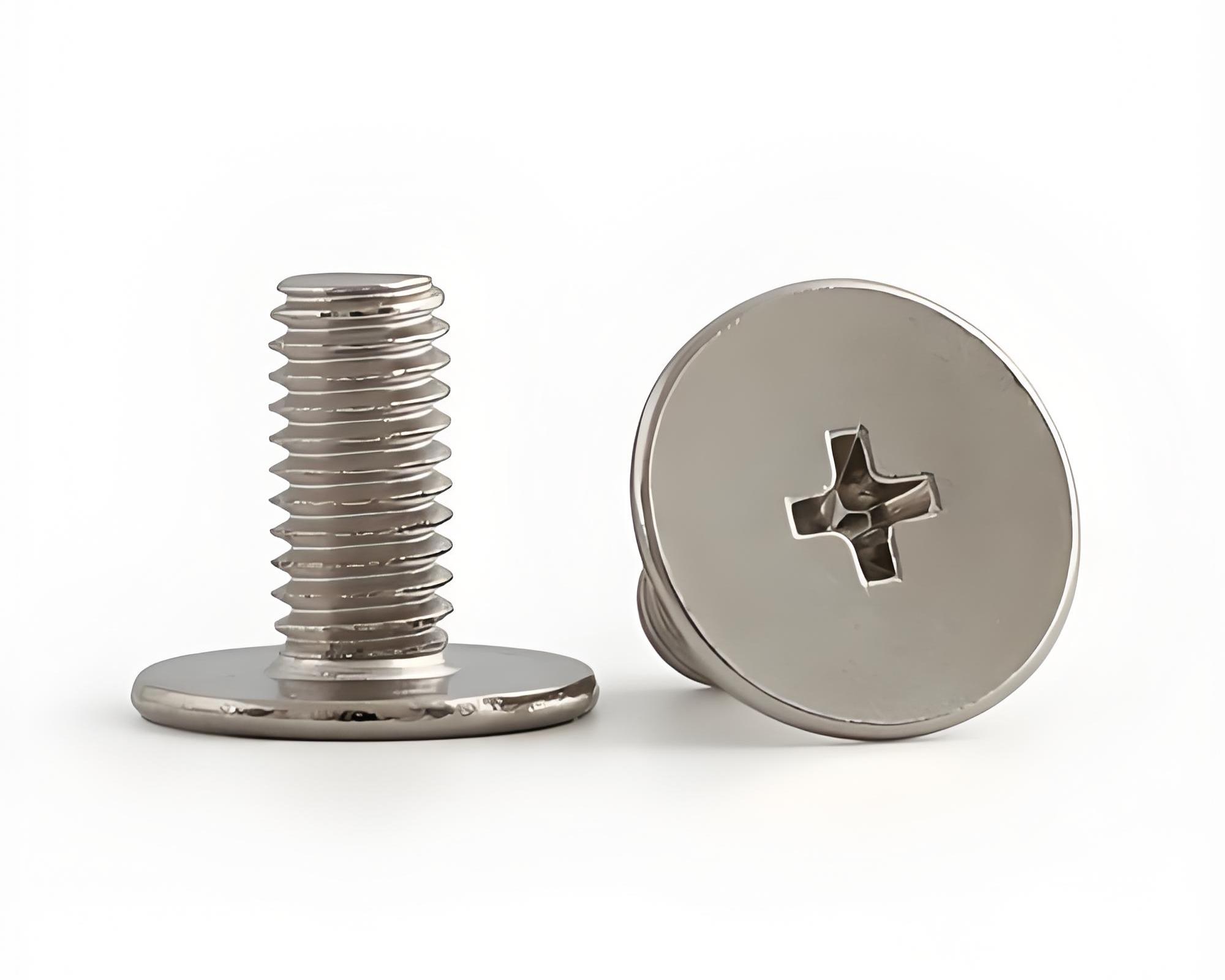
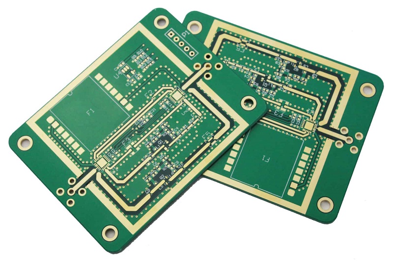
- Lower temperature: Soldering uses a much lower temperature than welding. This makes it suitable for delicate electronic components, such as PCBs, that could be damaged by the high heat of welding.
- Ease of use: Soldering is generally easier and faster than welding, especially for small, intricate jobs.
- No need for high-powered equipment: Unlike welding, which requires heavy machinery, soldering can be performed with simple tools like a soldering iron or soldering gun.
- Cost-effective: Since soldering uses a lower heat and simpler tools, it’s typically more affordable than welding.
- Precision: Soldering allows for more precise, controlled work. This makes it ideal for small, delicate tasks, such as joining electronic components on a PCB.
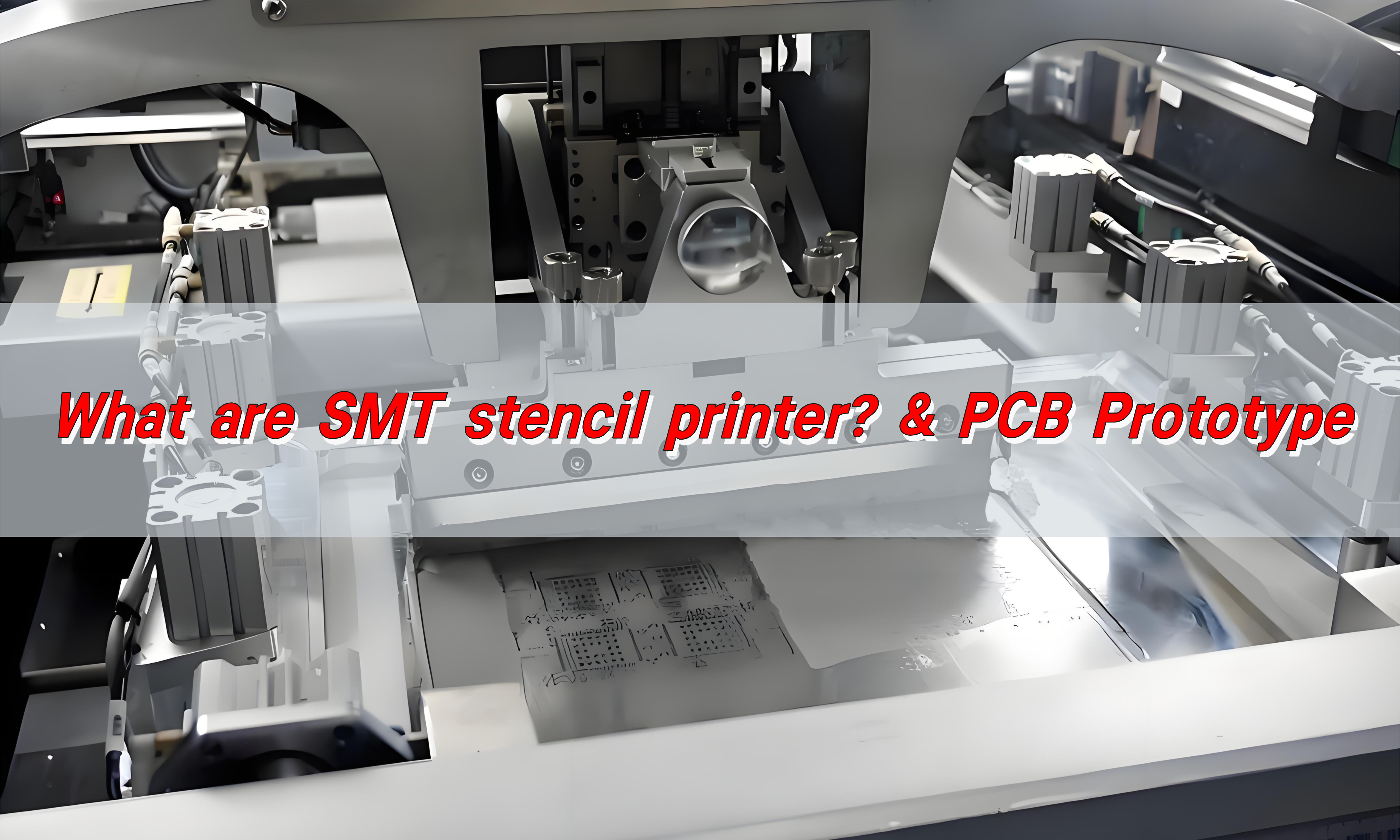
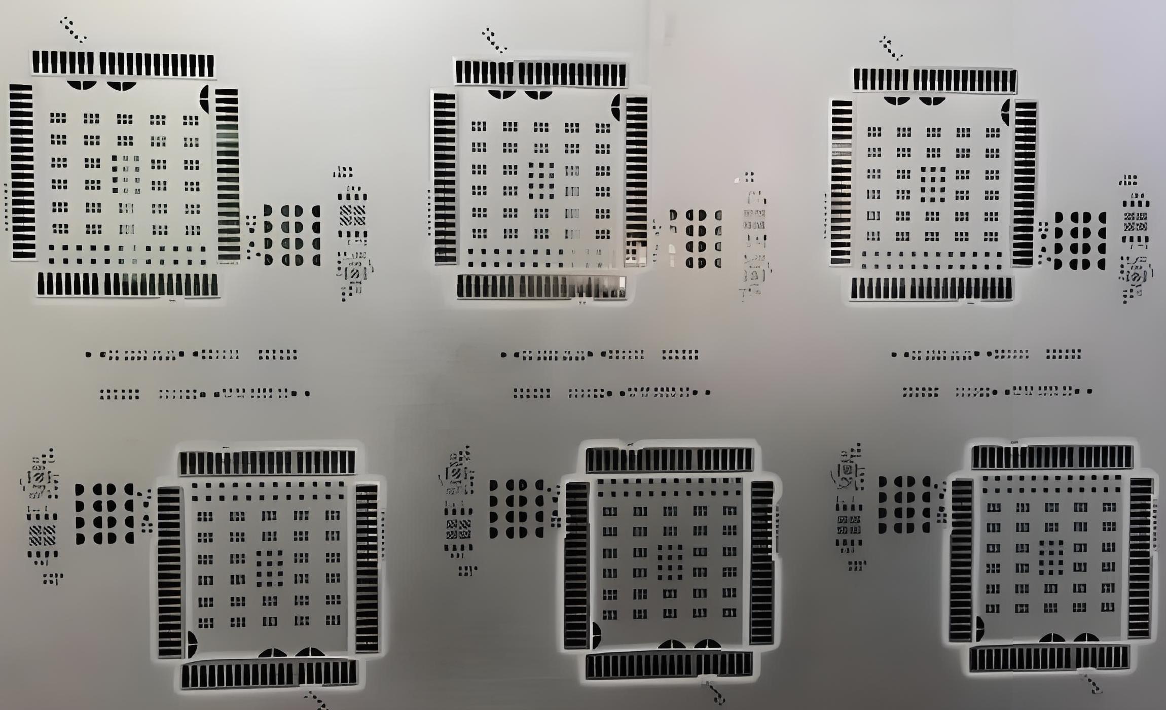
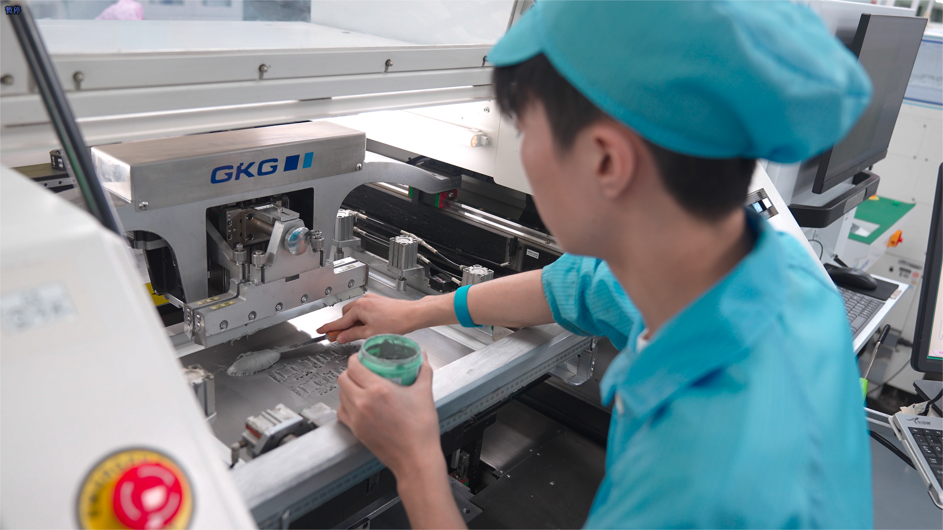
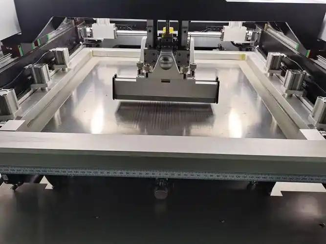
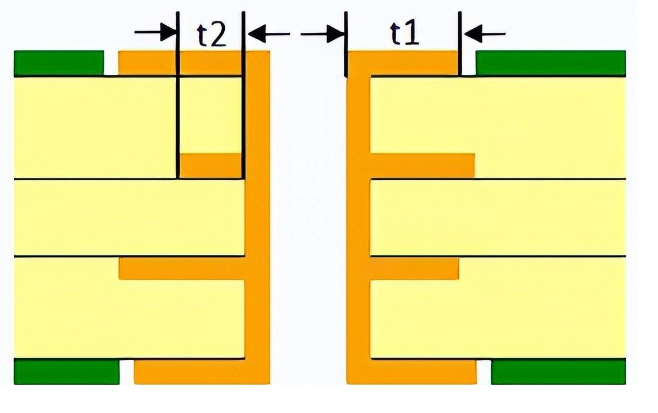
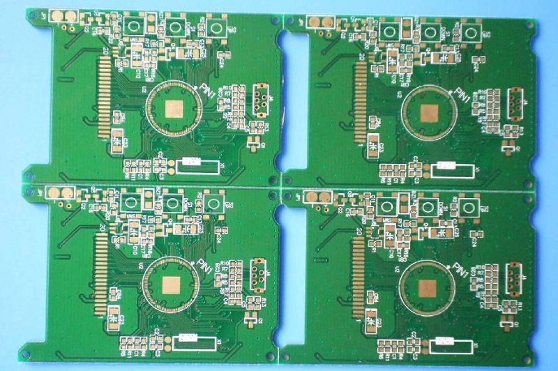
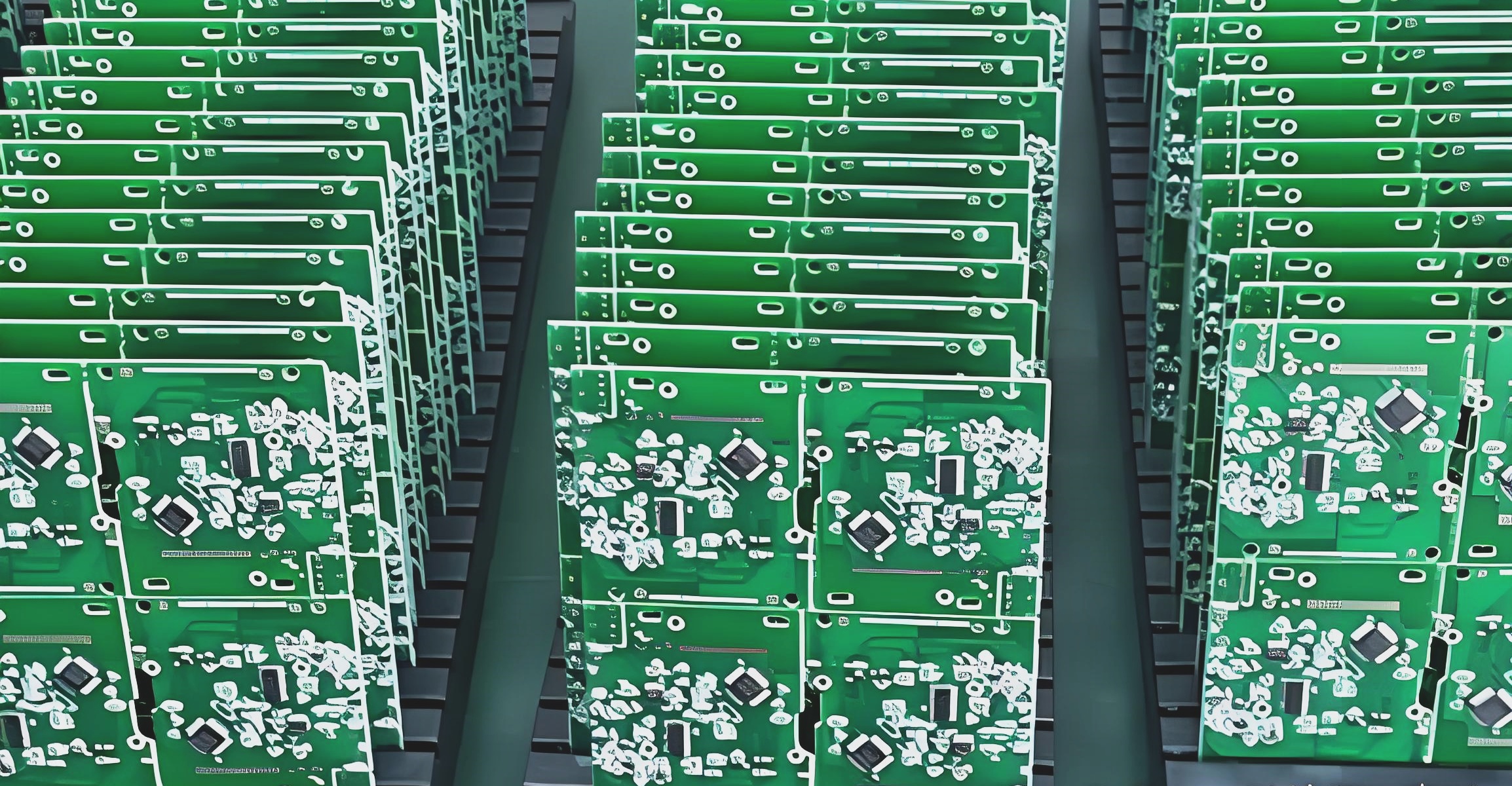
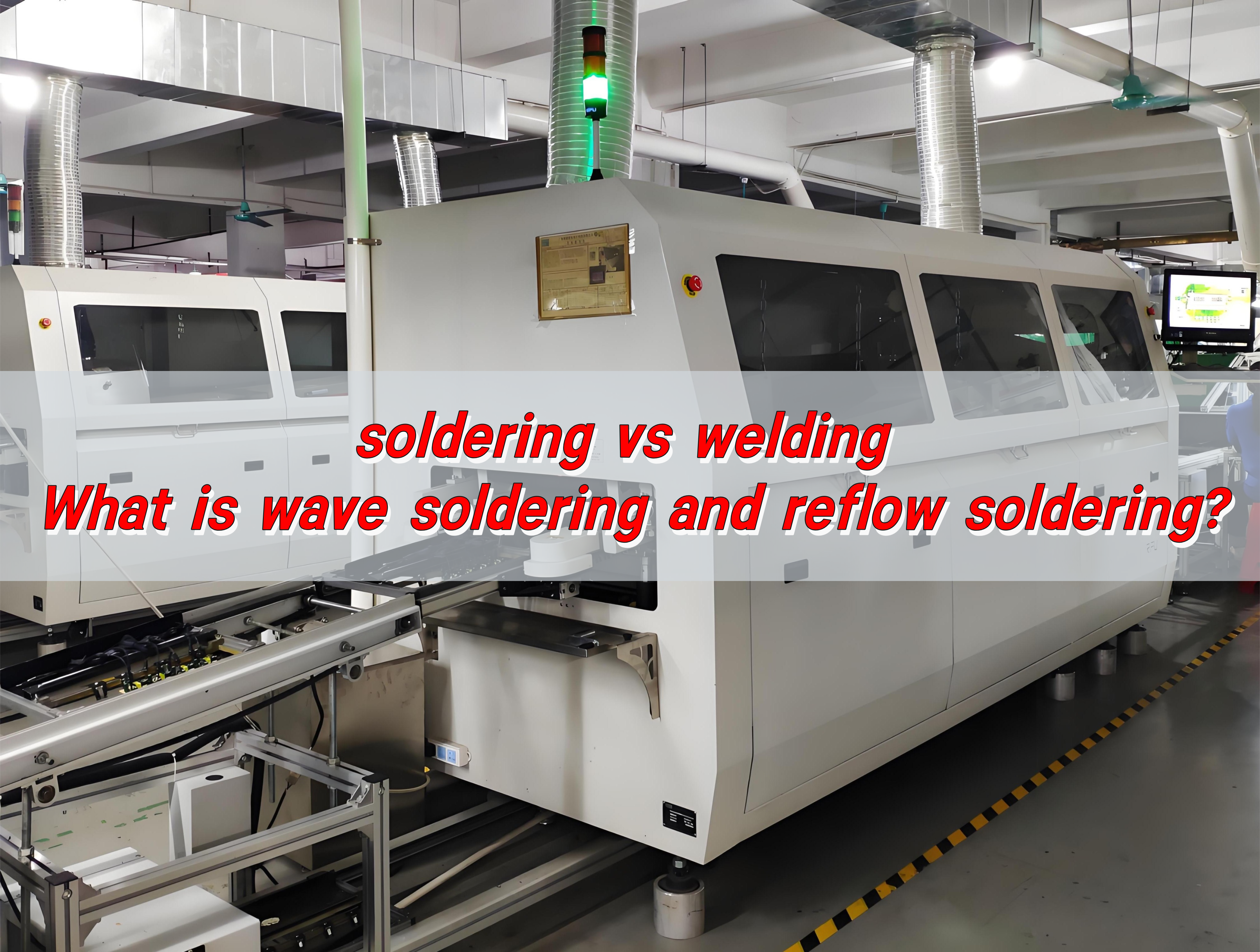
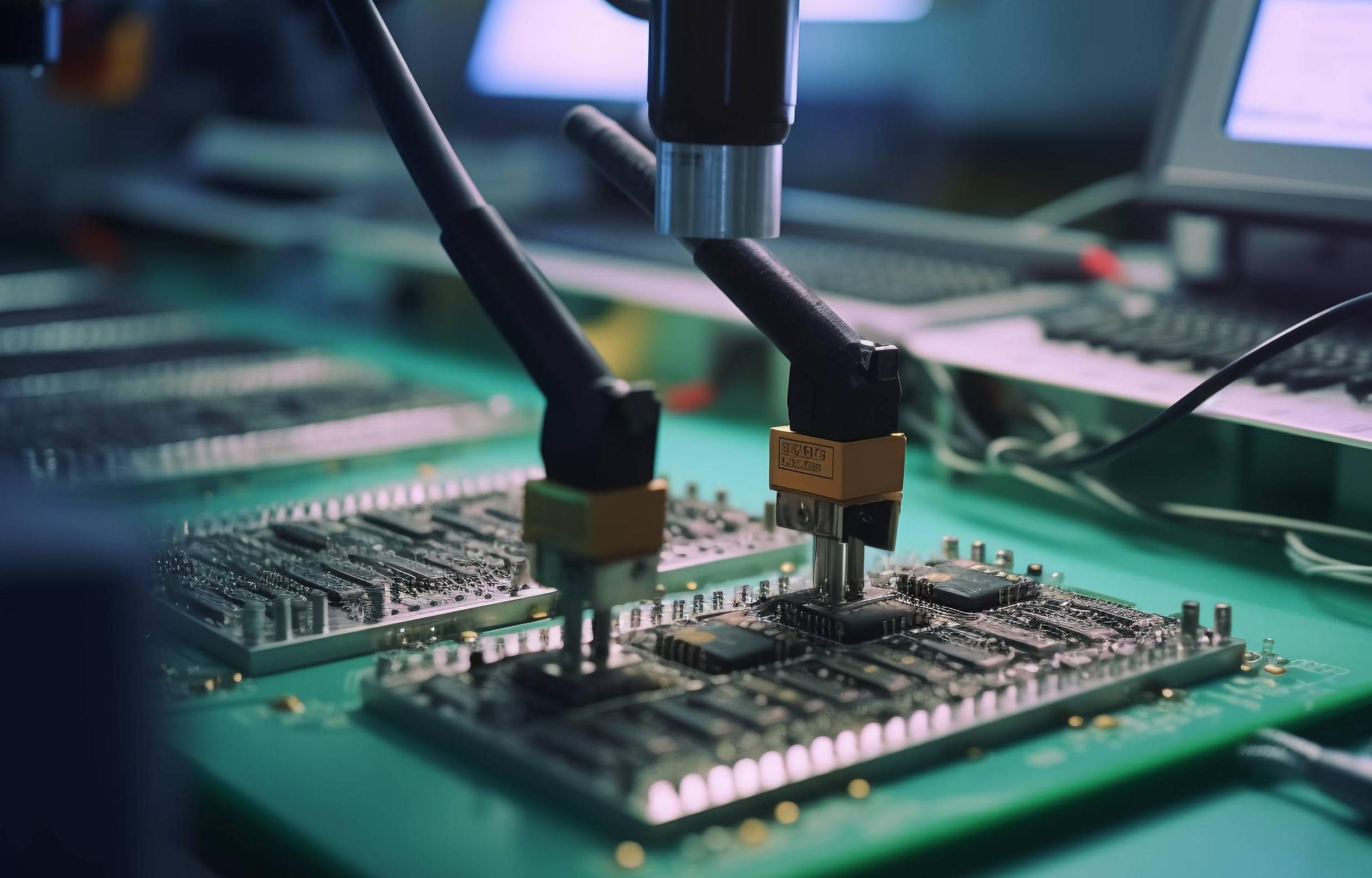
What is wave soldering and reflow soldering?
Both wave soldering and reflow soldering are specialized soldering techniques used primarily in electronics manufacturing, especially for PCBs.
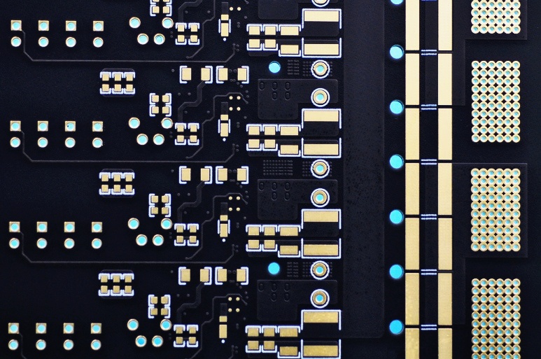
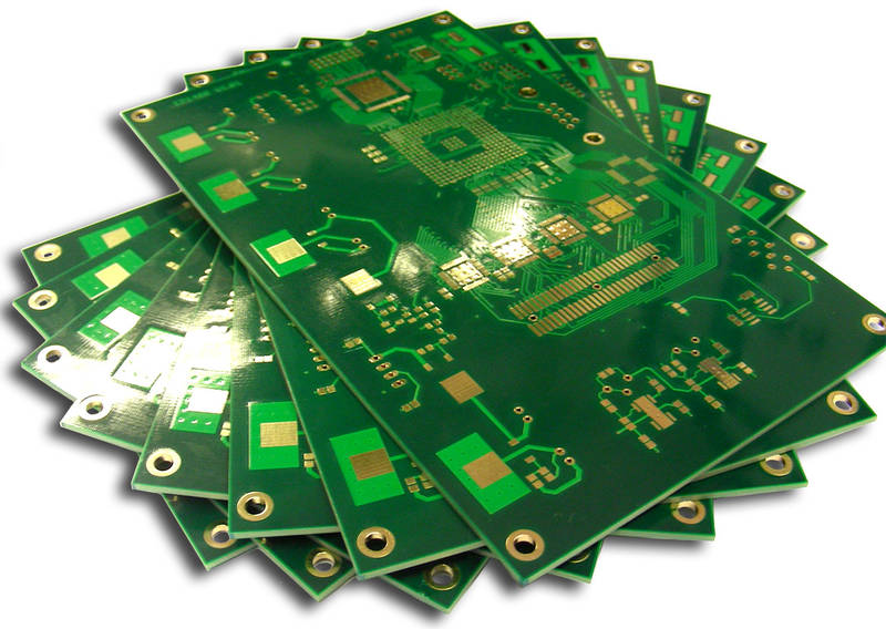
Wave Soldering: This is a process where a PCB is passed over a wave of molten solder. The solder waves are carefully controlled to ensure that the solder adheres to the joints of the components. Wave soldering is often used for large quantities of boards that require consistent results. This process is ideal for through-hole components, where leads need to be soldered into the PCB.
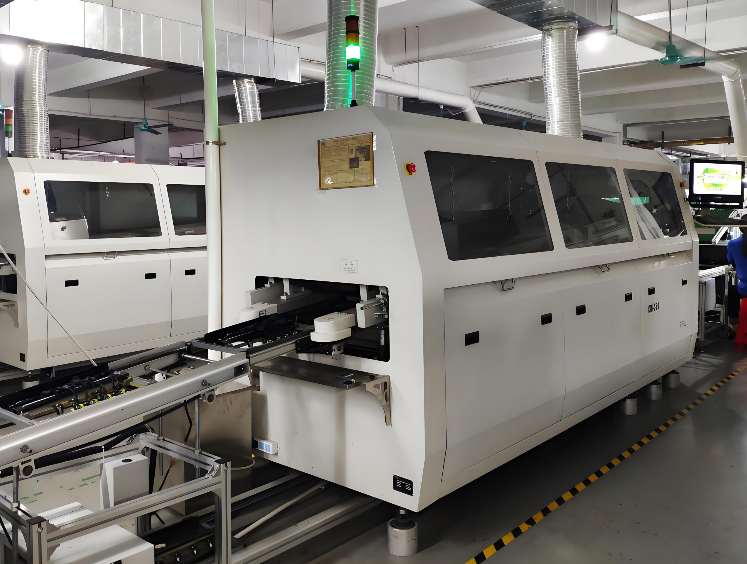
Reflow Soldering: This technique is used primarily for SMD (Surface-Mounted Devices). The process involves applying solder paste to the PCB, placing the components, and then heating the entire assembly in a reflow oven. The paste melts, and the solder forms the connection between the components and the PCB. Reflow soldering is preferred for high-density boards with small components.
Which is a disadvantage of soldering?
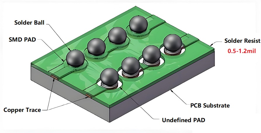
One of the key disadvantages of soldering is the potential for weak joints in high-stress environments. While soldering is sufficient for many electronic applications, it is not ideal for components that need to withstand extreme mechanical stress or high temperatures.
Another disadvantage is the possibility of creating cold joints or bridging between leads, both of which can lead to electrical failure. Cold joints occur when the solder does not completely melt and flow properly, while bridging happens when excess solder connects two or more pins that should remain separated.
What is the most common mistake in soldering?
The most common mistake in soldering is overheating the components. Too much heat can damage sensitive components, including the PCB. It can also cause issues like delamination (separation of layers) and the degradation of solder joints.
Proper heat control and timing are essential to avoid these issues. Another common mistake is insufficient solder or excess solder, both of which can lead to electrical failures.
Conclusion:
In summary, the debate between soldering vs welding ultimately depends on the specific application. Techniques like wave soldering and reflow soldering allow for efficient, high-quality production of PCBs and electronic devices.
At EBest Circuit (Best Technology), we specialize in delivering high-quality PCB solutions with advanced soldering techniques. Reach out to us today for expert advice and solutions. Email: sales@bestpcbs.com