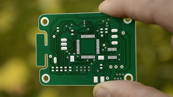
Looking for PCB designing tutorial for beginners? This guide walks through software selection, schematic design, layout optimization, DRC checks, and manufacturing file preparation for first-time PCB creators.
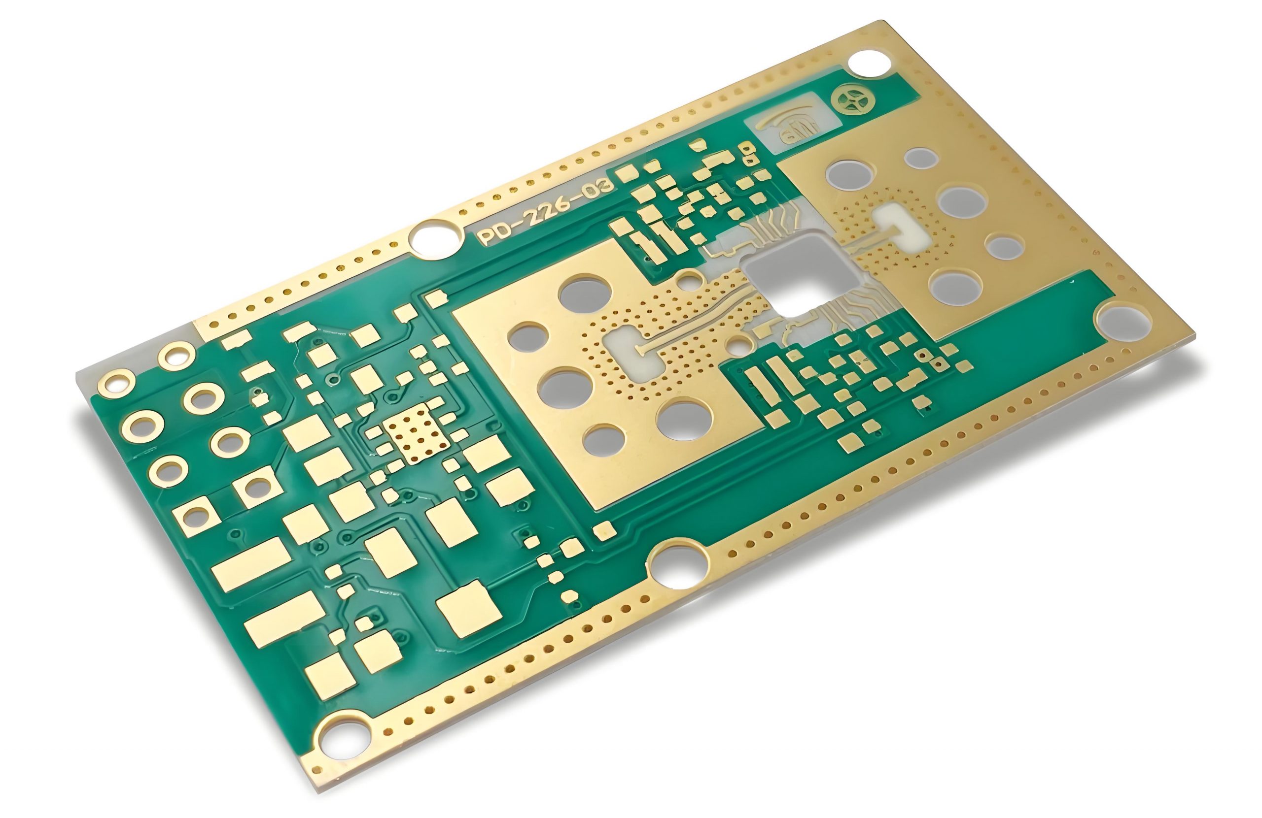
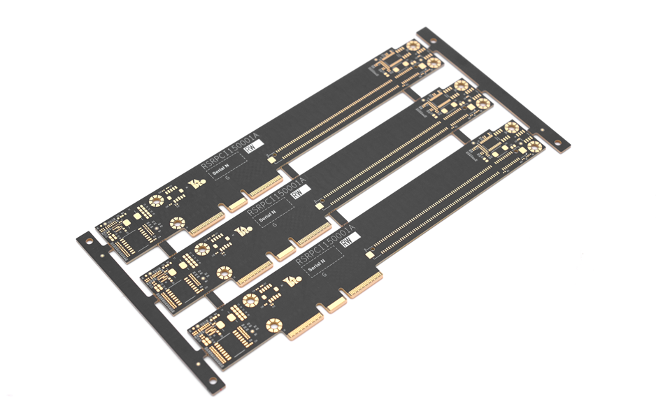
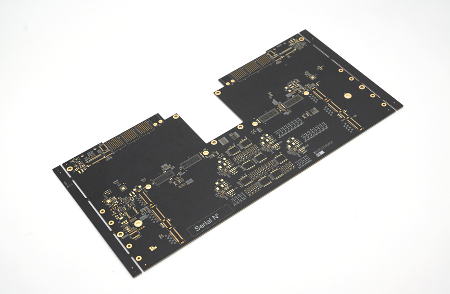
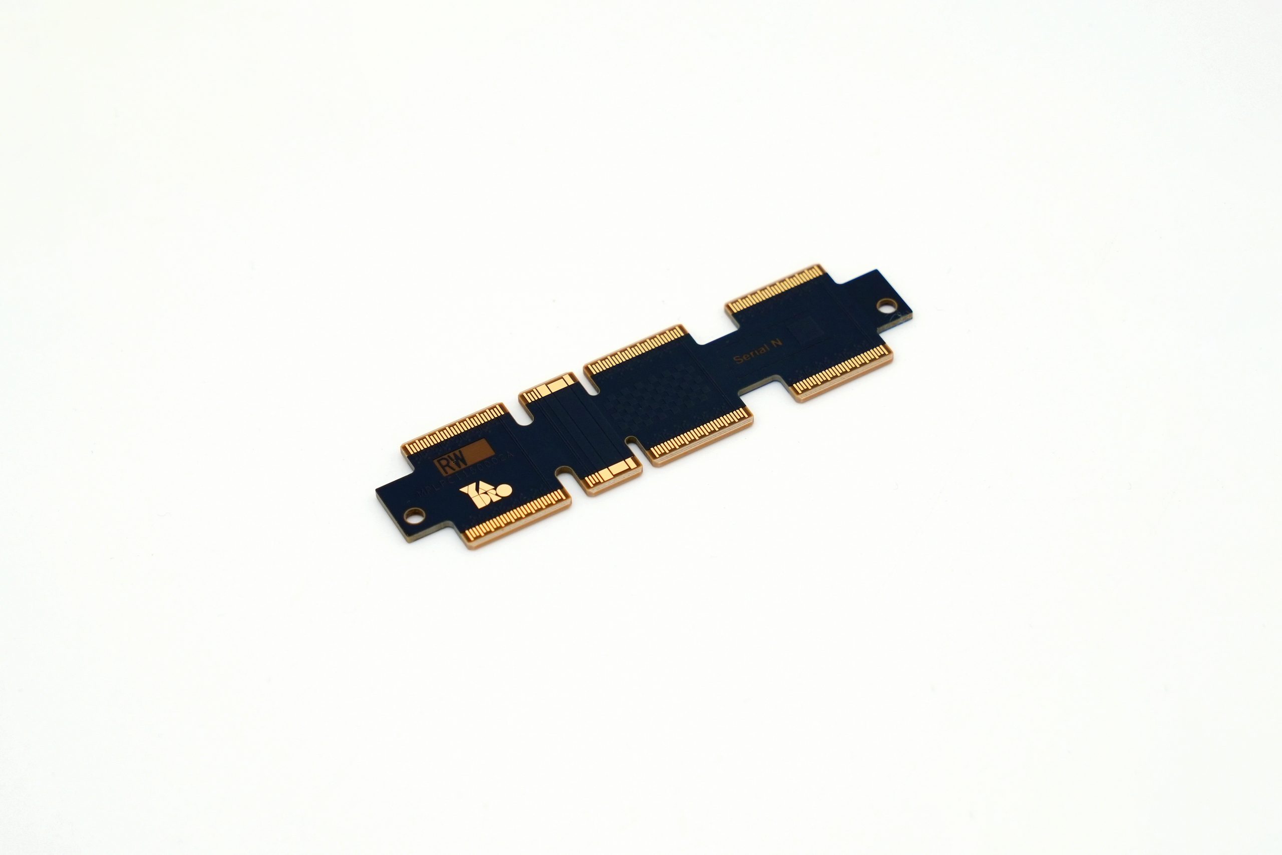
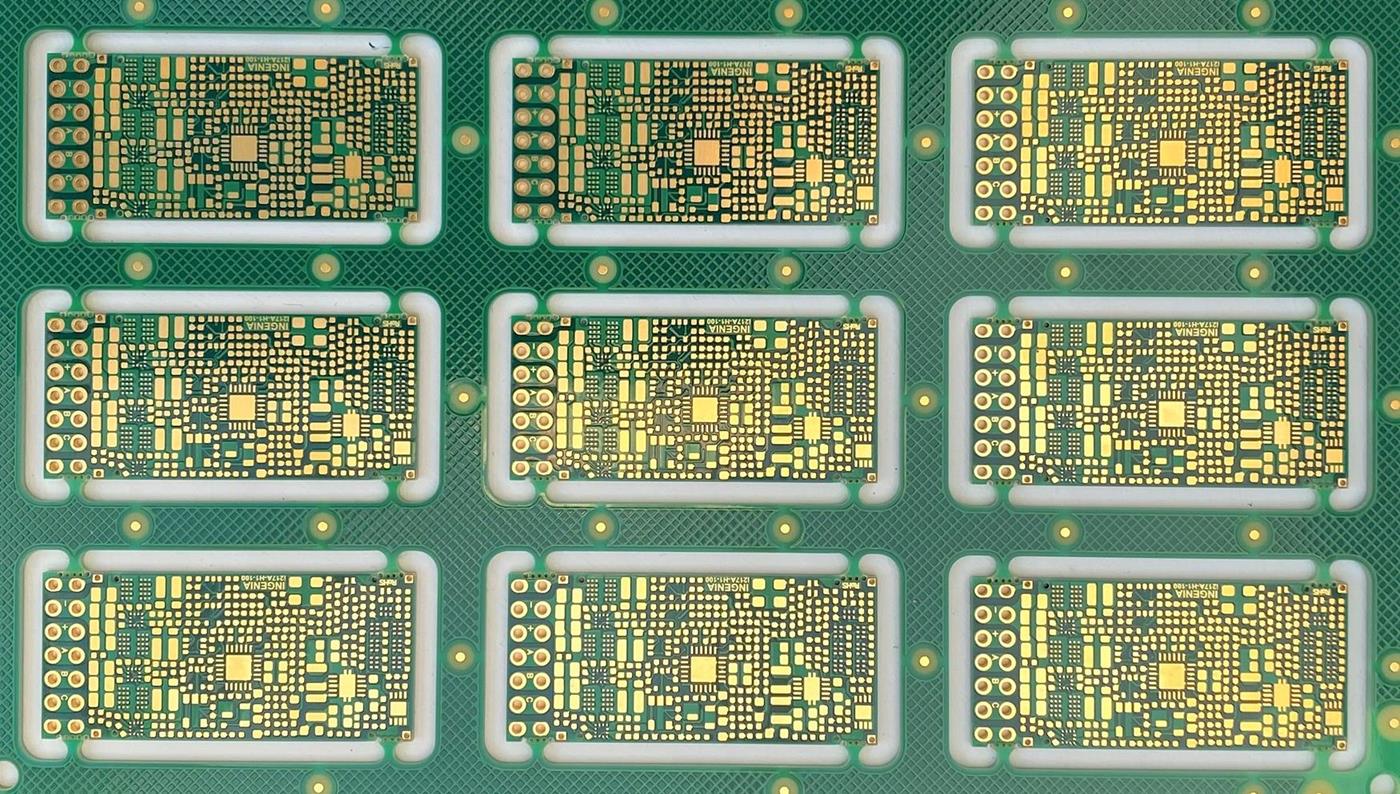
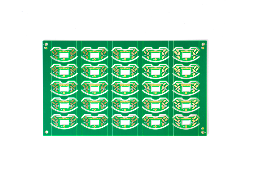
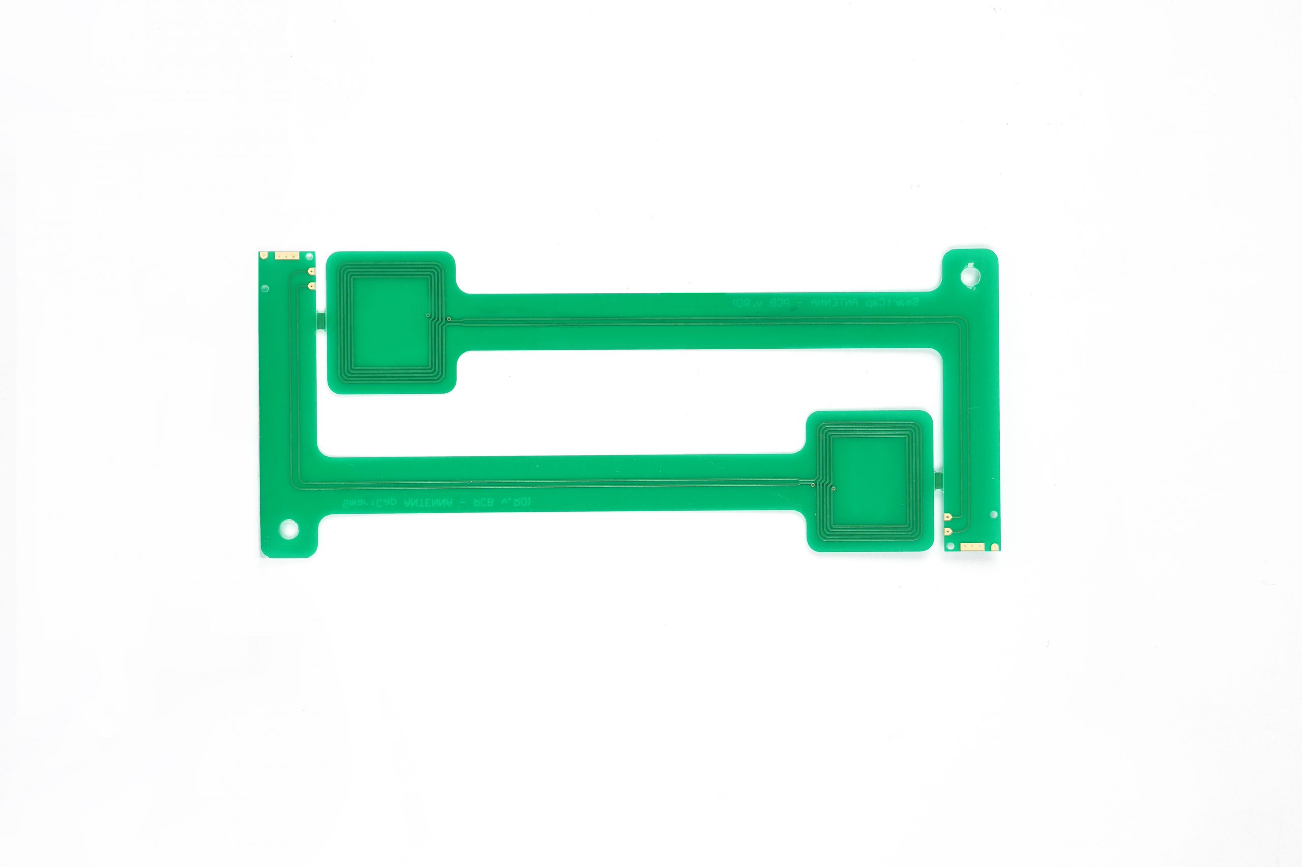
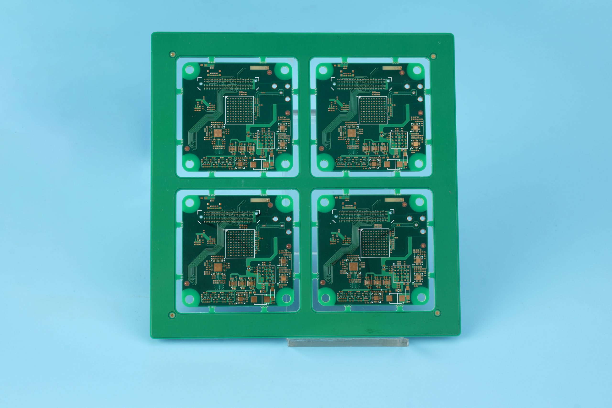
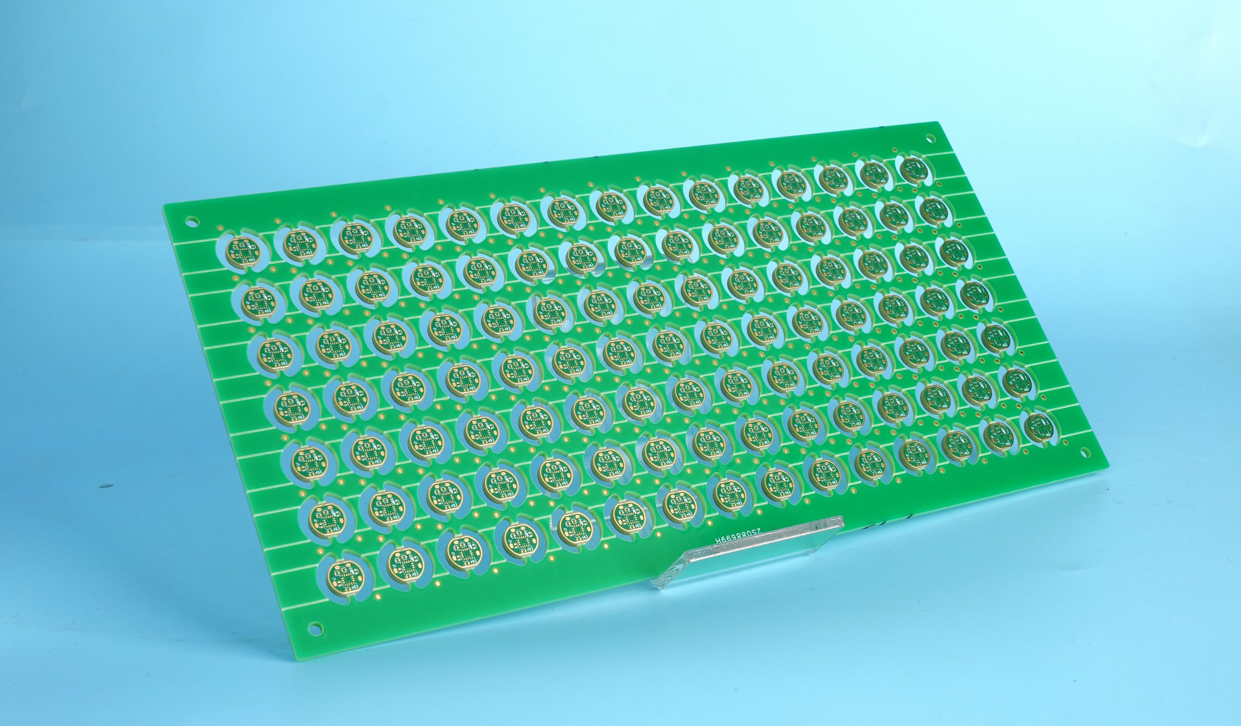
EBest Circuit (Best Technology) empowers your electronics development with a seamless PCB one-stop solution that accelerates time-to-market while reducing risks, including FR4 board, HDI Board design and production. Our engineering-focused approach begins with free DFM analysis to optimize your designs for manufacturability, preventing costly revisions later. A dedicated team of PCB specialists provides real-time multi-engineer support throughout the process, ensuring design integrity from schematic to final product. We understand startups and enterprises alike need flexibility, that’s why we offer prototyping services starting from just 1 piece, with 24-hour rapid turnaround for urgent projects to keep your development cycles agile. Backed by a reliable electronic component supply chain, we eliminate material shortages that commonly delay production. What truly sets us apart is how we integrate manufacturing expertise early in your design phase through collaborative engineering reviews, helping you avoid typical pitfalls in high-speed routing, thermal management, and assembly compatibility. Whether you need quick-turn prototypes or volume production with consistent quality, our streamlined process delivers boards faster without compromising reliability, giving you the competitive edge to launch products when it matters most. Welcome to contact us if you have any request for PCB design or production: sales@bestpcbs.com.
Software & Tools for Beginners in PCB Designing Tutorial
Below are software and tools for beginners in PCB designing tutorial:
1. CircuitMaker (Free, Cloud-Based)
- Best For: Hobbyists and small teams.
- Features: Schematic capture, PCB layout, and autorouting in a unified platform. Integrates with component libraries and offers real-time collaboration.
- Pro Tip: Leverage its community forums for troubleshooting component placement and trace routing.
2. KiCad (Open-Source)
- Best For: Multi-layer designs (up to 32 layers).
- Features: 3D visualization, SPICE simulation, and Gerber file inspection. Modular workflows suit simple prototypes to advanced boards.
- Pro Tip: Start with the built-in tutorials to master library management and footprint customization.
3. EAGLE (Free Tier Available)
- Best For: Single/double-sided PCBs.
- Features: Drag-and-drop placement, design rule checks, and Fusion 360 integration for mechanical design.
- Pro Tip: Use the free tier for learning basics; upgrade later for high-layer-count projects.
4. Proteus Design Suite (Educational Focus)
- Best For: Simulation-driven learning.
- Features: Circuit simulation, microcontroller testing, and IoT component libraries.
- Pro Tip: Experiment with sensor and actuator modules before physical prototyping.
5. Upverter (Browser-Based)
- Best For: Remote collaboration.
- Features: Simultaneous editing, BOM generation, and cloud storage.
- Pro Tip: Ideal for group projects or accessing designs across devices.
6. TinyCAD + FreePCB (Lightweight Combo)
- Best For: Minimalist workflows.
- Features: Basic schematic capture and layout tools without 3D distractions.
- Pro Tip: Perfect for mastering netlist management and footprint association.
7. Autodesk Fusion 360 Electronics
- Best For: Mechatronics integration.
- Features: PCB-mechanical CAD sync, thermal simulation, and generative routing.
- Pro Tip: Use for projects requiring enclosure fit checks early in design.
8. DipTrace (Step-by-Step Tutorials)
- Best For: Custom component creation.
- Features: Shape-based autorouting, 3D previews, and pattern editor.
- Pro Tip: Follow its guided tutorials to learn layer stack-up and DRC settings.

PCB Design Considerations for Beginners
PCB design considerations for beginners:
- Component Placement Strategy: Place critical components (microcontrollers, connectors) near the board’s center or edges based on functionality. Group related parts (e.g., resistors near a microcontroller’s GPIO pins) to shorten traces. Leave space around tall components (e.g., electrolytic capacitors) for 3D assembly.
- Signal Integrity Basics: Separate high-speed traces (USB, HDMI) from low-speed analog signals to prevent interference. Keep trace lengths short for sensitive lines like crystal oscillators. Match trace impedance in high-frequency designs by maintaining consistent width.
- Power Distribution Network (PDN) Design: Use a dedicated power plane for complex boards to minimize voltage drops. For simple projects, use wide traces (e.g., 0.5mm for 5V rails) and place decoupling capacitors (0.1µF–10µF) near IC power pins. Avoid daisy-chaining power connections.
- Thermal Management: Identify heat-generating components (voltage regulators, MOSFETs) during schematic design. Keep them away from temperature-sensitive parts. Add thermal vias under large components (e.g., SOIC packages) and use copper pours for high-power designs.
- Clearance and Creepage Rules: Maintain 0.2mm clearance between traces and pads on 2-layer boards (increase to 0.3mm for high-voltage applications). Label polarity, test points, and assembly notes clearly on the silkscreen without overlapping solder masks.
- Via and Trace Optimization: Use vias sparingly to reduce costs. Avoid right-angle bends; opt for 45-degree angles. Follow the 2W rule (trace width = 2 × pad width) for thermal relief in through-hole components.
- Design for Manufacturing (DFM): Generate RS-274X Gerber files to avoid missing solder mask layers. Include board outlines, mechanical dimensions, and keepout zones. Provide a centroid file for assembly and match component orientations to pick-and-place requirements.
- Documentation and Version Control: Track changes to schematics, layouts, and BOMs in a design history file (DHF). Use version control and label prototype revisions (e.g., “v1.2”) on the silkscreen.
- Testing and Debugging Prep: Add test points for critical signals (I2C, power rails) near board edges. Include a programming header footprint (e.g., 6-pin SWD) for future use. Reserve bottom-layer space for rework on multi-layer boards.
- Iterative Learning Approach: Start with single/double-sided boards before advancing to 4+ layer designs. Review layouts manually before running DRC checks. Adjust designs based on manufacturing quotes (e.g., via-in-pad costs).
Schematic Design Guide for Beginners in PCB Designing Tutorial
Schematic design guide for beginners in PCB designing tutorial:
- Start with a Clear Goal: Before opening software, define your circuit’s purpose. Is it for a robotics project, a home automation gadget, or a basic LED display? List inputs (buttons, sensors), outputs (motors, speakers), and core functions (e.g., “Amplify audio signals” or “Control motor speed”). This keeps you focused.
- Gather Component Details: Collect datasheets for every part you’ll use. Pay attention to pin configurations, voltage requirements, and current limits. For example, a microcontroller’s datasheet might specify that unused pins should be grounded—a detail vital for avoiding errors.
- Choose the Right Tool: Select user-friendly schematic software with drag-and-drop libraries. Options like CircuitMaker, KiCad, or EAGLE offer free tiers with essential features. Explore tutorials to learn basic tools like wire routing, component placement, and annotation.
- Sketch a Block Diagram: Draw a rough block diagram on paper or digitally. Break the circuit into sections: power supply, input processing, core logic, and output drivers. This visual guide prevents chaos as you design.
- Place Components Logically: Arrange symbols to follow signal flow. Place power-related parts (batteries, regulators) at the top, sensors in the middle, and outputs (LEDs, motors) at the bottom. Group passive components (resistors, capacitors) near their active counterparts (ICs, transistors).
- Connect Wires with Intention: Use labeled nets (e.g., “VCC,” “GND,” “DATA”) instead of generic wires. Avoid messy connections by routing wires horizontally/vertically and using junction dots for clarity. For example, connect all ground pins to a common “GND” net to reduce clutter.
- Annotate Like a Pro: Add text labels to explain complex connections. Label resistor networks (e.g., “R1-R4: 10kΩ Pull-Up”) and include component values (e.g., “100nF”) near symbols. This documentation saves time during troubleshooting.
- Run Error Checks: Use the software’s electrical rule check (ERC) to spot issues like unconnected pins or duplicate net names. Manually review the schematic for logic errors, such as reversed diode polarities or incorrect capacitor voltages.
- Simulate If Possible: If your tool supports simulation (e.g., SPICE in KiCad), test subcircuits like filters or amplifiers. For example, simulate an RC low-pass filter to confirm it blocks high frequencies as intended.
- Simplify and Iterate: After initial placement, look for ways to reduce component count. Replace discrete resistors with a single array if possible. Save version backups (e.g., “schematic_v1.sch”) to revert if needed.
- Prepare for PCB Layout: Assign footprints to all components before exiting. Generate a netlist to import into your PCB layout tool. Double-check power/ground nets are named correctly to avoid layout issues.
- Learn from Examples: Study open-source schematics for projects like Arduino shields or sensor modules. Notice how experienced designers organize components and label nets. This exposure accelerates your learning curve.
What Are the PCB Design Rules For Beginners?
PCB design rules for beginners:
- Component Placement Rules: Start by placing core components like connectors, regulators, and microcontrollers near the board’s edges or center. Group related parts together such as resistors near an LED or capacitors close to a power pin. Leave space around tall components for 3D assembly clearance.
- Trace Width Guidelines: Use wider traces for power lines (e.g., 0.5mm for 5V rails) to handle higher currents. Signal traces can be thinner (e.g., 0.25mm) but avoid making them too narrow to prevent manufacturing issues. Match trace widths to component pad sizes for consistency.
- Clearance and Spacing: Maintain at least 0.2mm between traces and pads on 2-layer boards. Increase this to 0.3mm for high-voltage designs. Keep silkscreen labels away from solder pads to prevent smudging during assembly.
- Via Usage: Use vias sparingly to reduce costs. Place them strategically for layer transitions but avoid clustering too many in one area. For high-frequency signals, minimize via stubs to prevent signal reflections.
- Power and Ground Planes: For multi-layer boards, dedicate entire layers to power and ground. This reduces noise and improves thermal performance. On 2-layer boards, use wide traces or copper pours for power rails.
- Thermal Relief: Add thermal relief pads to through-hole components to prevent heat buildup during soldering. Use a spoke-like pattern connecting the pad to the copper pour.
- Decoupling Capacitors: Place decoupling capacitors (0.1µF to 10µF) as close as possible to IC power pins. Connect them directly to the power and ground pins with short traces to filter noise effectively.
- Signal Integrity: Route high-speed signals (e.g., USB, HDMI) away from noisy areas like switching regulators. Keep trace lengths short and avoid 90-degree bends. Use differential pairs for sensitive signals like USB data lines.
- Design for Manufacturing (DFM): Generate Gerber files in RS-274X format to include solder mask layers. Add fiducial markers for accurate assembly. Check board outlines and keepout zones for mechanical compatibility.
- Testing and Debugging: Include test points for critical signals (e.g., I2C lines, power rails) near board edges. Add a footprint for a programming header even if unused initially. Reserve space for rework on the bottom layer.
- Documentation: Label all components, test points, and assembly notes on the silkscreen. Include a version number and date on the board. Provide a BOM with manufacturer part numbers for easy sourcing.
- Iterative Design: Start with simple 2-layer boards before tackling complex designs. Review your layout manually before running DRC checks. Learn from manufacturing quotes by adjusting designs to reduce costs.
How to Do PCB Layout and Wiring Techniques to Save Costs?
Here are methods about how to do PCB layout and wiring techniques to save costs:
- Use Fewer Layers: Prioritize for 2-layer boards instead of 4-layer designs whenever possible. Place components on one side and route traces on the other to avoid blind/buried vias. Reserve multi-layer boards for high-frequency or complex circuits only.
- Standardize Component Footprints: Select common footprints like 0805 resistors or SOIC ICs instead of tiny packages (e.g., 0402). Larger parts are cheaper to assemble and easier to solder manually if needed.
- Optimize Component Placement: Group parts by function to shorten trace lengths. Place tall components (e.g., connectors) along one edge to streamline automated assembly. Avoid spreading components across the board unnecessarily.
- Simplify Trace Routing: Use straight traces and 45-degree angles instead of curves. Avoid narrow traces (below 0.2mm) unless required for high-current paths. Wider traces reduce etching time and lower the risk of manufacturing defects.
- Minimize Via Usage: Limit vias to essential layer transitions. Each via adds to drilling costs and may require plating. For multi-layer boards, use through-hole vias instead of microvias if signal speed allows.
- Reuse Common Rails: Share power/ground planes across multiple sections. For example, a single 5V rail can power both digital logic and low-current analog circuits if noise is managed.
- Choose Cost-Effective Materials: Use FR-4 laminate for most projects instead of high-frequency substrates (e.g., Rogers). Avoid gold plating unless required for harsh environments—HASL or ENIG finishes are cheaper and sufficient for most applications.
- Panelize Boards for Production: Design boards in arrays with V-grooves or tabs for efficient manufacturing. Smaller boards can be combined into panels to reduce setup fees.
- Add Test Points Strategically: Include only essential test points for critical signals (e.g., power rails, communication lines). Avoid overcrowding the board with unnecessary pads that increase testing time.
- Run Design Rule Checks Early: Fix clearance and spacing errors before submitting files. Revisions after fabrication quotes can delay projects and incur redesign fees.
How Can Beginners Perform DRC Checks on PCB Designs?
Here’s how beginners can perform Design Rule Checks (DRC) on PCB designs:
1. Learn the Basics of DRC: DRC tools automatically verify your PCB layout against rules like trace width, clearance, and via limits. They flag issues such as shorts, open circuits, or spacing violations that could cause your board to malfunction.
2. Locate DRC in Your Design Software: Most PCB design tools include a DRC feature. For example, in KiCad, you can find it under “Tools” > “Design Rule Check.” Spend time familiarizing yourself with the interface and available settings.
3. Run DRC Checks Frequently: Perform DRC checks early and often during your design process. Start with a quick check after placing major components to catch obvious errors like overlapping traces or missing footprints.
4. Adjust DRC Rules for Your Project: Tailor the rules to your specific design. For instance, set a minimum trace width of 0.2mm for standard 2-layer boards and increase it to 0.3mm for high-voltage applications. Always refer to your PCB manufacturer’s guidelines for recommended settings.
5. Systematically Address DRC Errors
Review the errors highlighted by the DRC tool, such as red markers in KiCad. Prioritize fixing critical issues first:
- Clearance Violations: Adjust trace or component placement to increase spacing.
- Unconnected Pins: Ensure all component pins are properly connected.
- Shorted Nets: Identify and resolve accidental connections between nets.
6. Use Batch Processing for Efficiency
Some tools allow you to filter errors by type. Tackle high-priority issues like power/ground shorts first, then address less critical warnings such as silkscreen overlaps.
7. Inspect Your Design in 3D
After passing DRC, use your software’s 3D viewer to check for physical collisions between components and enclosures. Tall parts like connectors might interfere with housing even if the DRC is clean.
8. Re-run DRC After Making Changes
Always perform a new DRC check after editing your design. A single change, like moving a trace, could inadvertently reduce clearance elsewhere and introduce new violations.
9. Generate and Save DRC Reports
Create a text report summarizing the DRC results. This document is useful for referencing issues and sharing with your PCB manufacturer to ensure compliance with their capabilities.
10. Learn from Recurring Mistakes
Keep track of common errors you encounter, such as forgetting to place decoupling capacitors. Adjust your design workflow, like using a pre-made template for power circuits, to prevent future issues.
11. Enable Real-Time DRC Feedback
Some tools offer real-time DRC, which provides instant feedback as you design. This feature helps catch errors early and reduces the time spent debugging later.
12. Align Rules with Manufacturing Specs
Ensure your DRC settings match the requirements of your PCB manufacturer. For example, some fabricators specify a 0.15mm minimum hole size instead of the default 0.2mm.
How Do Beginners Export Gerber Files Correctly?
Exporting Gerber files correctly ensures your PCB design translates accurately to manufacturing. Here’s a step-by-step guide for beginners:
1. Finalize Your Design: Complete all layout edits, including traces, component placement, and labels. Run a final Design Rule Check (DRC) to catch errors like missing footprints or clearance violations.
2. Configure Layer Settings
Include all necessary layers:
- Copper Layers: Top and bottom layers (and internal layers for multi-layer boards).
- Silkscreen: Top and bottom labels.
- Solder Mask: Top and bottom masks.
- Paste Mask: For SMT assembly (if needed).
- Outline: Board edges and cutouts.
3. Set Units and Precision: Choose millimeters or inches based on your fabricator’s preference. Use 2.5 or 3.3 numerical precision to avoid rounding errors during manufacturing.
4. Generate Gerber in Your Software: In KiCad, use “File” > “Plot” to open the Gerber generator. In EAGLE, use the “CAM Processor” tool. Select all required layers and enable “Extended Attributes” for component data.
5. Name Files Logically: Use clear names like “Top_Layer.gbl” or “Bottom_Soldermask.gts” to avoid confusion. Some tools auto-generate names, but double-check for clarity.
6. Include Drill Files: Export drill data separately. Ensure drill holes match component footprints (e.g., 0.8mm for through-hole resistors). Check for slotted holes or unusual shapes.
7. Verify with a Gerber Viewer
Open files in a free viewer like Gerbv or ViewMate. Confirm:
- All traces and pads are present.
- Silkscreen labels align with components.
- No extra layers or missing data.
8. Check for Mirror Errors: Ensure the bottom layer isn’t mirrored accidentally. Some tools flip the bottom layer by default—disable this if your fabricator expects raw data.
9. Zip Files for Delivery:
Compress all Gerber and drill files into a single ZIP folder. Include a README.txt with:
- Board dimensions.
- Layer stack-up order.
- Special instructions (e.g., “No gold fingers”).
10. Submit to Fabricators: Upload the ZIP to your PCB manufacturer’s portal. Some providers offer free file checks before payment.
11. Review Fabricator Feedback: Address any issues flagged by the manufacturer (e.g., too-small traces). Resubmit revised files promptly.
12. Save Backup Copies: Keep a copy of your Gerbers and project files locally. This helps if reorders or revisions are needed later.
How Can Beginners Verify the Feasibility of PCB Design?
Beginners can verify PCB design feasibility through these steps:
1.Run Design Rule Checks (DRC): Use your software’s DRC tool to catch errors like trace spacing violations or unconnected pins. Fix issues before proceeding.
2.Check Signal Integrity: For high-speed signals (e.g., USB, HDMI), simulate traces to ensure minimal reflections and crosstalk. Keep lengths short and avoid 90-degree bends.
3.Validate Power Distribution: Confirm power rails (e.g., 3.3V, 5V) have adequate width and decoupling capacitors. Use copper pours to reduce resistance and inductance.
4. Assess Thermal Performance: Check for heat-generating components (e.g., regulators, MOSFETs). Add thermal vias or heatsinks if needed.
5. Review Manufacturability: Ensure trace/space meets fabricator limits (e.g., 0.1mm minimum). Avoid tiny pads or slots that increase costs.
6. Build a Prototype: Order a small batch to test assembly and functionality. Check for soldering issues or mechanical misalignment.
7. Use Free Simulation Tools: Try online SPICE simulators for basic circuit tests. For example, verify a filter’s frequency response before fabrication.
8. Document Everything: Create a BOM with manufacturer part numbers. Include assembly notes for soldering or testing steps.
9. Estimate Costs Early: Use fabricator quote tools to compare prices based on layer count, material, and quantity. Adjust design to fit budget.
10. Seek Feedback: Share your design with online communities or mentors. They might spot issues like component obsolescence or EMI risks.
Conclusion
In conclusion, this beginner’s guide has covered essential PCB design fundamentals from software selection to manufacturing file generation. By following these structured steps including schematic creation, layout optimization, design rule validation, and thorough verification, newcomers can develop production-ready boards with confidence. For professional-grade PCB fabrication with competitive pricing and reliable quality control, request a free quotation from EBest Circuit (Best Technology) today. Their engineering team offers expert guidance to transform your designs into high-performance circuit boards while optimizing cost-efficiency. Start your PCB journey with trusted manufacturing partners.