China ceramic PCB manufacturers are becoming the top choice for companies needing high-performance and heat-resistant circuit boards. Their experience, innovation, and advanced equipment help meet various industry needs. Whether you work in aerospace, automotive, LED, or medical devices, reliable ceramic PCBs are vital. But what makes Chinese suppliers stand out? Let’s explore their strengths and the processes behind their work.
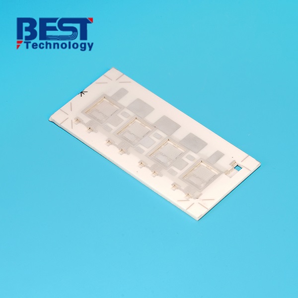
EBest Circuit (Best Technology) is one of the professional China ceramic PCB manufacturers. Our company vision is to be China’s most trusted one-stop ceramic PCB fast solution provider. Our ceramic PCBs include thick film PCB, thin film PCB, DPC PCB, DBC/DCB PCB, AMB PCB, LTCC PCB, and HTCC PCB. EBest Circuit (Best Technology) has continuously optimized the production control process so that we can offer defective-free products to our customers. There is a 97.2% on-time delivery rate in our ceramic PCB manufacturing factory. The monthly capacity in EBest Circuit (Best Technology) is up to 200000 panels. 3067 customers across 40 countries give us good feedback on the quality and the lead time.
If any inquiries about ceramic PCBs, warm welcome to contact us via sales@bestpcbs.com. Once got your approval of ceramic PCB prototypes and the decision of MP (mass production), the fast lead time will be 2-3 weeks.
Ceramic PCB Manufacturing Process
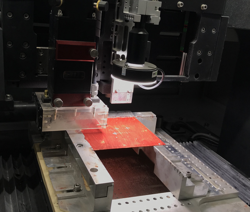
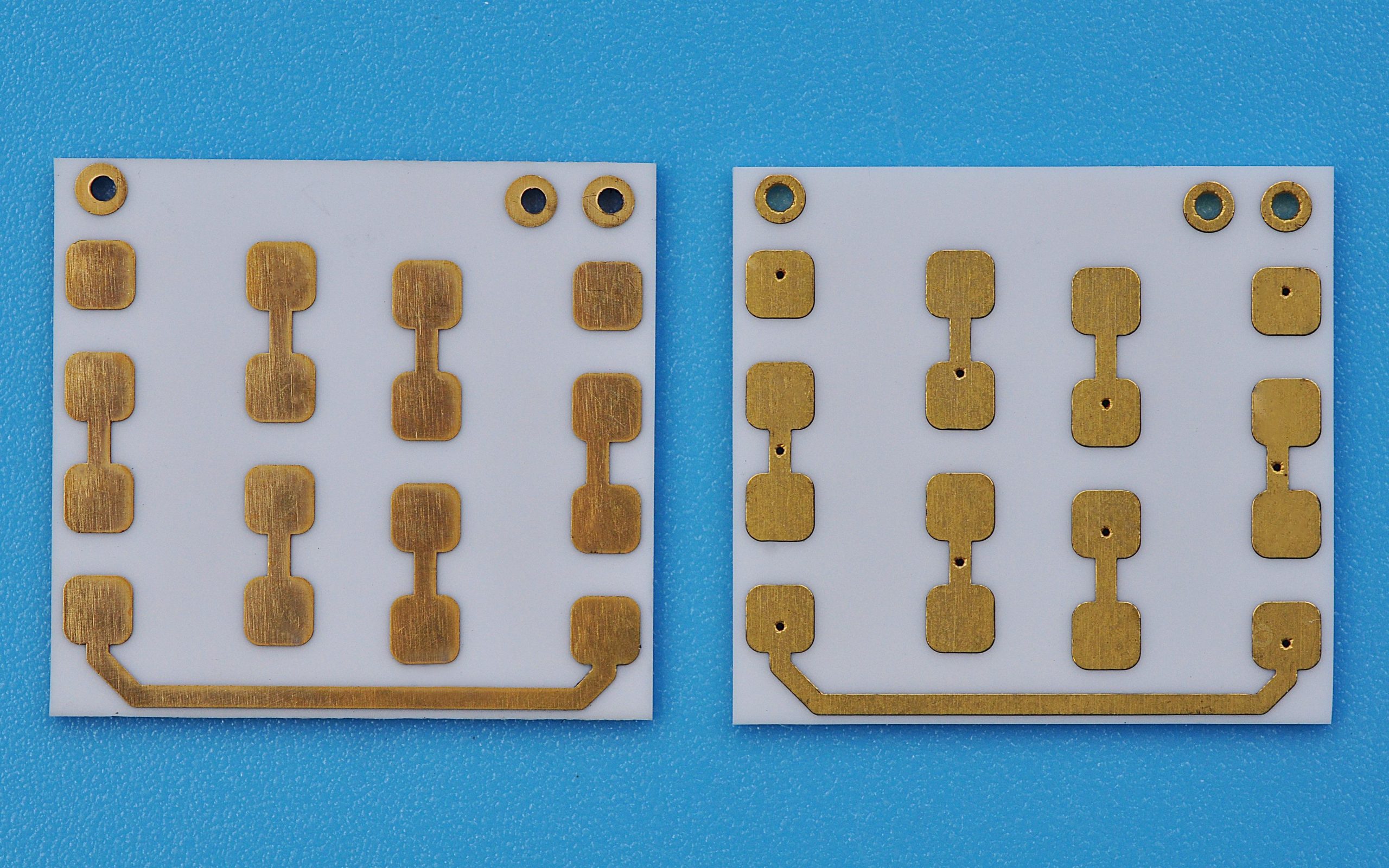
Understanding the ceramic PCB manufacturing process helps you choose the right partner. At EBest Circuit (Best Technology), the DBC (Direct Bonded Copper) production process includes the following steps:
IQC Inspection: Incoming ceramic substrates are carefully checked to ensure they meet specifications.
Laser Drilling: Precise laser machines drill necessary vias and holes.
Vacuum Sputtering (PVD): A thin metal layer is applied to the ceramic surface using Physical Vapor Deposition.
Flash Plating: A light coating is applied for better conductivity.
Pattern Transfer: The design pattern is transferred onto the board using photoresist.
Pattern Plating: Conductive layers are built up in the patterned areas.
Brushing and Polishing: Surface is brushed and polished for smoothness.
Photoresist Removal: Residual photoresist is stripped from the surface.
Etching and Titanium Removal: Unwanted copper is etched off, and any titanium barrier layers are removed.
Electrical Testing: Boards are tested for shorts, opens, and continuity.
Solder Mask: A protective layer is added over areas not meant for soldering.
Pre-Cutting: For silver surface finishes, pre-cutting comes before plating; for gold, it usually happens after.
Surface Treatment: Final surface finish is applied (silver or gold).
Incoming Inspection: Boards are inspected again before moving to final stages.
FQC and FQA: Final Quality Control and Final Quality Assurance ensure boards meet customer standards.
Packing: Boards are cleaned, labeled, and packed for safe delivery.
This well-controlled flow helps reduce defects and maintain high reliability, making Chinese ceramic PCBs a trusted option worldwide.
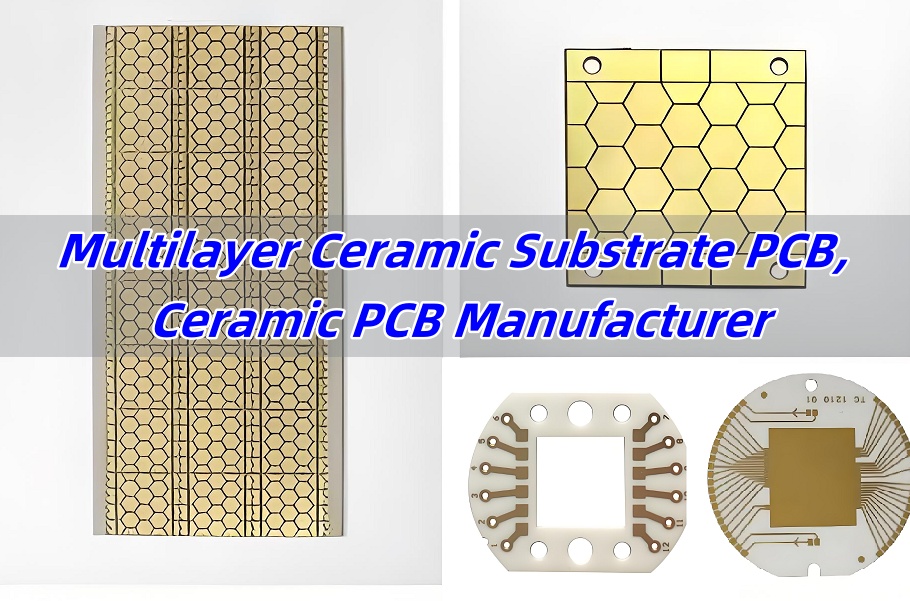
Key Materials Used by China Ceramic PCB Manufacturers in Production
Materials decide how well a ceramic PCB performs. Here are the most used ones:
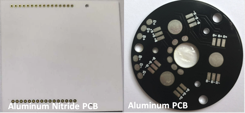
Aluminum Oxide (Al2O3): Common, cost-effective, and offers good insulation.
Aluminum Nitride (AlN): Preferred for its excellent thermal conductivity.
Silicon Nitride: Less common but offers high mechanical strength and resistance to thermal shock.
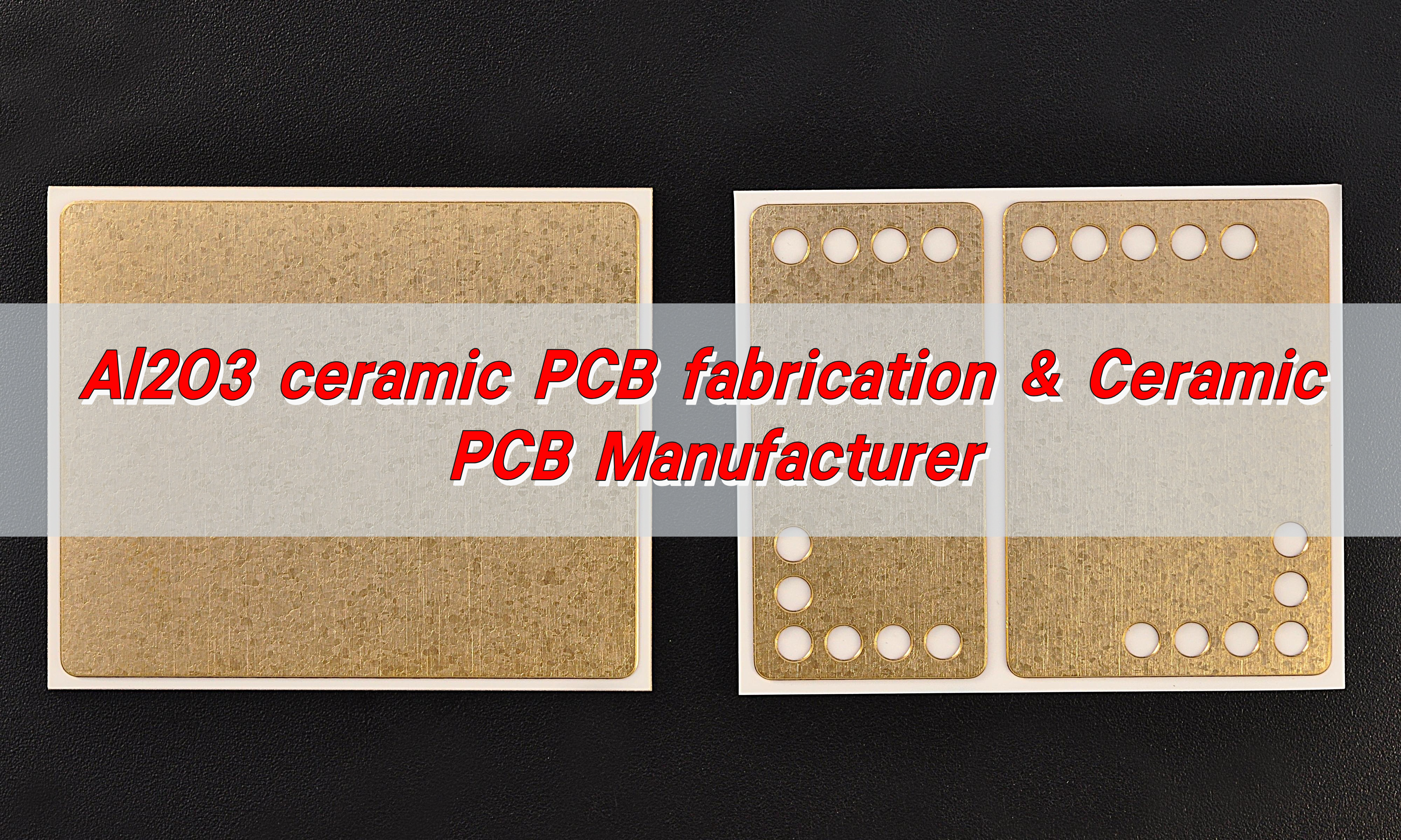
Chinese manufacturers often maintain a stable supply of high-purity materials. This allows consistent performance in each batch. Some even offer custom material blends depending on your needs. As a leading China PCB manufacturer, EBest Circuit (Best Technology) enables full customization across all our ceramic PCB offerings. In reference to EBest Circuit (Best Technology)’s ceramic substrate specifications, the standard thicknesses of Alumina (Al₂O₃) substrates include 0.15/0.25/0.38/0.5/0.635/0.8/1.0/1.2/1.5/2.0 mm. Aluminum Nitride (AlN) substrates are available in 0.15/0.25/0.38/0.5/0.635/0.8/1.0/1.5 mm thicknesses. Non-standard ceramic substrate types require customization. For tailored thickness specifications, kindly consult our account management team or sales engineering specialists to discuss project-specific parameters.
Best China Ceramic PCB Manufacturers
When looking for the best China ceramic PCB manufacturers, consider the following names that regularly top industry reviews:
EBest Circuit (Best Technology): Known for its focus on high-quality ceramic PCBs with fast delivery. BEST offers one-stop EMS ceramic PCB solution without minimum order requirements.
Weller PCB: Offers a wide product range and supports complex, high-mix projects.
Shenzhen Kinwong: One of the largest PCB makers in China with global recognition.
What sets them apart? It’s their constant investment in better machines, tighter process control, and good customer support.
How Do China Ceramic PCB Manufacturers Ensure High Thermal Conductivity?
High thermal conductivity is key for ceramic PCBs. Chinese manufacturers make this happen through several strategies:
Use of AlN substrates: These offer better heat transfer than traditional materials.
Thicker metal layers: Copper or silver layers are optimized for heat spreading.
Advanced firing techniques: This reduces internal voids and boosts thermal flow.
These steps help their ceramic PCBs survive in high-power LED lighting and RF power devices.
What Certifications Do Top China Ceramic PCB Manufacturers Hold?
Certifications add credibility. Most leading China ceramic PCB manufacturers meet strict global standards. Look for these:
ISO 9001: Quality management system
ISO 14001: Environmental responsibility
IATF 16949: Needed for the automotive sector
RoHS & REACH: Compliance for hazardous substances
These certifications show that the manufacturer values safety, sustainability, and precision. EBest Circuit (Best Technology) is certified by the above ISO 9001, and IATF 16949 certifications. All materials are traceable via MES and ERP systems in EBest Circuit (Best Technology). Moreover, the materials we adopt are compliant with UL, RoHS, and REACH. Besides, we are compliant with ISO13485, and AS9100D, which gives us a competitive edge in providing tailored solutions in the medical industry and the aerospace, space, and defense (ASD) industry.
What Sets the Best China Ceramic PCB Manufacturers Apart?
Not all manufacturers are the same. The best ones offer:
Experience: Over 10 years in ceramic PCB manufacturing.
Customization: Ability to make prototypes and high-mix, low-volume orders.
Responsive teams: Fast feedback, technical help, and post-sales support.
Global shipping: Quick delivery to the USA, Europe, and other markets.
Their flexibility helps customers save time and avoid costly delays.
How to Find Reliable China Ceramic PCB Manufacturers for Your Project?
Finding the right partner doesn’t have to be hard. Here’s how to do it smartly:
Research: Start with Google and LinkedIn. Check if they have case studies or client reviews.
Request Samples: Good suppliers will offer test samples.
Factory Audit: If possible, visit or request a video tour.
Communication: A reliable partner will respond quickly and clearly.
Also, choose a supplier who understands your industry. This helps avoid back-and-forth and speeds up your project.
In conclusion, China ceramic PCB manufacturers have evolved into trusted global partners. Their strength lies in combining advanced materials, strong R&D, and top-notch service. They can deliver cost-effective solutions without compromising performance.
If you’re looking for a supplier who values time, quality, and support, it’s smart to consider an experienced name like EBest Circuit (Best Technology). With over 18 years in the PCB industry, we specialize in ceramic PCBs that meet the toughest standards. Reach out to us at sales@bestpcbs.com to get a favorable quote or specification sheet.
With nearly two decades of experience, EBest Circuit (Best Technology) has become one of the most reliable ceramic PCB manufacturers in Asia. We specialize in high-quality ceramic substrate PCBs for a wide range of industries. From automotive to aerospace, from LED lighting to power electronics—we support innovation with strong technical backing and fast delivery.
We don’t just offer boards; we offer tailored solutions. Our team listens carefully, moves quickly, and delivers results. Whether you need AlN, Al₂O₃, or multilayer ceramic PCB, we’ve got your back.
What Is a Ceramic Substrate PCB?
A ceramic substrate PCB is a circuit board made using ceramic materials as the base instead of traditional resins. Unlike FR-4 or other standard materials, ceramics offer excellent heat resistance, thermal conductivity, and mechanical strength.
They’re not just tough—they’re smart. Ceramics can carry high-frequency signals without distortion. They also handle high power loads with ease, which is why they’re often used in power modules and high-speed communication systems.
Ceramic Substrate PCB Types
Ceramic PCBs vary based on two main categories: materials and production techniques.
1. Divided by Materials
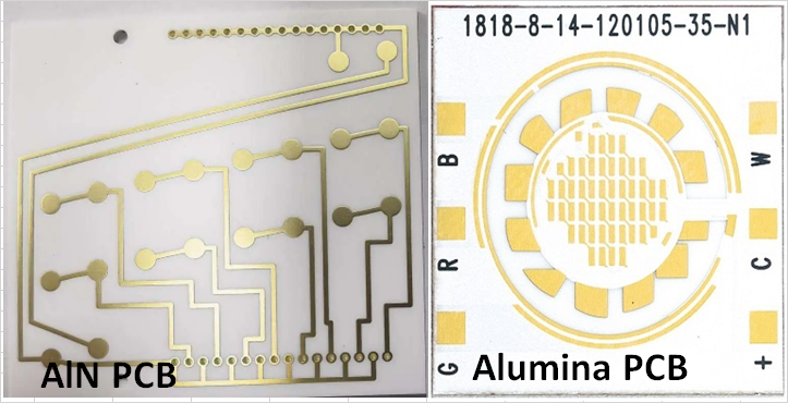
Aluminum Nitride (AlN) PCB
Aluminum nitride PCB is favored for its exceptional thermal performance. Its thermal conductivity ranges from 170 to 230 W/m·K, which is much higher than FR4 or even alumina. It’s often used in power devices, RF modules, and LED lighting. This type also provides strong insulation and good mechanical stability.
Alumina (Al2O3) PCB
Alumina PCBs are the most common type. They offer a balanced mix of electrical insulation, mechanical strength, and cost-effectiveness. They’re available in 96%, 99%, or 99.6% purity levels. The higher the purity, the better the thermal and electrical properties. These boards are widely used in automotive sensors, LED lighting, and industrial controls.
Beryllium Oxide (BeO) PCB
BeO PCBs offer the highest thermal conductivity among ceramic materials—up to 300 W/m·K. However, due to safety concerns during manufacturing, it’s less popular today. Still, for very specific military or aerospace projects, it’s an option. At EBest Circuit (Best Technology), we generally recommend safer materials like AlN or Alumina for most projects.
Silicon Nitride (Si₃N₄) PCB
Silicon nitride offers high strength and fracture toughness. It handles heavy vibration and thermal shock better than others. It performs well in both high-temperature and high-load environments.
Silicon Carbide (SiC) PCB
SiC gaining attention in high-demand environments like electric vehicles and aerospace systems. It offers thermal conductivity in the range of 80 to 180 W/m·K, along with excellent chemical and radiation resistance.
Zirconia (ZrO₂) PCB
Zirconia is known for its toughness and wear resistance. ZrO₂ is used in environments requiring abrasion resistance, such as medical implants, aerospace sealing systems, or sensor housings. It’s not as popular for power electronics but fills special roles where durability matters more than heat dissipation.
2. Divided by Manufacturing Techniques
Thick Film Ceramic Substrate PCB
These use screen-printing to apply conductive and dielectric pastes onto the ceramic surface. It’s reliable, cost-effective, and great for low to medium-volume production. The conductor is usually silver or gold. This type works well for sensors and power hybrid circuits. They also support multilayer designs.
Thin Film Ceramic PCB
This method uses vacuum deposition and photolithography. It’s precise and supports very fine lines and spaces. Thin-film PCBs are more expensive but deliver unmatched performance in miniaturized devices, such as medical implants or RF modules.
DBC Ceramic PCB (Direct Bonded Copper)
DBC PCBs bond copper directly onto a ceramic surface through a high-temperature process. The copper layer is thick and can carry high currents. They are suitable for power semiconductors and automotive applications. They also offer strong adhesion and excellent heat spreading.
DPC Ceramic PCB (Direct Plated Copper)
DPC PCBs are made by plating copper directly onto the ceramic using a chemical process. They can achieve finer features than DBC and are suitable for high-frequency or miniaturized devices.
HTCC involves firing a mix of ceramic and metal powders at over 1600°C. It’s durable and works in harsh environments. HTCC PCBs are commonly used in military and aerospace industries due to their stability under extreme conditions.
LTCC is similar to HTCC but fired at a lower temperature (around 850°C). This process allows for the embedding of passive components, which saves space. It’s perfect for compact, multi-functional devices, especially in telecom and satellite systems. Both HTCC and LTCC ceramic substrate can made into multilayers.
AMB Ceramic PCB (Active Metal Brazing)
AMB PCBs use an active brazing technique to bond copper and ceramic. This method provides better bonding strength than DBC and is ideal for high-load applications like electric vehicles.
Technical Specification of Beryllium Oxide (BeO) Ceramic Substrate
Material Property
Unit
Value
Color
White
Medium grain size
um
3-5
Surface roughness (Ra)
um
0.3-0.5
Density
Kg/m3
3010
Rate of water absorption
%
0
Bending strength
4 point method (40x4x3mm3)
Mpa
400
Dual ring method (0.63mm substrate thickness)
Mpa
500
Thermal conductivity (20-100℃)
W/m-k
220-250
Specific heat
J/kg.K
800
Coefficient of Linear expansion
1*E-6 / K
5.1-8.9
Dielectric constant
6-7
Dielectric loss factor (1 MHz)
1*E-3
0.3
Breakdown Voltage
2.0mm substrate
KV/mm
34
1.0mm substrate
17
0.635mm substrate
11
Volume resistivity
20℃
Ohm * cm
–
Technical Specification of Silicon Nitride (Si₃N₄) Ceramic Substrate
Material Property
Unit
Value
Color
Gray, White, Off-White
Medium grain size
um
3-5
Surface roughness (Ra)
um
0.3-0.5
Density
Kg/m3
3120-3220
Rate of water absorption
%
0
Bending strength
4 point method (40x4x3mm3)
Mpa
147
Dual ring method (0.63mm substrate thickness)
Mpa
490
Thermal conductivity
W/m-k
18.42
Specific heat
J/kg.K
710
Coefficient of Linear expansion (20-1000℃)
10-6/℃
2.8-3.2
Dielectric constant
9.4-9.5
Dielectric loss factor (1 MHz)
1*E-3
0.3
Breakdown Voltage
2.0mm substrate
KV/mm
34
1.0mm substrate
17
0.635mm substrate
11
Volume resistivity
20℃
Ohm * m
1.4*105
500℃
Ohm * m
4*108
Technical Specification of Silicon Carbide (SiC) Ceramic Substrate
Material Property
Unit
Value
Color
Black
Medium grain size
um
3-5
Surface roughness (Ra)
um
0.3-0.5
Density
Kg/m3
3220
Rate of water absorption
%
0
Bending strength
4 point method (40x4x3mm3)
Mpa
400
Dual ring method (0.63mm substrate thickness)
Mpa
500
Thermal conductivity
W/m-k
83.6
Specific heat
-106℃
J/kg.K
399.84
107℃
472.27
247℃
1266.93
Coefficient of Linear expansion (20-1000℃)
10-6/℃
6.28-9.63
Dielectric constant
7
Dielectric loss factor (1 MHz)
1*E-3
0.3
Breakdown Voltage
2.0mm substrate
KV/mm
34
1.0mm substrate
17
0.635mm substrate
11
Volume resistivity
20℃
M * cm
102
Technical Specification of Zirconia (ZrO₂) Ceramic Substrate
Material Property
Unit
Value
Color
White
Medium grain size
um
3-5
Surface roughness (Ra)
um
0.3-0.5
Density
Kg/m3
5850
Rate of water absorption
%
0
Bending strength
4 point method (40x4x3mm3)
Mpa
380
Dual ring method (0.63mm substrate thickness)
Mpa
500
Thermal conductivity
W/m-k
2.09
Specific heat
J/kg.K
563.89
Coefficient of Linear expansion (20-1000℃)
10-6/℃
6.5-11.2
Dielectric constant
27
Dielectric loss factor (1 MHz)
1*E-3
0.3
Breakdown Voltage
2.0mm substrate
KV/mm
34
1.0mm substrate
17
0.635mm substrate
11
Volume resistivity
1000℃
Ohm * cm
104
1700℃
Ohm * cm
6-7
For technical specifications of Al2O3 and AlN, please click hereto view the details.
What Is the Difference Between Ceramic Substrate and FR-4?
Property
Ceramic Substrate PCB
FR-4 PCB
Material Composition
Inorganic (e.g., Al₂O₃, AlN, Si₃N₄)
Organic (Epoxy resin + fiberglass)
Thermal Conductivity
High (AlN: 170–230 W/m·K, BeO: up to 300 W/m·K)
Low (~0.3–0.5 W/m·K)
Operating Temperature
Up to 800°C or more
Limited to ~130–150°C
Electrical Insulation
Excellent and stable
Moderate
Dielectric Constant
Low and stable (AlN ~8.5, Al₂O₃ ~9.8)
Higher and less stable (~4.2–4.8)
Moisture Absorption
None (non-porous)
Yes (hygroscopic)
Mechanical Strength
High (brittle but rigid)
Good flexibility and toughness
Thermal Expansion (CTE)
Very low (~5–7 ppm/°C)
Higher (~14–17 ppm/°C)
RF / Microwave Performance
Excellent (low loss, stable dielectric)
Poor to average (higher signal loss)
Price
Higher
Lower
Application
Focus High-power, high-reliability systems (LEDs, lasers, RF)
General-purpose, consumer electronics
Design Flexibility
Less flexible, requires precise processing
Very flexible, supports complex multilayer structures
How Thick Is a Ceramic Substrate?
Ceramic substrate PCBs come in various thicknesses, depending on the material and application. The most commonly used thicknesses range from 0.25 mm to 3.0 mm. However, special requests can push this range even further.
For alumina, the standard thicknesses are 0.25 mm, 0.38 mm, 0.5 mm, 0.635 mm, 1.0 mm, and 1.5 mm. These sizes work well for LED packages and power control boards.
Aluminum nitride substrates are typically used in 0.38 mm to 1.0 mm thicknesses. The thinner sheets are used in RF circuits, while thicker ones help in thermal management and mechanical support.
Silicon nitride and silicon carbide can also be customized in terms of thickness. Some high-strength applications require boards thicker than 2 mm to add mechanical stability.
For LTCC and HTCC processes, the thickness can vary as layers are stacked. After sintering, the final board may be thinner than expected due to shrinkage. Designers often specify individual layer thicknesses from 100 µm to 300 µm before lamination.
Factors Affect Ceramic Substrate PCB Price
A ceramic substrate price can be varied depends on the material and process used. Here is a detailed explanation.
1. Material Type
Alumina is the most cost-effective, followed by aluminum nitride. Silicon nitride, silicon carbide, and beryllium oxide are more expensive due to material costs and production challenges.
2. Board Size and Thickness
Larger boards cost more to produce. Thicker substrates also require more raw material and longer sintering times, increasing the cost.
3. Layer Count
Single-layer ceramic PCBs are cheaper. Multilayer designs need more lamination and alignment, raising both time and processing costs.
4. Metallization Method
The choice between thick film, DPC, DBC, or HTCC has a big impact. DPC and DBC processes require specialized equipment, so they are more expensive than thick film types.
5. Tolerances and Precision
If your application requires tight tolerances or fine trace widths, this will increase the cost. More precise laser cutting, printing, or etching takes longer and demands higher quality control.
6. Volume
Like most products, higher quantities reduce the per-unit cost. Low-volume or prototype runs are usually priced higher due to tooling and setup.
7. Surface Finish and Testing
Optional services such as ENIG, silver plating, or 100% electrical testing will raise the overall price.
In summary, the price of a ceramic substrate PCB depends on the complexity, material, and quality requirements. While they cost more than FR-4 boards, their performance and longevity often justify the higher investment.
What Is a Ceramic PCB Used For?
High-brightness and long-lifetime lighting
Inverters
IGBTs
Motor drives
Imaging systems
Implants
Diagnostics
Telecom
Antennas
Filters
Base stations
EV batteries
Sensors
Control units
Aerospace
Radar systems
Satellite modules
Multilayer Ceramic PCB Manufacturing Process
Multilayer ceramic PCBs are built using different methods than traditional FR-4 boards. The most popular technique is the thick film, HTCC or LTCC process, which allows stacking multiple ceramic layers with embedded circuits. Here’s a step-by-step look at how they’re made:
1. Ceramic Tape Casting
First, thin ceramic tapes (called green sheets) are cast using alumina, aluminum nitride, or other ceramic powders mixed with binders and solvents. These tapes are then dried and punched to create holes for vias.
2. Via Filling and Screen Printing
Vias are filled with conductive pastes such as gold, silver, or tungsten. Then, a conductive pattern is printed on each layer using screen printing or sputtering techniques.
3. Layer Alignment and Lamination
Multiple layers are stacked together carefully, with precise alignment. They are then laminated under pressure and heat, forming a compact structure ready for sintering.
4. Sintering or Firing
In this step, the laminated structure is fired in a high-temperature furnace—up to 1,600°C for HTCC or 850°C for LTCC. This burns off the organic materials and solidifies the ceramic and metal layers.
5. Metallization and Plating
After sintering, the external layers are coated with surface finishes like silver, gold, ENIG, or nickel. These finishes improve solderability and prevent oxidation.
6. Laser Cutting and Drilling
Final shaping is done using CO₂ or UV lasers. This step defines the board outline and makes precise holes for connectors or mounting.
7. Inspection and Testing
Each board undergoes dimensional inspection, electrical testing, and sometimes X-ray analysis to check for internal defects or misalignments.
Why Choose EBest Circuit (Best Technology) as Your Ceramic PCB Manufacturer?
Let us help bring your next high-performance product to life. Whether it’s Aluminum Nitride PCB, Alumina, or multilayer ceramic PCB, we’re ready to deliver results you can count on.
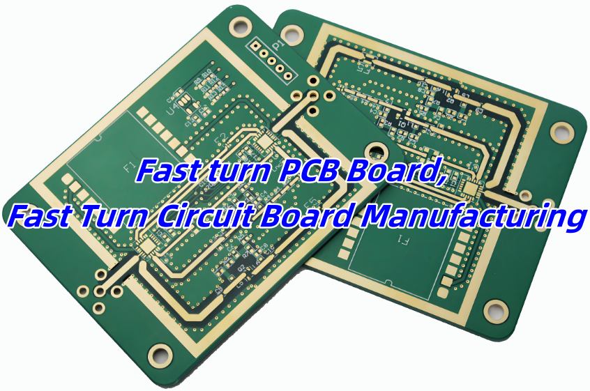
A fast turn PCB board is a printed circuit board manufactured and delivered in a short time, typically within 24 to 72 hours. These quick deliveries help speed up product development, especially during prototyping and pre-production stages. It’s a solution many engineers rely on when time is tight.
Engineers use fast turn PCBs for product validation. They want to see if a new circuit design performs well before moving to mass production. So, getting a board in days instead of weeks can make a huge difference.
First, it speeds up your product timeline. You don’t need to wait weeks to test your circuit. If changes are needed, you can get a revised board quickly and keep things moving forward.
Second, it helps reduce project risks. The faster you test, the faster you detect potential design errors. Early detection saves money and prevents delays.
Third, it improves decision-making. With working samples in hand, your team can test real performance. It’s better than guessing or using simulation data only.
Lastly, fast turn options give your company a competitive edge. Getting to market faster often means better sales and stronger customer trust.
EBest Circuit (Best Technology)’s Typical Turnaround Time for Fast Turn PCBs
At EBest Circuit (Best Technology), we understand the value of time. That’s why we’ve optimized our process to support urgent PCB orders.
For standard 2-layer fast turn PCBs, we usually deliver in 24 to 48 hours. For 4-layer boards, it may take 48 to 72 hours depending on complexity. Our team works around the clock to meet those deadlines.
Even for more complex boards — such as HDI or metal-core PCBs — we still maintain one of the quickest turnaround times in the industry. And we don’t compromise on quality. Each board goes through full inspection and electrical testing before it reaches you. The detailed turnaround time is:
Prototype(<1m²)
Layers
Normal Service
Expedited Service
FR4 PCB
1 Layer
3-4 days
24 hours
2 Layers
4-6 days
24 hours
4 Layers
8-10 days
48 hours
6 Layers
8-10 days
72 hours
8 Layers
10~14 days
72-96 hours
10 Layers
14-18 days
72-96 hours
HDI (1+N+1 2+N+2)
2.5 – 3.5weeks
TBD (depend on design)
We don’t just print boards fast. We manage the process with strict planning, from materials to delivery. That’s why so many clients come back to us for every new project.
Factors That Affect the Turnaround Time of Prototypes
Even though we push for speed, several factors can influence how long a fast turn circuit board takes to produce. Knowing these helps avoid delays.
Circuit Board Design and Test Procedures
The design stage impacts everything. A simple, well-structured layout speeds up processing. Complex routing, fine-pitch components, or tight spacing can add extra review time.
Test procedures matter too. If a special test is needed, like impedance control or functional test setup, it adds to the schedule. Providing clear instructions in advance helps us prepare and avoid delays.
Lamination Cycles
For multilayer boards, each lamination cycle takes time. A 4-layer multi-layer board needs one cycle, while an 8-layer may need several. More layers mean longer pressing times and more careful control.
Quick builds still go through these steps. We just start immediately and plan shifts to manage it faster. That’s why sharing the full stack-up early is so important.
Via-in-Pad Plated Over
Via-in-pad designs are helpful for high-density layouts. But they add a few extra steps in production. We need to drill, plate, and fill those vias carefully. After that, we cap and flatten them before plating the surface.
This extra effort adds time compared to standard vias. If your board uses VIPPO, it’s best to let us know upfront so we can fast-track these processes.
Fabrication Drawing Specifications
Precise drawings help avoid back-and-forth communication. If drawings are unclear or missing details like dimensions, tolerances, or hole types, we’ll need to clarify before production.
Clear drawings lead to fast fabrication. They also reduce the risk of mistakes. That’s why we suggest using IPC-2581 or Gerber X2 format with notes included.
Surface Finish
Surface finish choice also plays a role. ENIG, OSP, HASL, or hard gold all have different process times. For example, ENIG takes longer than HASL because it involves two plating steps.
If speed matters most, we can recommend the best finish based on your needs. Some finishes can still meet performance goals while shaving off hours from the process.
Assembly Drawings and Notes
If you also need PCB assembly, complete documentation is key. Missing part placements, unclear polarity marks, or unreferenced BOM items slow everything down.
Providing all files in one go—BOM, pick and place, centroid file, and notes—helps avoid delays. When everything’s ready, our SMT line can move fast and precise.
Fast Turn Circuit Board Manufacturing
Manufacturing a fast turn circuit board isn’t about rushing. It’s about knowing how to work smart, reduce waste, and prevent rework.
At EBest Circuit (Best Technology), we keep a reserve stock of core materials and prepreg. That way, we can start production immediately without waiting for supply.
We also use automatic routing, inline AOI, and robotic drilling machines to keep operations smooth. Our teams work in shifts, so production doesn’t stop, even at night or on holidays.
Every department is synchronized. CAM engineers review your files fast, material control prepares the stack-up, and QA teams check every step. That’s how we manage fast output without losing accuracy.
We also run a parallel system for urgent jobs. These special jobs go into our “fast-lane” line, separated from standard orders. This ensures time-sensitive boards don’t get stuck behind large-volume orders.
Why Should You Choose EBest Circuit (Best Technology) as Your Preferred Partner?
Experienced team: We’ve been in this field for over 18 years. Our engineers know what works and how to prevent problems early.
Clear communication: Our team responds quickly. We give you updates, clarify questions, and solve problems before they become delays.
Flexible production: Whether you need 1 board or 10,000, we scale easily. We also support special needs like rigid-flex, metal core, or ceramic boards with fast turn options.
Global shipping: We work with trusted logistics partners. Boards reach you safely and on time, even across borders.
Reliable quality: Every board goes through full inspection, AOI, flying probe, and E-test. Even fast jobs go through our strict quality checks.
When you work with EBest Circuit (Best Technology), you get speed, support, and security in every step. That’s why companies in medical, industrial, and automotive industries continue to rely on us.
EBest Circuit (Best Technology) is your trusted partner for comprehensive PCB solutions — from initial concept to final product. With over 18 years of experience, we offer one-stop services that cover the full PCB lifecycle, ensuring high quality, fast turnaround, and competitive pricing. Why customers prefer us:
Free DFM/DFA check
Free Design Guideline
25,000m2 production capacity
2 Hours quick response
Quote within 12 hours
Online support 24/7
Transparent order tracking from first day to final delivery
Military-grade quality boards with strict testing and IPC standards
One-stop services from layout to turnkey assembly
Engineering support to optimize your design for performance and cost
Whether you’re a startup building your first prototype or a large OEM scaling up production, EBest Circuit (Best Technology) is your reliable PCB partner.
Our Core Services – From Design to Assembly
We provide a wide range of services to support your project at every stage:
PCB Design & DFM Check – We don’t just manufacture—we help you build better boards. Send us your layout or concept, and our senior engineers will review your files for manufacturability, improving your design before it hits the production line.
PCB Fabrication – Single-layer, multi-layer, HDI, aluminum-based, or ceramic—we fabricate PCBs of all complexities. Our in-house plant supports quick turnarounds and strict quality control for every batch.
PCB Prototype – Need your prototype in 24–72 hours? We’ve got your back. Ideal for engineers in the development phase, we offer fast PCB prototyping with full traceability, fly-probe testing, and surface finish options.
PCB Assembly – Our turnkey PCB assembly service covers everything from component sourcing, SMT/DIP soldering, to functional testing. You send us your BOM and Gerber—we handle the rest.
IC Programming – Pre-programming and testing of integrated circuits to streamline your assembly process.
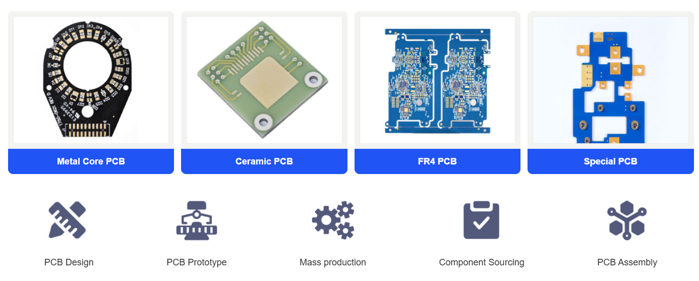
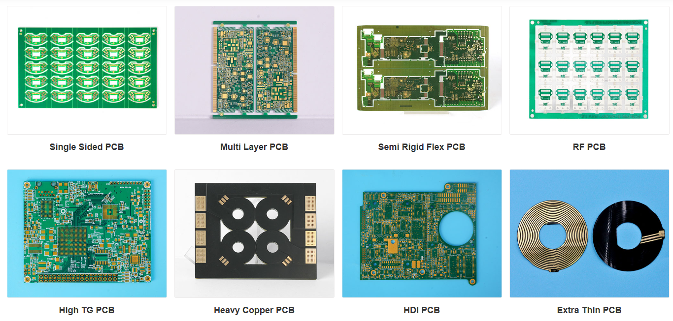
What PCB Types Does EBest Circuit (Best Technology) Manufactured?
We are capable of manufacturing a wide variety of PCB types, including but not limited to:
FR4 PCBs (high speed PCB, IC substrate, high TG PCB, extra thin PCB, our special semi-rigid flex PCB and so on.)
Metal Core MCPCBs (aluminum based PCB, copper clad PCB, sinkpad PCB, thermoelectric copper separate PCB)
Ceramic PCBs (AlN, BeO, Al₂O₃, Zro2)
Flexible and Rigid-Flex PCBs, FFC, Dual access PCB
HDI PCBs
High-Frequency PCBs
Heavy Copper PCBs
Busbar PCBs
Hybrid Substrate PCBs
Whether you need high-reliability boards for aerospace, thermally conductive boards for LEDs, or RF boards for communication devices, we have the capability to deliver.
PCB Prototype Lead Time
We understand how crucial speed is in product development. Our standard PCB prototypelead time is:
Single-layer & double-layer PCBs: as fast as 24 hours
4-layer PCBs: typically 48–72 hours
6-layer or above: around 3–5 working days, depending on complexity
Below is a detailed prototype lead time sheet at EBest Circuit (Best Technology), the expedited options are available to meet urgent project deadlines.
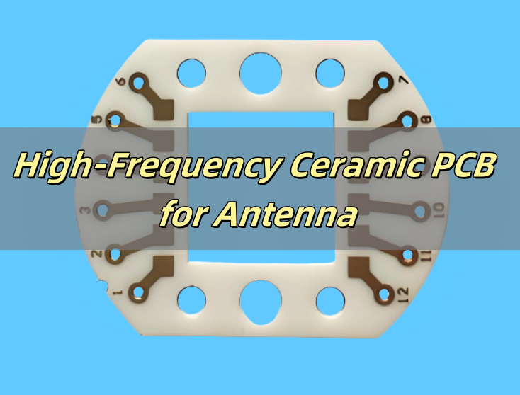
Wireless communication plays a vital role in modern technology. From smartphones to IoT devices, efficient signal transmission is necessary for seamless connectivity. Among the many antenna options, ceramic chip antennas and PCB antennas stand out. Both are widely used in different applications, but they have unique properties that affect their performance.
EBest Circuit (Best Technology) offers ceramic chip antenna design and ceramic antenna manufacturing service over 10 years, we have strong R&D team can assist the design phase, and optimize your ceramic antenna design.
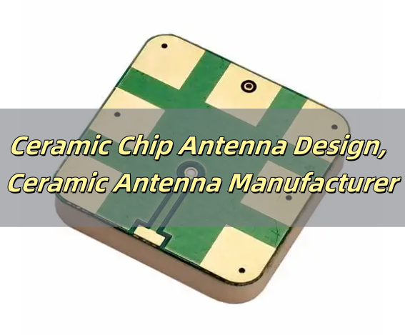
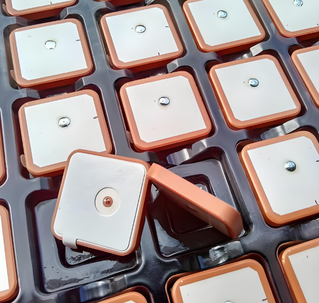
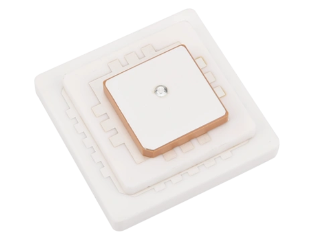
What is a Ceramic Chip Antenna?
A ceramic chip antenna is a compact antenna made from ceramic materials that efficiently transmit and receive radio frequency (RF) signals. Unlike traditional antennas, these are small, robust, and ideal for space-constrained devices.
These antennas operate based on dielectric resonance, where the ceramic material enhances signal propagation. They are commonly used in wireless devices like GPS modules, IoT sensors, Bluetooth-enabled products, and Wi-Fi systems. Due to their small size and strong performance, they are a popular choice in modern electronics.
Features of Ceramic Chip Antennas
Ceramic chip antennas are widely used in wireless communication because of their small size, stable performance, and durability. Unlike traditional metal antennas, they integrate seamlessly into compact devices without sacrificing efficiency. So, what makes them special?
1. Reliable Performance in Any Environment
One of the biggest advantages of ceramic chip antennas is their frequency stability. They can work consistently across different conditions while won’t affect its performance, that’s why they always appear in applications that require high-precision communication, like GPS and industrial IoT devices.
2. Easy to Integrate into PCBs
Ceramic antennas can be directly placed on a circuit board without affecting the overall design. So, engineers can easier to develop sleek and compact electronic devices while keeping manufacturing simple.
3. Small Size and Lightweight
Ceramic chip antennas take up very little space and weigh much less than traditional metal antennas. That’s why they are commonly used in Bluetooth devices, smart wearables, and IoT sensors, where every millimeter matters.
4. Withstands High Temperatures
Some ceramic chip antennas are designed to handle extreme temperatures, even up to 200-300°C.
5. Built for Tough Conditions
These antennas are built to last. They are resistant to interference, lightning, water, and dust, that can withstand outdoor, underwater, and extreme weather applications. From deep-sea exploration to volcanic monitoring, they perform reliably.
6. Strong Signal with Low Power Usage
Even though they are small, ceramic chip antennas provide efficient signal transmission with minimal energy loss. They can help to maintain strong wireless connectivity while reducing power consumption, which is especially useful in battery-powered devices.
Ceramic Chip Antenna Types
Ceramic chip antennas come in different types based on their frequency range, application, and design. Each type serves a specific purpose, whether for Wi-Fi, Bluetooth, GPS, or IoT applications. Below are some of the most common ceramic chip antennas used today.
1. PCB Trace Antenna
A PCB trace antenna is a type of ceramic antenna that is directly etched onto the circuit board using copper traces. It is one of the most cost-effective options but has certain limitations in terms of signal efficiency.
Since these antennas rely on PCB layout design, factors like board thickness, dielectric constant, and trace width impact performance. They are often used in low-cost wireless modules but require careful tuning to function correctly.
2. 2.4GHz Ceramic Chip Antenna
This antenna operates at 2.4GHz, the standard frequency for Wi-Fi, Bluetooth, and Zigbee communications. It offers better performance compared to PCB antennas due to its optimized ceramic structure.
3. ESP32 Ceramic Chip Antenna
The ESP32 is a widely used microcontroller with built-in Wi-Fi and Bluetooth capabilities. Many ESP32-based devices use ceramic chip antennas to enhance wireless communication without increasing size. They can work well with the ESP32 Wi-Fi + Bluetooth module, ensuring stable connectivity in embedded systems. But it has a limitation that its performance can be influenced by nearby metal components, requiring careful PCB layout.
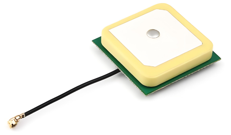
4. GPS Ceramic Chip Antenna
A GPS ceramic antenna is designed to receive satellite signals for positioning and navigation. It is commonly used in devices that require accurate location tracking.
5. Multiband Ceramic Chip Antenna
This antenna is designed to support multiple frequency bands, allowing a single device to operate across different wireless communication standards. They are versatile but limited in expensive manufacturing cost compared to single-band antennas.
So, in a word, if you need a cost-effective and space-saving solution, a PCB trace antenna works well. For Wi-Fi and Bluetooth, a 2.4GHz ceramic chip antenna is ideal. If your project involves IoT and ESP32 modules, go with an ESP32 ceramic chip antenna. For navigation and tracking, a GPS ceramic antenna is the right choice. If you need multiple functions, a multiband ceramic chip antenna offers the most flexibility. The best ceramic chip antenna depends on your end-application.
Ceramic Antenna vs PCB Antenna
PCB antenna is most used in the market, both types have their own strengths and limitations. When selecting an antenna for your application, which is the best? Herein, EBest Circuit (Best Technology) will breakdown their differences in detail:
1. Material and Construction
A ceramic antenna is made from high-quality dielectric ceramic material, it is usually a standalone component that can be soldered onto a PCB. In contrast, a PCB antenna is simply a copper trace printed on the PCB itself, using the board’s material as the dielectric. PCB antennas require precise layout design to function effectively and are directly integrated into the board’s circuitry.
2. Size and Space Efficiency
Ceramic antennas are compact and self-contained, since they do not rely on a large ground plane, they can be placed in confined areas without significant loss in performance. PCB antennas, however, require a larger surface area to achieve good performance, as their efficiency is heavily dependent on ground plane size. In very small devices, a PCB antenna may not be practical due to space constraints.
3. Manufacturing and Design Flexibility
A PCB antenna is cost-effective and easy to manufacture since it is created directly on the PCB during the etching process. This eliminates the need for additional components, reducing bill of materials (BOM) costs. However, PCB antennas require careful tuning and optimization, so its design and manufacturing process more complex.
4. Cost and Production Considerations
PCB antennas are generally cheaper to produce, as they are just part of the PCB layout and do not require separate assembly. However, the hidden cost comes in the form of design complexity, tuning, and potential performance issues. Ceramic antennas, while having a higher unit price, reduce design time and improve reliability, leading to lower costs in the long run for high-performance applications.
How Does a Ceramic Antenna Work?
The working principle of ceramic antenna PCB mainly includes two processes of transmitting and receiving. The ceramic antenna uses GPS satellite to realize navigation and positioning. The main task of the user’s receiver is to extract the pseudo-random noise code and data code in the satellite signal, so as to solve the navigation information of the receiver carrier such as position, speed and time (PVT). Here is a detailed explanation for each process:
Signal Transmission – The antenna converts electrical signals into electromagnetic waves.
Signal Reception – It captures incoming RF signals and converts them back into electrical signals.
Impedance Matching – A matching network ensures efficient energy transfer between the antenna and the circuit.
Ground Plane Interaction – A well-designed ground plane improves signal stability and efficiency.
Ceramic Chip Antenna Design Considerations
Designing a ceramic chip antenna involves several factors that influence performance. Here are the key considerations:
1. Antenna Placement on the PCB
Antennas should be positioned at the edge or corner of the PCB to maximize radiation efficiency. Nearby metal components, shielding, or large ICs should be avoided as they can cause signal interference.
2. Ground Plane Size and Layout
A larger ground plane improves antenna efficiency by acting as a signal reflector. The PCB material should match the antenna’s specifications to maintain frequency accuracy.
3. Antenna Matching and Impedance Tuning
Most ceramic antennas are designed for 50Ω impedance, but variations in PCB layout can affect this. A matching network, typically using capacitors and inductors, engineers often use Pi or T matching networks to fine-tune performance.
4. Clearance and Keep-Out Zones
There should be no copper traces, ground planes, or metal components too close to the antenna. Keeping the antenna away from batteries, shields, and enclosures.
5. Operating Frequency and Bandwidth Considerations
Each ceramic antenna is designed for a specific frequency, such as 2.4GHz for Wi-Fi/Bluetooth or 1.575GHz for GPS. Any change in PCB layout can shift the resonance frequency, requiring fine-tuning.
What is the Most Effective Ceramic Antenna Shape?
The shape of a ceramic antenna influences its performance. The most effective shapes include:
Rectangular: Common in chip antennas, offering a balance between size and performance.
Helical: Provides better bandwidth and efficiency in small spaces.
Patch: Ideal for GPS applications, offering strong directional signals.
Planar Inverted-F Antenna (PIFA): Compact and efficient, widely used in mobile devices.
With over a decade of effort and experience, EBest Circuit (Best Technology) has been actively contributing to the growth of this business. Certified with ISO9001, ISO13485, IATF16949, AS9100D,UL, and RoHS, the company is fully capable of delivering high-performance, eco-friendly PCBs and various types of ceramic chip antenna for various applications at competitive prices. If choose EBest Circuit (Best Technology), you can enjoy:
Expertise – Decades of experience in antenna design and PCB manufacturing.
Custom Solutions – Tailored ceramic antennas based on customer requirements.
Strict Quality Control – Every product undergoes rigorous testing to ensure top performance.
Competitive Pricing – High-quality antennas at cost-effective prices. DDU & DDP quotation available.
Global Support – Trusted by customers worldwide for reliable wireless solutions.
5 Years Guarantee – Offer free repairing and re-work if products have quality issue within 5 years.
For businesses looking for top-tier ceramic antennas, EBest Circuit (Best Technology) delivers innovative and high-performance solutions. Contact us today to discuss your antenna needs!
2.4 GHz antenna plays a key role in wireless communication today. From WiFi routers to smart home devices, they keep us connected without messy cables. Whether you need reliable coverage for short-range indoor use or long-range outdoor connections, the right 2.4 GHz antenna can improve your system’s performance. EBest Circuit (Best Technology) handle both design and production for 2.4Ghz antenna PCB, we can optimize performance from the start. When you need reliable 2.4 GHz antenna PCB, EBest Circuit (Best Technology) delivers top-quality solutions tailored to your project.
What is a 2.4 GHz Antenna?
A 2.4 GHz antenna is a specialized antenna that operates within the 2.4 GHz frequency band. This frequency is widely used for wireless technologies like WiFi, Bluetooth, and IoT devices.
Because 2.4 GHz antennas work within this popular band, they support many devices and systems. Whether for indoor use or longer outdoor coverage, they can send and receive signals efficiently. Their design focuses on matching frequency requirements while balancing gain, size, and range.
What Are the Different Types of 2.4 GHz Antennas?
There are several 2.4 GHz antenna types designed for different environments and needs. Each type offers distinct features to match specific wireless setups.
1. By Radiation Pattern
Omnidirectional Antennas
Omnidirectional antennas send signals in all directions. Radiate signals in all directions horizontally, like ripples on water. They are ideal for indoor WiFi routers or small IoT devices where full-area coverage matters most. (e.g., Wi-Fi routers, smart speakers).
Directional Antennas
Directional antennas focus energy in one direction to boost signal strength over longer distances. Focus energy like a flashlight beam. These are perfect for point-to-point outdoor links, long-distance links (e.g., outdoor cameras, wireless bridges).
2. By Integration Method
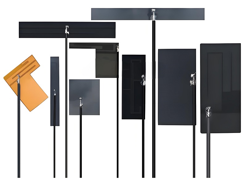
PCB Antennas
PCB Antennas are designed as copper traces embedded directly into circuit boards. Ideal for mass-produced devices due to low cost and space-saving design. Common in Bluetooth earphones, smart thermostats, and IoT sensors. Their performance depends on board material (e.g., FR4 for basic needs, Rogers substrates for high-frequency stability). Requires precise impedance matching to avoid signal loss.
Flexible Antennas
Flexible Antennas are made with thin, bendable materials like polyimide film or flexible printed circuits (FPC). Withstands repeated bending, making them perfect for wearables (e.g., fitness bands) or devices with curved surfaces (e.g., medical patches). Some models survive 100,000+ bend cycles. Water-resistant options available for outdoor gear.
3. By Installation Location
Internal Antennas
Integrated within the device housing, optimized for compact designs and aesthetic concealment. Common in consumer electronics (e.g., smartphones, smartwatches) where space and design are critical. Typically use PCB or flexible antennas for seamless integration
External Antennas
Mounted outside the device via connectors (e.g., SMA) or cables, enabling flexible placement for optimal signal reception. Ideal for environments requiring tunable orientation or signal amplification (e.g., industrial routers, drones). High-gain directional variants (e.g., Yagi-Uda) are often external for long-range applications.
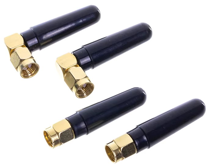
The reason 2.4GHz antennas widely adopt SMA connectors is threefold:
Superior high-frequency performance – low loss (<0.1 dB @ 2.4GHz) and stable 50Ω impedance up to 18GHz;
Robust mechanical design – compact threaded interface ensuring durability in space-constrained devices like drones;
Regulatory compliance – standardized variants (e.g., RP-SMA) meet FCC/CE certifications for Wi-Fi routers and IoT equipment.
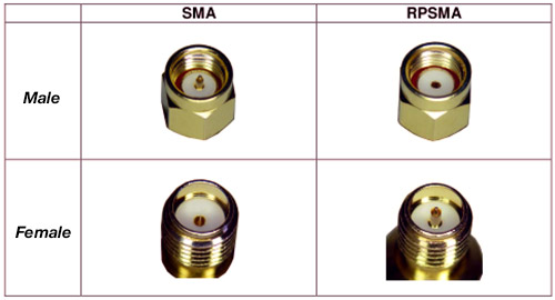
SMA Connector has gender identification. Most antennas use female SMA connectors (hole), while devices (e.g., routers) use male SMA ports (pin). SMA Connector Gender Identification:
SMA Male (Plug): Features a center pin and inner threads.
SMA Female (Jack): Has a center hole and outer threads.
Reverse-polarity SMA (RP-SMA) swaps genders, common in Wi-Fi gear. Pls always check device specs to avoid mismatches.
What Materials Are 2.4 GHz Antennas Made Of?
The materials used to build a 2.4 GHz antenna directly affect how well it performs, how long it lasts, and how easy it is to fit into different devices. Choosing the right materials helps balance conductivity, weight, cost, and durability. Let’s break down the most common material choices and where they fit best.
1. Conductive Metals for High Signal Efficiency
The main goal of any 2.4 GHz antenna is to efficiently radiate and receive signals, so the core material must conduct electricity well.
Copper is one of the top choices. Its excellent conductivity helps signals pass through with minimal loss, which directly improves antenna efficiency. Copper is widely used in both external and internal antennas, particularly in applications where high performance is critical.
Aluminum offers another option, especially for larger antennas where weight savings are important. Although aluminum’s conductivity is lower than copper’s, it’s still good enough for many 2.4 GHz antenna applications, especially directional designs like Yagi antennas or outdoor panels.
These metals form the main radiating elements in most antennas, whether they’re external, internal, or PCB-based.
2. Ceramic for Compact Embedded Designs
When devices shrink, so do their antennas. Many modern devices rely on ceramic antennas, especially for built-in 2.4 GHz antenna PCB layouts.
Ceramic materials allow antennas to stay small without losing too much performance.
They handle higher frequencies like 2.4 GHz well, making them perfect for compact gadgets such as IoT sensors, smart home devices, fitness trackers, and smartphones.
Ceramic antennas are often printed directly onto the PCB or mounted as small components. Their high dielectric constant helps keep the physical size small while still maintaining reasonable performance.
3. Protective Coatings and Weatherproof Materials
For outdoor applications, 2.4 GHz antennas face a different challenge—exposure to sun, rain, and extreme temperatures. Materials used in these antennas need to survive tough conditions without affecting performance.
Many outdoor antennas use weather-resistant plastics to cover the metal radiators. This plastic shielding blocks moisture and dirt but allows radio signals to pass through with minimal interference.
In harsher industrial or marine settings, UV-resistant coatings and corrosion-resistant metals add extra protection, keeping antennas working reliably for years.
These protective materials make sure outdoor antennas can handle long-term exposure while still providing stable connections, even in challenging environments.
2.4 GHz Antenna Design
How to design a 2.4 GHz antenna? Designing a 2.4 GHz antenna may look simple on the surface, but every step directly affects how well the antenna performs. Engineers focus on balancing frequency, size, gain, and impedance matching to get the best signal strength and stable connection. Below is a clear step-by-step breakdown of the key stages.
1. Selecting the Right Antenna Type and Length
The first step in the design process is deciding which 2.4 GHz antenna type works best for the device and its application. Common options include omnidirectional antennas, directional antennas, and PCB-integrated antennas.
Omnidirectional antennas radiate signals evenly in all directions, which suits routers, smart home devices, and wireless cameras.
Directional antennas focus the signal in one direction, which helps with long-range connections or point-to-point communication.
PCB antennas fit directly onto the circuit board, making them perfect for compact gadgets like wearables and IoT devices.
Once the type is clear, the 2.4 GHz antenna length becomes critical. For 2.4 GHz signals, a quarter-wavelength antenna is roughly 31 mm, while half-wavelength antennas are about 62 mm. These values shift slightly depending on the design and placement, especially in small or embedded products. Keeping the length correct ensures the antenna resonates properly at 2.4 GHz, which directly impacts performance.
2. Shaping the Antenna and Optimizing Radiation Pattern
The next important part is choosing the antenna shape since it directly affects how the antenna radiates signals. Different shapes suit different needs:
Helical antennas (coiled wire designs) work well when space is extremely limited. Despite the compact form, they still deliver usable performance.
Patch antennas, often seen in routers and access points, offer reliable coverage with a relatively small footprint.
Monopole or dipole antennas strike a balance between size and performance, making them versatile for indoor and outdoor devices.
Once the shape is selected, engineers use simulation software to model how the antenna radiates at 2.4 GHz. These simulations reveal weak points, dead zones, or unexpected reflections that could weaken signal strength. The design can be adjusted to boost coverage, reduce interference, and fine-tune the antenna’s radiation pattern.
3. Ensuring Proper Impedance Matching and Minimizing Interference
With the physical design in place, attention shifts to impedance matching—a critical factor for signal transfer efficiency. The 2.4 GHz antenna must match the output impedance of the connected device, typically 50 ohms. A mismatch causes signal reflections, which lower efficiency and reduce range.
The antenna materials, trace width, and even the 2.4 GHz antenna PCB layout all affect impedance. Engineers adjust these factors during prototyping to get the cleanest match possible.
Finally, interference checks are essential. The 2.4 GHz band is crowded, with Wi-Fi, Bluetooth, and countless smart devices all sharing the same space. Good antenna designs use filtering techniques, proper shielding, and smart placement to reduce noise from nearby electronics. By minimizing interference, the antenna delivers cleaner signals and better reliability, especially in busy environments like homes and offices.
EBest Circuit (Best Technology) offers a full range of high-quality antenna PCBs, customized to match the unique requirements of each customer. With competitive ODM & OEM pricing, we deliver reliable 2.4 GHz antenna solutions to support your projects from initial design to final production.
What Are the Benefits of 2.4 GHz Antennas?
The 2.4 GHz antenna stands out in the wireless world thanks to its strong performance across various devices and environments. Its advantages explain why it plays such a key role in modern communication systems. Let’s break down some of the key benefits.
1. Compatibility Across Multiple Technologies
One of the biggest benefits of a 2.4 GHz antenna is its broad compatibility. It works smoothly with popular wireless standards like WiFi, Bluetooth, Zigbee, and proprietary RF systems.
This flexibility allows engineers to create devices that communicate across homes, offices, factories, and even outdoor spaces—all using the same frequency band. Because so many devices operate at 2.4 GHz, businesses and designers can standardize around this frequency, reducing complexity when building connected systems.
2. Longer Range Compared to Higher Frequencies
Another key advantage is range. Compared to higher bands like 5 GHz, the 2.4 GHz antenna supports better signal penetration and wider coverage.
Signals at 2.4 GHz travel farther, especially indoors where walls, furniture, and other obstacles can block higher frequencies. This longer range is valuable for applications like smart homes, industrial sensors, and outdoor IoT systems where stable connections matter more than speed.
This is why 2.4 GHz antennas remain so popular, even though faster frequencies exist.
3. Flexible Designs for Every Application
The 2.4 GHz antenna can be designed to match almost any requirement.
For compact devices like wearables or sensors, tiny PCB antennas fit directly onto circuit boards without adding bulk.
For outdoor or long-distance uses, larger high-gain directional antennas focus signals in a specific direction to improve coverage and signal strength.
This range of options—from small embedded antennas to large external ones—gives designers freedom to choose the perfect antenna for each product.
What Are the Applications of 2.4 GHz Antennas?
Because the 2.4 GHz antenna combines wide compatibility, reliable range, and flexible designs, it fits into countless industries and use cases. From home networks to industrial automation, this frequency keeps devices connected in every corner of life.
1. Smart Homes and Consumer Electronics
In residential settings, 2.4 GHz antennas power the everyday devices people rely on.
WiFi routers use 2.4 GHz to provide whole-home coverage, especially in multi-story homes where walls and floors block higher frequencies.
Smart TVs, security cameras, smart plugs, and speakers also connect using this band, ensuring devices stay linked to home networks without constant dropouts.
Even smaller gadgets like smart thermostats, light switches, and door sensors all benefit from the reliability of 2.4 GHz antennas.
2. Industrial and Agricultural Systems
Beyond homes, 2.4 GHz antennas support critical wireless links in factories, warehouses, and farms.
In industrial automation, machines rely on 2.4 GHz wireless connections to report performance data and receive remote commands.
In smart agriculture, wireless soil sensors, irrigation controllers, and livestock trackers all depend on 2.4 GHz antennas to transmit data across fields and greenhouses.
These industries value 2.4 GHz for its range, penetration, and low power requirements, making it ideal for sprawling facilities and remote locations.
3. Automotive and Healthcare Technologies
The automotive and medical sectors also take advantage of 2.4 GHz antennas in innovative ways.
Connected vehicles use them to communicate with roadside sensors, smart traffic lights, or other vehicles nearby.
In healthcare, patient monitors, wearable health trackers, and wireless diagnostic tools rely on 2.4 GHz to continuously transmit data to caregivers without using wired connections.
Because 2.4 GHz antennas balance reliable performance and compact size, they work perfectly in cars and medical devices where space and reliability matter most.
2.4 GHz Antenna PCB Manufacturer
Why choose EBest Circuit (Best Technology) as your trusted 2.4 GHz antenna PCB manufacturer? When choosing a 2.4 GHz antenna PCB manufacturer, you want more than just a product — you need a partner who understands your industry, your project requirements, and your timeline. At EBest Circuit (Best Technology), we deliver all that and more. Here’s why companies worldwide trust us for their 2.4 GHz antenna needs:
1. Full Turn-key Antenna PCB Solutions
At EBest Circuit (Best Technology), we do more than supply antennas PCB — we work alongside you from initial design all the way to final delivery. Whether you need a standard design or something fully customized to match your device size, operating environment, and signal requirements, we’ve got you covered.
2. 18 Years PCB Manufacturing Experience
With over 18 years of hands-on experience in PCB manufacturing, our engineering team ensures your antenna’s performance is fine-tuned from the start. By handling both design and production under one roof, we make sure every detail — from material selection to layout optimization — works in harmony to maximize performance.
3. No MOQ Requirement
We also provide flexible order sizes, whether you need a small prototype batch for testing or high-volume production for mass deployment. With no MOQ restrictions, we ensure rapid turnaround times and dedicated support for projects of any scale.
4. 2-3 Weeks Fast Delivery Time
With delivery times as fast as 2-3 weeks, we help you hit your project milestones without compromising on quality. Our streamlined production process and dedicated team ensure timely delivery to keep your projects on track.
5. High Quality Ensured
Reliability matters, especially for wireless communication. Every PCB of 2.4 GHz antenna from EBest Circuit (Best Technology) undergoes thorough performance checks to ensure it meets frequency accuracy, gain, and long-term durability requirements.
6. ISO13485, IATF16949 & AS9100D Compliant
Our production facilities operate under globally recognized quality systems, including ISO13485 for medical, IATF16949 for automotive, and AS9100D for aerospace applications.
7. Customer-Oriented Support
Whether you’re developing antennas for IoT devices, medical equipment, automotive systems, or industrial applications, our team deeply understands the unique wireless challenges across these industries and delivers tailored solutions. Our professional PCB engineers are here offering 24/7 consultation and rapid response. As an professional 2.4 GHz antenna PCB manufacturer, EBest Circuit (Best Technology) feel pleasure to give customers the expert advice on 2.4GHz antenna PCB design. Just feel free to reach out to us at sales@bestpcbs.com with any questions or for additional information.
FAQ Of 2.4GHz Antenna
Will a 2.4 GHz antenna work for 5 GHz?
No, 2.4 GHz antennas are designed for 2.4 GHz signals. They cannot efficiently handle 5 GHz frequencies due to size and impedance differences.
What is the difference between 2.4G and 5G antennas?
2.4G antennas focus on longer range and better penetration, while 5G antennas prioritize faster speeds but with shorter range.
Do longer WiFi antennas work better?
Not always. Length should match signal wavelength. Longer antennas can add gain, but only if properly matched.
What is the best length for a 2.4 GHz antenna?
A quarter wavelength around 31 mm works well for most designs.
How far can a 2.4 GHz antenna reach?
It depends on gain and environment. Indoors, 30 meters is common. Outdoors, high-gain directional antennas can achieve over 5 kilometers in ideal line-of-sight environments.
How does a 2.4 GHz antenna work?
It converts electrical signals into 2.4 GHz electromagnetic waves for transmission and vice versa for reception, enabling wireless communication through resonant frequency matching.
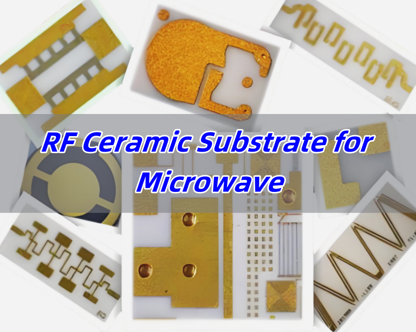
RF ceramic substrate is a key component for RF circuit and microwave circuit, it refers to a specialized ceramic material designed to support high-frequency circuits used in radio frequency systems. Unlike traditional materials, ceramic substrates used for RF circuits offer low signal loss, stable dielectric properties, and strong thermal resistance. It is usually made of alumina (Al₂O) ₃ ceramic material, with good insulation properties, high temperature stability and low dielectric loss characteristics, the dielectric constant is usually between 9-12, dielectric loss Angle is less than 0.0003.
Types of RF Ceramic Substrate
1. Alumina-Based Substrate
Alumina (Al2O3) is widely used for RF ceramic substrates because it offers high thermal conductivity, good mechanical strength, and stable dielectric behavior at high frequencies. It can handle both RF and microwave signals, making it suitable for communication systems, radar, and aerospace devices.
2. Aluminum Nitride (AlN) Substrate
Aluminum nitride offers both high thermal conductivity and lower dielectric constant compared to alumina. This helps improve signal integrity in high-speed circuits. AlN substrates work well in applications needing both heat dissipation and frequency stability, like power amplifiers and phased array antennas.
3. Beryllium Oxide (BeO) Substrate
BeO substrates provide the highest thermal conductivity among ceramic options. Although used less frequently due to handling concerns, BeO still finds use in specialized high-power RF systems where heat removal is critical.
RF Ceramic Substrate vs. Normal Ceramic Substrate
Not all ceramic substrates perform equally, especially when handling RF signals. Regular ceramic substrates, like those used in standard circuits, mainly focus on mechanical strength and insulation. Electrical performance, especially at high frequencies, often comes second.
RF ceramic substrates, however, prioritize electrical performance. They offer low dielectric loss, controlled dielectric constant, and tight tolerances, all of which ensure signals move smoothly without distortion. In microwave circuits, even minor changes in material properties can cause signal loss or unwanted interference. In addition to this, they are differ from materials composition and applications:
1. Material Composition
RF Ceramic Substrates: Typically made from Class I ceramic materials, including alumina (Al₂O₃), aluminum nitride (AlN), and silicon nitride (Si₃N₄). These materials offer good thermal conductivity, high-frequency performance, and excellent high-temperature stability.
Normal Ceramic Substrates: Primarily made from inorganic materials like alumina (Al₂O₃) and aluminum nitride (AlN). While these materials perform well at high temperatures, they do not match RF ceramic substrates in terms of high-frequency performance.
2. Application Fields
RF Ceramic Substrates: Primarily used in RF and microwave circuits, such as mobile communication base stations, broadcast transmitters, MRI coils, semiconductor RF power supplies, laser equipment, military radios, radar systems, and complete RF microwave devices. They are also used in power amplifiers, LC filters, transceiver modules, and microwave components.
Normal Ceramic Substrates: Widely used in high-power LED lighting, high-frequency communication, and railway power systems. They are valued for their excellent heat dissipation and high-temperature stability.
Benefits of RF Ceramic Substrate for Microwave
1. Low Dielectric Loss
RF ceramic substrates minimize signal loss at high frequencies, which helps maintain signal strength even across longer transmission paths.
2. Stable Dielectric Properties
Ceramic substrates keep their dielectric constant stable across wide temperature and frequency ranges.
3. Excellent Thermal Management
Microwave circuits often generate heat, especially at higher power levels. Ceramic substrates, particularly AlN and BeO, offer strong heat dissipation, it helps prevent thermal damage while preserving electrical performance.
4. Environmental Durability
Microwave systems used in aerospace, defense, and satellite applications face harsh environments, including vibration, radiation, and extreme temperatures. Ceramic substrates handle these conditions without losing mechanical or electrical reliability.
5. Precision Manufacturing
Ceramic substrates for RF circuits support fine-line patterns, which allows designers to create high-density circuits without losing signal integrity.
Ceramic Substrate HS Code
The HS code for ceramic substrates used in electronic circuits generally falls under 8547.10.00. However, for substrates specifically designed for RF or microwave circuits, local customs authorities may apply slight variations depending on composition, thickness, or intended use.
Well-Known RF Ceramic Substrate Brands
When choosing RF ceramic substrates, selecting reliable materials from established brands helps ensure consistent performance. Several companies specialize in developing high-performance ceramic materials specifically for RF and microwave applications. Below are some well-known names trusted across industries like telecom, aerospace, automotive radar, and satellite systems.
Rogers Corporation
Kyocera Fine Ceramics
Coorstek
Murata Manufacturing
Maruwa
NGK Spark Plug Co., Ltd.
Heraeus Electronics
At EBest Circuit (Best Technology), we offer customized RF ceramic PCBs for our customers, we have stable supply chain and enough stock in our warehouse. Therefore, we can handle time-sensitive orders and provide expedited service if you are urgent.
RF Ceramic Substrate Uses
Wireless communication modules like 5G antennas, RF front-end modules, and satellite communication devices.
Radar and sensing systems, including automotive radar, weather radar, and defense radar systems.
Aerospace and space electronics, such as satellite payloads, deep-space communication, and onboard electronics.
Medical imaging and equipment, including MRI and wireless telemetry devices.
Industrial RF Systems, like RF heating systems, test instruments, and high-frequency sensors.
RF Ceramic PCB Design Considerations
Designing RF ceramic PCBs requires a deep understanding of both high-frequency circuit behavior and ceramic material properties. Compared to standard FR4 or other organic substrates, ceramic materials handle RF signals differently, especially at microwave and millimeter-wave frequencies. Below are the key considerations to achieve stable signal transmission, low loss, and reliable performance.
1. Dielectric Constant and Its Stability
The dielectric constant (Dk) directly affects signal propagation speed and impedance matching. Ceramic substrates, such as Al₂O₃ or AlN, typically have Dk values ranging from 9 to 10 for Al2O3 and 8 to 9 for AlN. It’s not just about Dk itself but also its stability over frequency and temperature changes. For RF circuits, materials with minimal Dk variation across frequencies (up to 40 GHz and beyond) help maintain consistent phase and impedance control, which directly impacts signal integrity.
2. Loss Tangent (Df) and Signal Attenuation
Loss tangent (Df) measures how much energy the substrate material absorbs during signal transmission. Lower Df leads to less signal attenuation, especially at high frequencies.
For comparison, FR4’s Df can exceed 0.015 at 10 GHz, While a reliable data from Murata’s ceramic materials shows Df values around 0.0005 to 0.0010 at 10 GHz, which outperforms many organic substrates.
3. Conductor Surface Roughness
For microwave circuits, copper foil roughness directly affects insertion loss. Rougher copper increases conductor loss, especially above 10 GHz. Ceramic PCBs often use low-profile copper, with surface roughness below 2 µm (Rz), to minimize skin effect losses at high frequencies.
4. Coefficient of Thermal Expansion (CTE) Matching
Alumina substrates typically have a CTE around 6.5 ppm/°C, which aligns reasonably well with copper’s 17 ppm/°C when using proper bonding techniques. For applications like satellite communications, where temperature swings can exceed ±100°C, this balance ensures mechanical reliability.
5. Transmission Line Structures and Impedance Control
To design RF circuits on ceramic substrates, engineers often use microstrip, coplanar waveguide (CPW), or stripline structures. Achieving tight impedance control (±5% or better) requires precise trace width calculation, gap spacing, and accurate Dk data across the operating frequency range. For example, a 50-ohm microstrip line on 99.6% alumina with a 0.635 mm (25 mil) thickness requires a trace width around 1.5 mm, but the exact value shifts slightly based on the operating frequency and whether the substrate uses thin-film or thick-film copper.
6. Thermal Management for High-Power RF Circuits
High-power RF circuits, such as power amplifiers (PAs) or radar transmitters, generate considerable heat. Aluminum nitride (AlN) substrates, with thermal conductivity reaching 170 W/m·K, outperform alumina (20-25 W/m·K) by almost seven times. This high thermal conductivity helps dissipate heat efficiently, reducing thermal gradients that could detune RF circuits.
7. Via and Plating Quality
Plated vias connect RF traces between layers or serve as ground vias to improve EMI shielding. In RF ceramic PCBs, via diameters as small as 100 µm are common, especially in LTCC packages.
For more information about RF ceramic PCB design guide, welcome to contact us at sales@bestpcbs.com. We offer free technical support for any PCB frequent asked questions.
Why Choose EBest Circuit (Best Technology) as Your RF Ceramic PCB Supplier?
At EBest Circuit (Best Technology), we specialize in RF ceramic PCB manufacturing with over 18 years of experience serving global clients. We understand how critical dielectric stability, thermal management, and mechanical precision are for RF and microwave systems. Our in-house testing and quality checks ensure every board meets your performance standards, whether for 5G modules, radar systems, or aerospace electronics. At EBest Circuit (Best Technology), you can enjoy:
Products control under ISO13485, IATF16949, AS9100D system
Stable supply chain (cover various brands ceramic substrate)
Cutting edge technology for ceramic PCB manufacturing
Professional ceramic PCB engineer technical support
DDU & DDP quotation
2-3Weeks delivery
Highest quality
Customized RF ceramic PCB design
Turn-key service
With custom design support, quick turnaround, and flexible production options, we help clients bring RF innovations to market faster. Contact EBest Circuit (Best Technology) today to see how our RF ceramic PCB solutions can support your next project.
AlN PCB stands out as a top choice when companies need strong heat management and reliable performance in advanced electronics. This ceramic PCB substrate uses aluminum nitride, known for its high thermal conductivity and excellent electrical insulation. With electronics getting smaller and more powerful, keeping heat under control is more important than ever. That’s why many industries rely on AlN ceramic PCB to improve both performance and reliability.
At the same time, customers often want to know how AlN PCB fabrication works, how it compares to other options, and what affects its final price. Understanding these details helps engineers and buyers make smarter choices for their projects. In this blog, we’ll explore everything from the properties of aluminum nitride to the benefits, pricing factors, and even common assembly challenges.
If you’re searching for a reliable ceramic PCB substrate or want to understand how AlN PCB fits into your next design, this guide will help. Whether you’re working on high-frequency devices, power modules, or advanced communication systems, knowing the strengths of AlN PCB can make a big difference.
What is aluminum nitride PCB material?
AlN PCB stands for aluminum nitride PCB, which uses aluminum nitride ceramic as the base material. It is known for excellent thermal conductivity, strong electrical insulation, and reliability in harsh environments. Compared to standard FR4 boards, AlN PCB supports much better heat dissipation. That’s why engineers choose this material for high-power circuits, laser systems, and advanced communication devices.
Aluminum nitride acts as both the base and heat spreader. This unique structure reduces thermal stress, helping sensitive components stay cooler. As technology grows, more industries lean toward AlN PCB to handle performance needs.
Is aluminum nitride a ceramic?
Yes, aluminum nitride is a ceramic. It belongs to the advanced ceramic family, valued for its high strength, electrical insulation, and outstanding heat transfer abilities. Unlike traditional ceramic materials, aluminum nitride supports fast heat removal, which helps extend component life.
Since AlN is ceramic, it also resists chemicals, high temperatures, and mechanical wear. These benefits make it suitable for AlN ceramic PCB manufacturing. Today, designers rely on it for high-frequency devices, power electronics, and communication modules.
Is Aluminium nitride brittle?
Like other ceramics, aluminum nitride is somewhat brittle, especially under sudden mechanical shock. However, it still performs better than some other ceramics used in electronics. Proper design, combined with experienced fabrication techniques, helps reduce risks related to brittleness.
The good news is that once AlN PCB fabrication completes and the board is installed correctly, its durability is impressive. This balance of strength, heat management, and electrical insulation keeps AlN ceramic PCBs in high demand across industries like automotive, aerospace, and telecom.
How does AlN PCB compare to alumina PCB in thermal performance?
Thermal performance directly affects the reliability of modern electronics. When comparing AlN PCB to alumina PCB, aluminum nitride performs much better in heat transfer. Its thermal conductivity reaches around 170-200 W/mK, which is far higher than alumina’s 20-30 W/mK.
This major difference matters when components generate heat in compact spaces. Devices that push high power levels or require stable performance over time benefit from this advantage. While alumina PCB offers good insulation and is more affordable, AlN remains the first choice for heat-sensitive applications.
What is the difference between aluminum nitride PCB and aluminum PCB?
This is a common question from customers comparing materials. AlN PCB uses a ceramic core made from aluminum nitride, while aluminum PCB uses a metal aluminum base with a dielectric layer on top. Both manage heat, but they work in different ways.
AlN ceramic PCB offers excellent electrical insulation, which allows designers to place components closer together. It also handles extreme heat better without expanding too much. On the other hand, aluminum PCB, though cheaper, has limited electrical insulation, making it less suitable for high-frequency and precision circuits.
In short, AlN PCB fits better where thermal management and signal performance both matter. Aluminum PCB works well in simpler applications where cost matters more than advanced performance.
What factors affect AlN PCB price?
Several factors affect AlN PCB price, and understanding them helps customers plan projects better. First, the raw material cost plays a key role. Aluminum nitride is more expensive than standard PCB materials, but the benefits often outweigh the cost.
Next, fabrication complexity impacts price. Multilayer designs, micro vias, and precision routing need advanced technology, adding to the total. Batch size also matters. Larger runs usually lower the cost per piece, while small or custom orders cost more.
Lastly, surface treatment choices, tolerances, and assembly needs contribute to the final cost. That’s why working with an experienced AlN PCB fabrication supplier helps balance price and performance.
What are common PCB assembly issues with AlN ceramic PCBs?
Even with advanced materials like AlN ceramic PCB, assembly issues can happen without careful handling. One common challenge is matching the thermal expansion of components with the ceramic base. Sudden thermal changes can stress solder joints if not managed well.
Another potential issue comes from the surface finish. Choosing the wrong finish for high-frequency circuits or high-temperature processes can lead to signal loss or poor solderability.
Lastly, poor handling during assembly can crack the ceramic substrate. This highlights the importance of choosing experienced assembly partners with expertise in AlN PCB fabrication and assembly. By working with a trusted supplier, these risks can be minimized, improving reliability and performance.
What is the use of Aluminium nitride?
Aluminium nitride offers broad uses across multiple industries. Its high thermal conductivity makes it perfect for high-power electronics, such as laser drivers, RF amplifiers, and power modules. These systems generate heat that needs to move away quickly to protect components.
Besides electronics, AlN ceramic plays a role in NFC communication systems, where thermal stability and electrical insulation enhance performance. Medical devices also benefit from aluminum nitride’s biocompatibility and thermal management properties.
In short, AlN PCB supports applications that demand precise performance, stability, and long-term reliability, especially under demanding conditions.
How to select the right manufacturer for AlN PCB fabrication?
Selecting the right AlN PCB fabrication partner directly affects project success. Start by checking the manufacturer’s experience with ceramic PCB substrates. Not all PCB companies have the technology or skills to handle aluminum nitride.
Next, ask about in-house capabilities for drilling, plating, and precision routing. AlN requires specialized equipment and processes, so a capable supplier handles every step under one roof. This ensures quality control and reduces lead times.
Also, consider the manufacturer’s knowledge in PCB assembly issues, especially for ceramics. Experienced suppliers know how to manage thermal stress, select the right surface treatments, and optimize designs for both performance and manufacturability.
Finally, check for customer support and willingness to provide design advice. A good partner not only builds your boards but also helps improve designs to balance performance, cost, and reliability.
In a nutshell, choosing AlN PCB means investing in better thermal performance, electrical insulation, and reliability. With growing demand for aln ceramic pcb in high-power and high-frequency applications, more engineers turn to this advanced material.
Working with a professional AlN PCB fabrication partner ensures your boards meet both performance and cost goals. If you’re looking for a ceramic PCB substrate that can handle the heat, aluminum nitride offers one of the best options available.
At EBest Circuit (Best Technology), we specialize in advanced ceramic PCBs, including AlN inlay PCB, alumina PCB, and more. Our experts understand the challenges of aln pcb fabrication and assembly issues, delivering high-quality boards for demanding projects. For more information or inquiries, feel free to contact us at sales@bestpcbs.com.
Al2O3 ceramic PCB fabrication is the process of producing printed circuit boards using alumina (Al2O3) ceramic substrates. Alumina ceramics have high mechanical strength, hardness, heat resistance, electrical insulation and corrosion resistance, and are one of the most cost-effective materials in the electronic packaging industry.
Unlike ordinary PCBs, ceramic PCBs are made by directly bonding copper foil and ceramic substrates under high temperature environments. They have strong bonding strength, the copper foil will not fall off, and have high reliability and performance stability under high temperature and high humidity environments.
As a ceramic PCB manufacturer with 18 years of manufacturing experience, BEST Technology has accumulated rich professional strength in the manufacturing of alumina ceramic PCBs. In terms of manufacturing technology, it adopts advanced manufacturing processes to ensure that each alumina ceramic PCB meets high quality standards.
What is Alumina Ceramic PCB?
Alumina ceramic PCBs are circuit boards made using aluminum oxide (Al₂O₃) as the substrate material. This type of PCB is known for its excellent thermal management, high insulation resistance, and mechanical strength.
Compared to conventional FR-4 boards, alumina ceramic PCBs offer better heat dissipation, making them ideal for high-power applications like LED lighting, automotive electronics, and aerospace systems.
Unlike standard PCB materials, alumina ceramic is highly resistant to chemical corrosion and environmental stress. It can endure extreme temperatures without degrading, ensuring long-term reliability in demanding conditions.
How Do You Make Al₂O₃ Ceramic PCB?
Fabricating an alumina ceramic PCB requires a specialized manufacturing process. Unlike FR-4 boards, which are processed using laminates, ceramic PCBs are created through advanced sintering techniques.
The process typically involves:
Material Preparation – High-purity alumina ceramic is selected based on thermal and electrical requirements.
Substrate Formation – The ceramic is shaped and sintered at high temperatures to achieve a dense, strong structure.
Metallization – Copper, silver, or gold is deposited onto the ceramic surface using thick-film or thin-film technology.
Circuit Patterning – The conductive layer is etched or laser-processed to define the circuit layout.
Component Assembly – SMD or through-hole components are mounted using high-temperature soldering or wire bonding.
Final Testing – The finished PCB undergoes electrical and thermal testing to ensure optimal performance.
This fabrication method results in a robust, high-performance PCB with excellent electrical insulation and thermal efficiency.
What Are the Advantages of Alumina Ceramic PCB?
Al₂O₃ ceramic PCBs come with a range of benefits that make them superior to traditional materials.
Exceptional Heat Dissipation – The ceramic substrate effectively transfers heat away from components, preventing overheating.
High Mechanical Strength – Alumina ceramic is incredibly strong, resisting mechanical stress and impact.
Superior Electrical Insulation – This material prevents electrical leakage, ensuring stable circuit performance.
Corrosion Resistance – Unlike metal-based PCBs, alumina ceramic does not rust or degrade over time.
Dimensional Stability – It maintains its structure under extreme conditions, including high temperatures and humidity.
These advantages make alumina ceramic PCBs a top choice for advanced electronic applications requiring reliability and efficiency.
What Are the Materials Used in Ceramic Substrate?
Ceramic PCBs can be made using different types of ceramics, each offering unique properties:
Alumina (Al₂O₃) – The most widely used ceramic material, known for its affordability and strong thermal performance.
Aluminum Nitride (AlN) – Offers higher thermal conductivity than alumina but comes at a higher cost.
Beryllium Oxide (BeO) – Provides outstanding thermal properties but has limited use due to toxicity concerns.
Silicon Carbide (SiC) – Used in specialized high-temperature applications.
Each material is selected based on specific electrical, thermal, and mechanical requirements.
Is Alumina Ceramic Better Than Zirconia Ceramic?
Alumina and zirconia ceramics are both high-performance materials, but they serve different purposes.
Alumina Ceramic (Al₂O₃) – Offers better thermal conductivity, making it ideal for PCBs that require efficient heat dissipation.
Zirconia Ceramic (ZrO₂) – Has superior mechanical toughness and is often used in wear-resistant applications.
For electronic circuit boards, alumina is the preferred choice due to its balance of strength, electrical insulation, and heat management.
How Thick is Alumina Ceramic PCB?
The thickness of an alumina ceramic PCB varies based on application needs. Typically, the substrate thickness ranges from 0.25mm to 5mm, depending on thermal and mechanical requirements.
Thinner PCBs are used in compact electronics, while thicker substrates are chosen for heavy-duty applications requiring robust performance.
What is the Difference Between Al₂O₃ Ceramic PCB and FR-4?
FR-4 and alumina ceramic PCBs are widely used, but they differ in key ways:
Material Composition – FR-4 is a fiberglass-reinforced epoxy, while alumina ceramic is a solid ceramic substrate.
Thermal Conductivity – Alumina ceramic dissipates heat much more efficiently than FR-4.
Durability – Ceramic PCBs can withstand harsh environments, whereas FR-4 boards are more prone to degradation.
Electrical Performance – Alumina has superior insulation and minimal signal loss, making it ideal for high-frequency circuits.
For applications where heat management and longevity are critical, alumina ceramic PCBs offer a clear advantage.
What Are the Applications of Alumina Ceramic PCB?
Due to their exceptional properties, alumina ceramic PCBs are used in various industries:
LED Lighting – Ensures efficient heat dissipation for high-brightness LEDs.
Power Electronics – Used in high-voltage circuits requiring stability and durability.
Automotive Electronics – Found in electric vehicles, sensors, and power management systems.
Aerospace & Defense – Used in radar, communication, and avionics due to reliability under extreme conditions.
Medical Devices – Integrated into imaging systems and surgical instruments for their biocompatibility and precision.
As electronic devices continue to demand higher efficiency and performance, alumina ceramic PCBs are becoming an essential part of modern technology.
Conclusion:
Al₂O₃ ceramic PCBs provide a superior solution for applications requiring durability, thermal efficiency, and electrical reliability. Compared to traditional FR-4 boards, they offer better heat dissipation, mechanical strength, and longevity.
For high-quality alumina ceramic PCB fabrication, choosing the right manufacturer is crucial. At EBest Circuit (Best Technology), we specialize in custom ceramic PCBs designed to meet the most demanding requirements. Contact us at sales@bestpcbs.com to discuss your project needs!
When people talk about high-frequency ceramic PCB for antenna, they often focus on two things: the material and the performance. This type of PCB uses ceramic-based substrates instead of standard materials like FR4. Ceramic materials handle high frequencies much better, which is why they are widely used in antennas, especially for advanced communication systems.
Ceramic PCBs are different because they have excellent thermal properties, stable performance across various temperatures, and a low dielectric loss. When designing antennas, stable signal transmission matters a lot. If the PCB can’t hold signals well, the antenna won’t perform as expected. That’s where ceramic PCBs shine. They can work reliably at frequencies over 1GHz, even reaching into the millimeter-wave range.
For antennas, precision and stability are key. High-frequency ceramic PCBs offer low signal loss, better impedance control, and excellent high-speed signal transmission. Compared to other materials, they help antennas work more efficiently, even in complex environments.
Raw Materials of High-Frequency Ceramic PCB
The materials used in high-frequency ceramic PCB for antenna directly impact performance. Ceramic PCBs rely on substrates like Alumina (Al2O3), Aluminum Nitride (AlN), and Beryllium Oxide (BeO). Each has special properties that match specific antenna needs.
Alumina is popular for its balance between cost and performance. It has stable electrical properties, good thermal conductivity, and works well with various frequencies.
Aluminum Nitride provides higher thermal conductivity than Alumina, which helps when antennas run in high-power or high-heat situations.
Beryllium Oxide offers even better thermal properties, but it’s used less due to its handling restrictions.
Ceramic PCBs also use conductive materials like silver, gold, or copper, depending on the frequency and environment needs. The right combination of ceramic substrate and conductor helps antennas maintain low signal loss and high reliability, even under extreme conditions.
Advantages of Ceramic PCB Used in Antenna
Using high-frequency ceramic PCB for antenna provides many benefits, especially when high performance matters. These advantages help designers build better antennas that stay stable over time, make them in a smart choice for antennas in 5G, radar, GPS, and satellite communication systems.
Low dielectric loss: Signals travel through ceramic with less loss, which helps antennas work better at high frequencies.
Stable performance: Ceramic PCBs handle temperature changes, moisture, and mechanical stress well. That stability matters for outdoor antennas or systems working in tough environments.
Excellent thermal management: Antennas, especially those handling strong signals, produce heat. Ceramic spreads heat faster than traditional materials, which helps antennas work longer without performance drops.
Higher frequency support: Standard PCBs struggle with frequencies above a few GHz. Ceramic PCBs handle millimeter-wave frequencies better, making them ideal for advanced communication systems.
Tighter tolerances: Ceramic PCBs can be made with more precise dimensions, which helps match the antenna’s electrical design closely. This precision supports better impedance control.
Longer lifespan: Ceramic resists wear, corrosion, and aging better than many organic materials. That means antennas using ceramic PCBs tend to last longer.
High-Frequency Ceramic PCB vs. High-Frequency PCB
It’s common to hear people compare high-frequency ceramic PCB for antenna with standard high-frequency PCB. Both support high-speed signals, but they serve different purposes.
1. Material difference:
High-frequency PCBs often use PTFE, hydrocarbon, or special composite materials. Ceramic PCBs use Rogers Alumina, Aluminum Nitride, or similar ceramics.
2. Thermal performance:
Ceramic spreads heat much faster than PTFE or composites, helping antennas in high-power systems.
3. Dielectric loss:
Ceramic PCBs generally have lower dielectric loss at high frequencies, which helps antennas maintain signal clarity.
4. Mechanical stability:
Ceramic is rigid and doesn’t change shape much with temperature or moisture. Some high-frequency laminates can swell or shrink, which affects signal paths.
5. Frequency range:
While both support GHz-level signals, ceramic handles higher frequencies more easily, including millimeter-wave bands.
In short, high-frequency ceramic PCBs work best when both thermal performance and high-frequency stability matter. Standard high-frequency PCBs work well for simpler systems, but antennas pushing into higher frequencies often rely on ceramic for better results.
Design Considerations for High-Frequency Ceramic PCB
Designing a high-frequency ceramic PCB for antenna involves more than choosing the right materials. Several factors impact performance, so careful attention at the design stage helps prevent later problems.
1. Substrate choice: Picking the right ceramic type depends on frequency, heat load, and physical size. Higher frequencies need materials with lower dielectric loss, while high-power antennas need better thermal conductivity.
2. Avoid crosstalk: It is best to use a straight line or 45degree traces to reduce the transmission of high frequency signals and mutual coupling. Parallel routing in a close distance may cause crosstalk.
3. Impedance control: Maintaining accurate impedance across the whole PCB keeps signals clean. Ceramic’s stable properties help, but the design must account for it too.
4. Via design: For multi-layer designs, vias must maintain low loss and good grounding. Plated vias, filled vias, or even embedded vias help control high-frequency signals.
5. Grounding strategy: Good grounding keeps signals clean and reduces unwanted noise. Ground planes should be carefully placed and connected to avoid signal interference.
6. Thermal management: Heat buildup changes performance over time. Even though ceramic handles heat better than FR4, the layout should still allow heat to spread efficiently.
When all these factors work together, the final antenna performs better, holds signal quality longer, and operates reliably under real-world conditions.
When choosing a high-frequency ceramic PCB for antenna, working with an experienced manufacturer makes a real difference. EBest Circuit (Best Technology), with more than 18 years of PCB manufacturing experience, specializes in high-frequency ceramic PCBs designed for antennas in various industries.
We work with top-grade ceramic materials like Dupont, Rogers, Isola, etc. to meet the demands of advanced communication systems. Our team works closely with customers to match the right material and design to each antenna’s frequency range, power level, and environment.
We also offer precision manufacturing processes to keep line widths, spacing, and via placements within the tight tolerances high-frequency designs need. Whether your antenna supports 5G, satellite communications, or radar systems, we deliver reliable, high-performance ceramic PCBs that keep signals clean and strong.
With advanced testing, rigid quality control, and a customer-first approach, we help companies build better antennas faster. Contact EBest Circuit (Best Technology) today to explore how our high-frequency ceramic PCBs can improve your next antenna project.
FAQs of High Frequency Ceramic PCB
Q1: Why use ceramic PCBs for high-frequency antennas?
Ceramic PCBs offer lower signal loss, better thermal management, and more stable performance at high frequencies than traditional materials.
Q2: Which ceramic materials work best for antenna PCBs?
Alumina, Aluminum, Nitride are popular choices. Each supports different frequencies and heat loads.
Q3: Are ceramic PCBs suitable for 5G antennas?
Yes, they support the millimeter-wave frequencies used in 5G networks, along with excellent signal integrity.
Q4: Do ceramic PCBs cost more than regular high-frequency PCBs?
They often cost more initially, but their longer lifespan and better performance provide good value.
Q5: Can ceramic PCBs handle outdoor conditions?
Yes, ceramic resists moisture, temperature changes, and mechanical stress better than many organic materials.