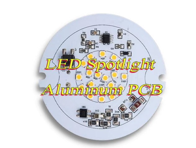
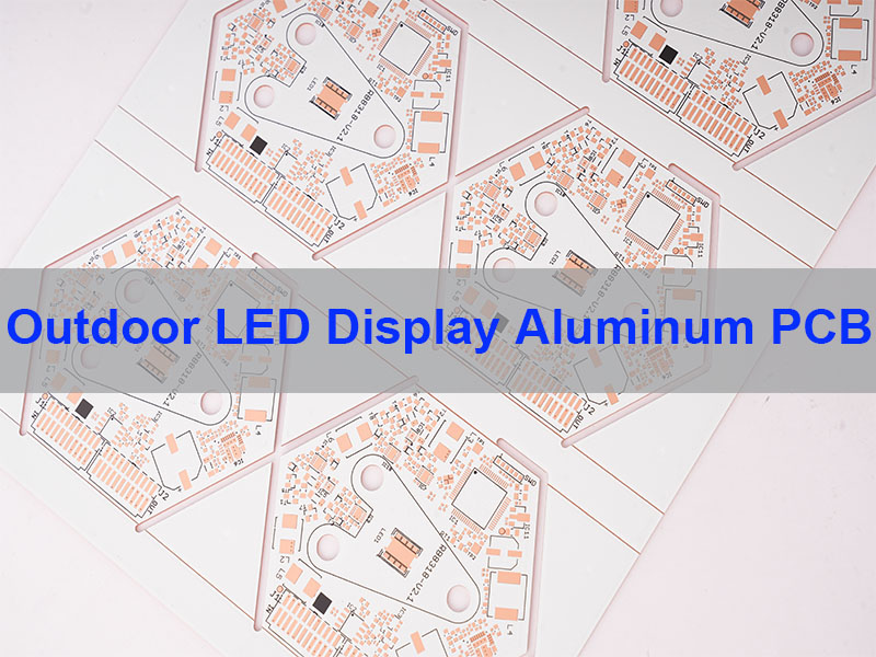
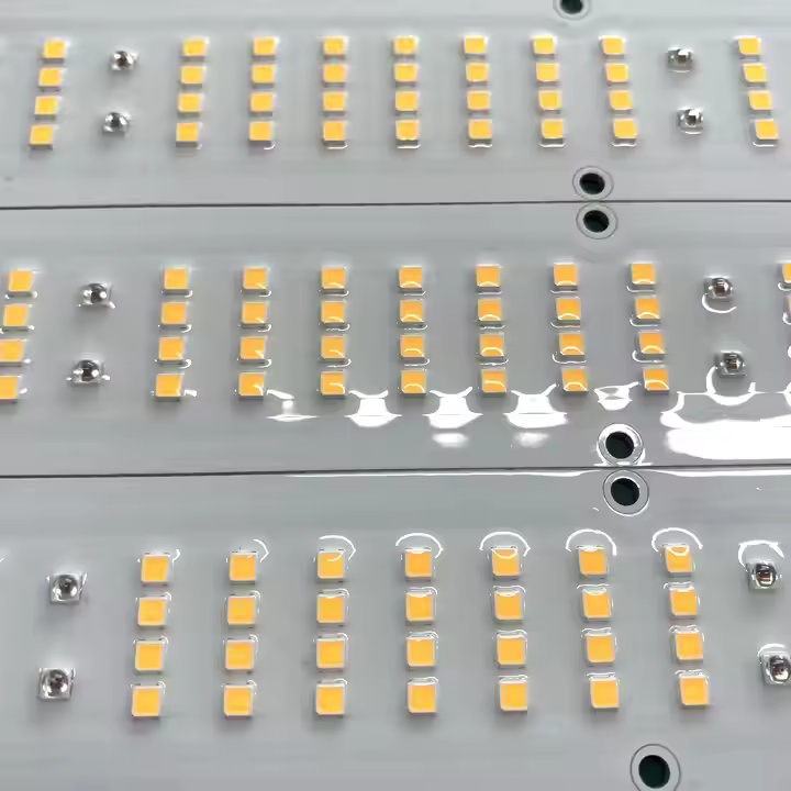
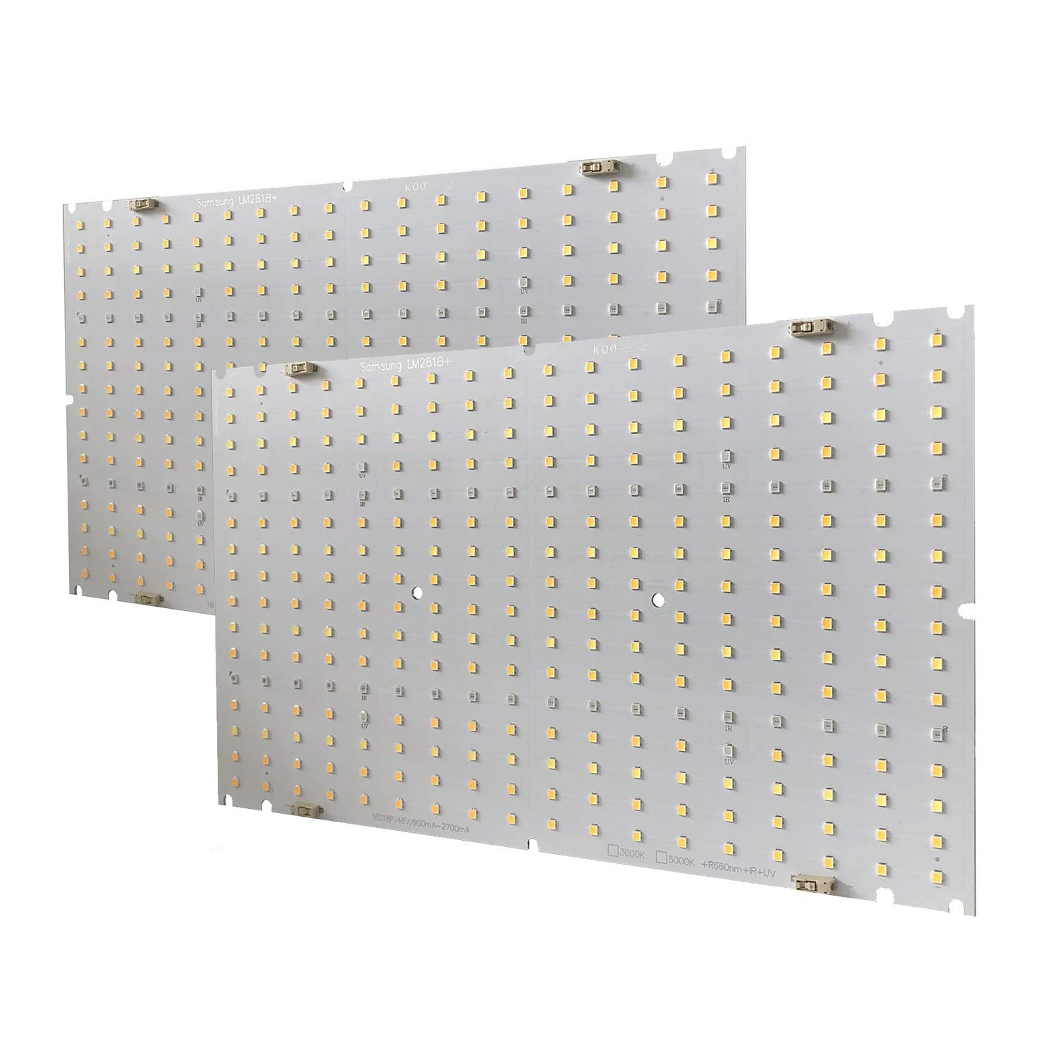
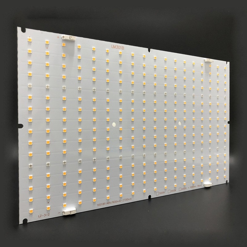
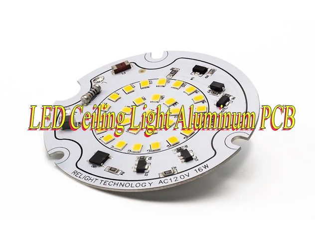
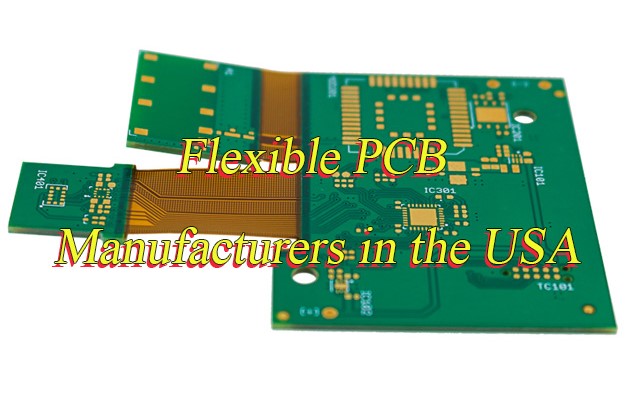
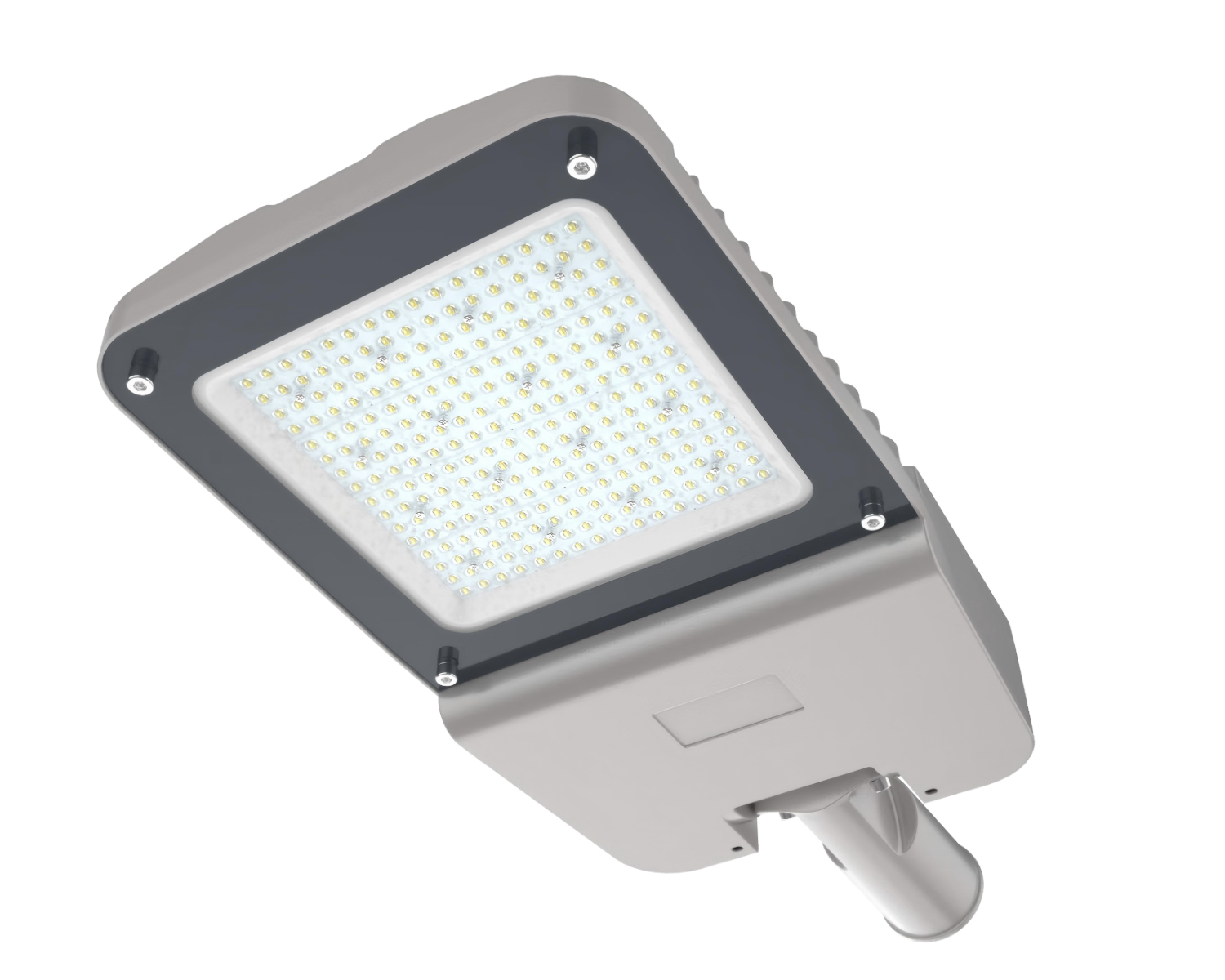
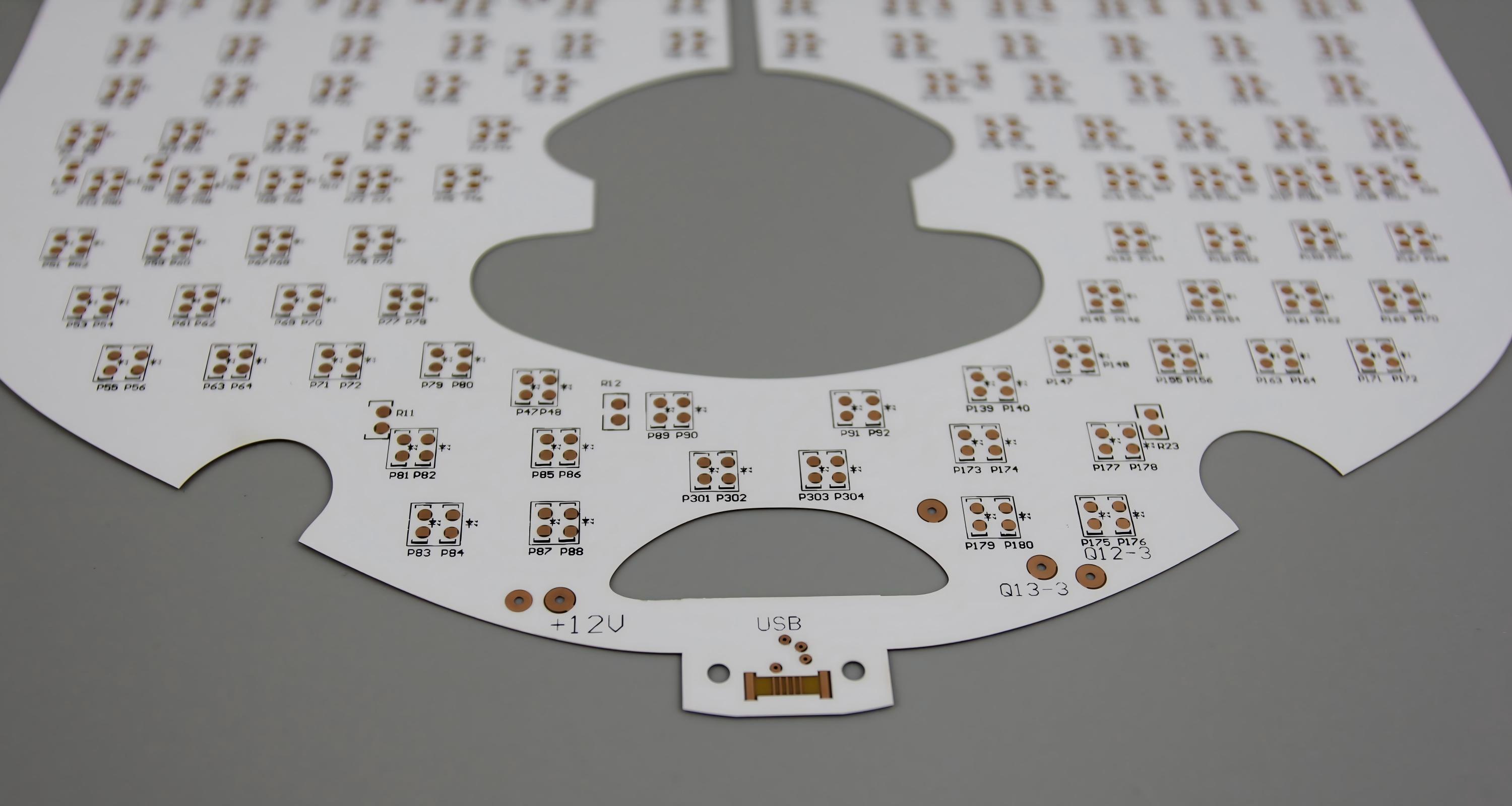
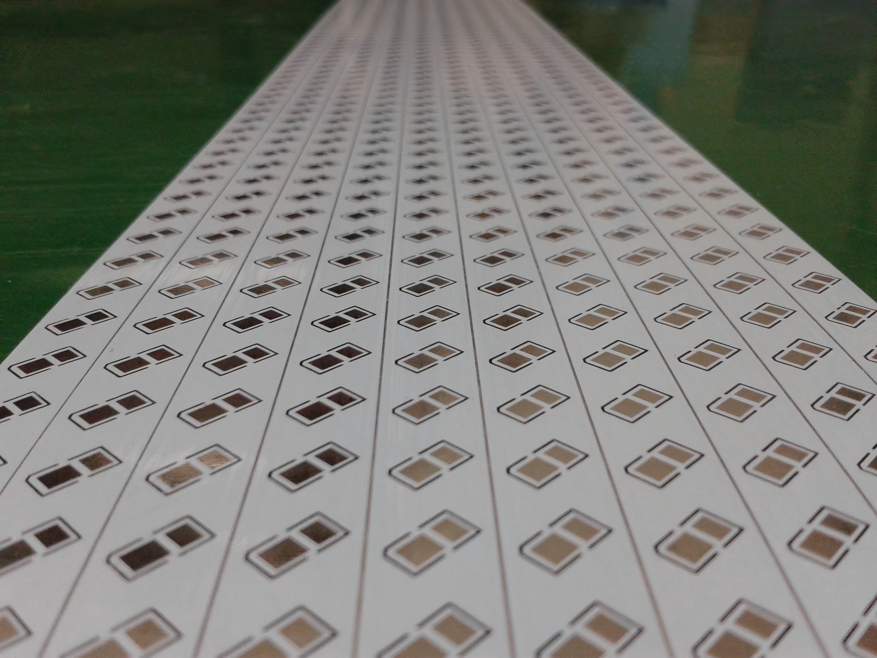
Indoor LED Display Aluminum PCB is a metal-core printed circuit board designed for indoor LED display modules, using an aluminum base to improve heat dissipation, enhance structural stability, and support reliable long-term display performance.
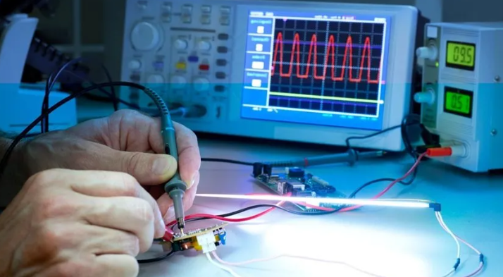
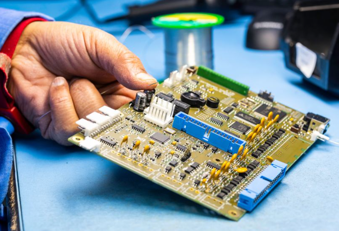
At EBest Circuit (Best Technology), we provide Indoor LED Display Aluminum PCB manufacturing with engineering support, fast response, and production control for stable indoor LED applications. We support customers who need dependable heat spreading, solid soldering performance, and repeatable quality for batch orders.
Core parameters customers often ask for
- Base material aluminum core / metal core structure
- Copper thickness 1oz, 2oz, or project-based design
- Board thickness custom according to module structure
- Thermal dielectric selected for indoor LED heat transfer needs
- Surface finish HASL, ENIG, OSP, or project requirement
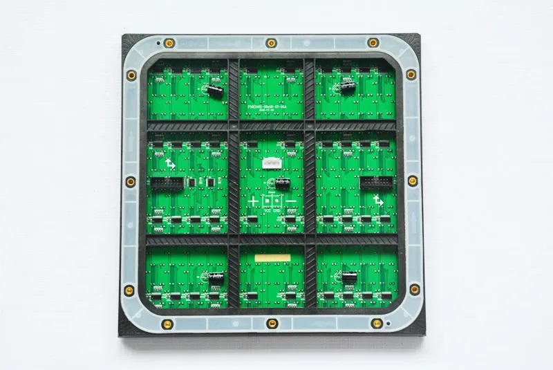
- Application indoor fine-pitch LED modules, meeting room displays, commercial indoor screens
Why choose us for this product
- Quality controlled fabrication and assembly process for stable display modules
- Lead time responsive support from sampling to volume builds
- Service engineering communication that focuses on manufacturability and project fit
- Supply continuity one-stop coordination for PCB fabrication and related assembly support
Therefore, a well-built aluminum PCB is not just a substrate choice, but the thermal foundation of indoor LED display reliability. In practice, buyers who start from board structure usually reduce downstream instability in the full module build.
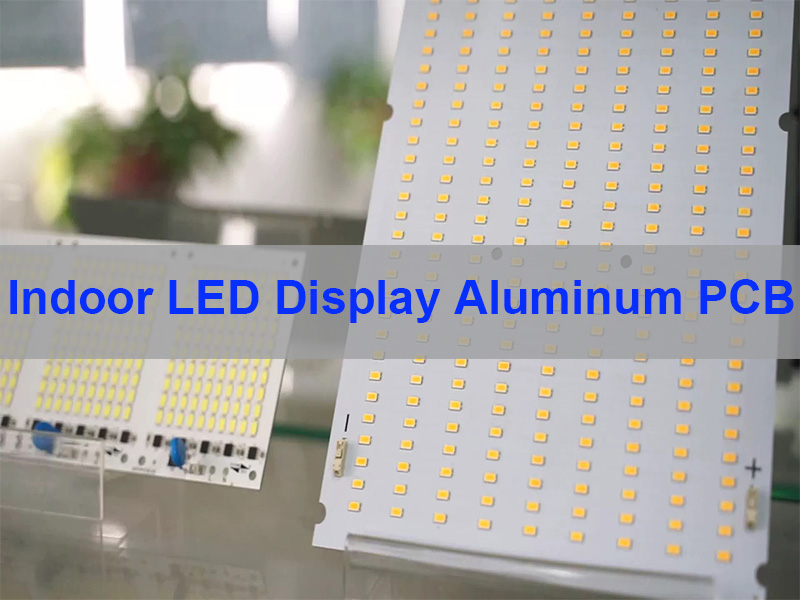
What Is an Indoor LED Display Aluminum PCB and How Does It Work?
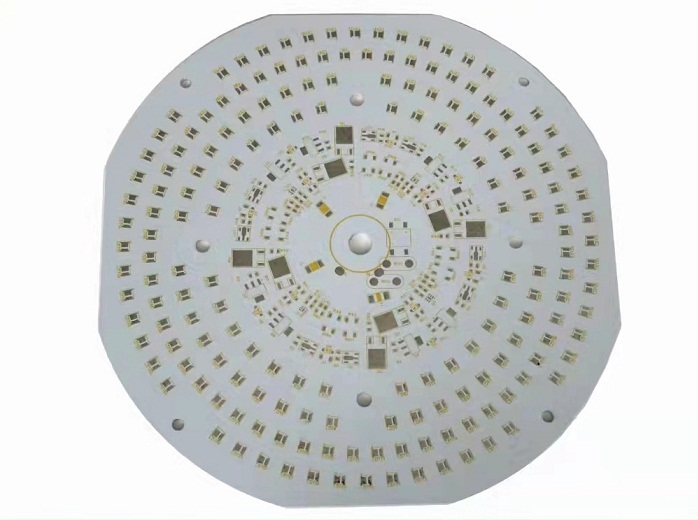
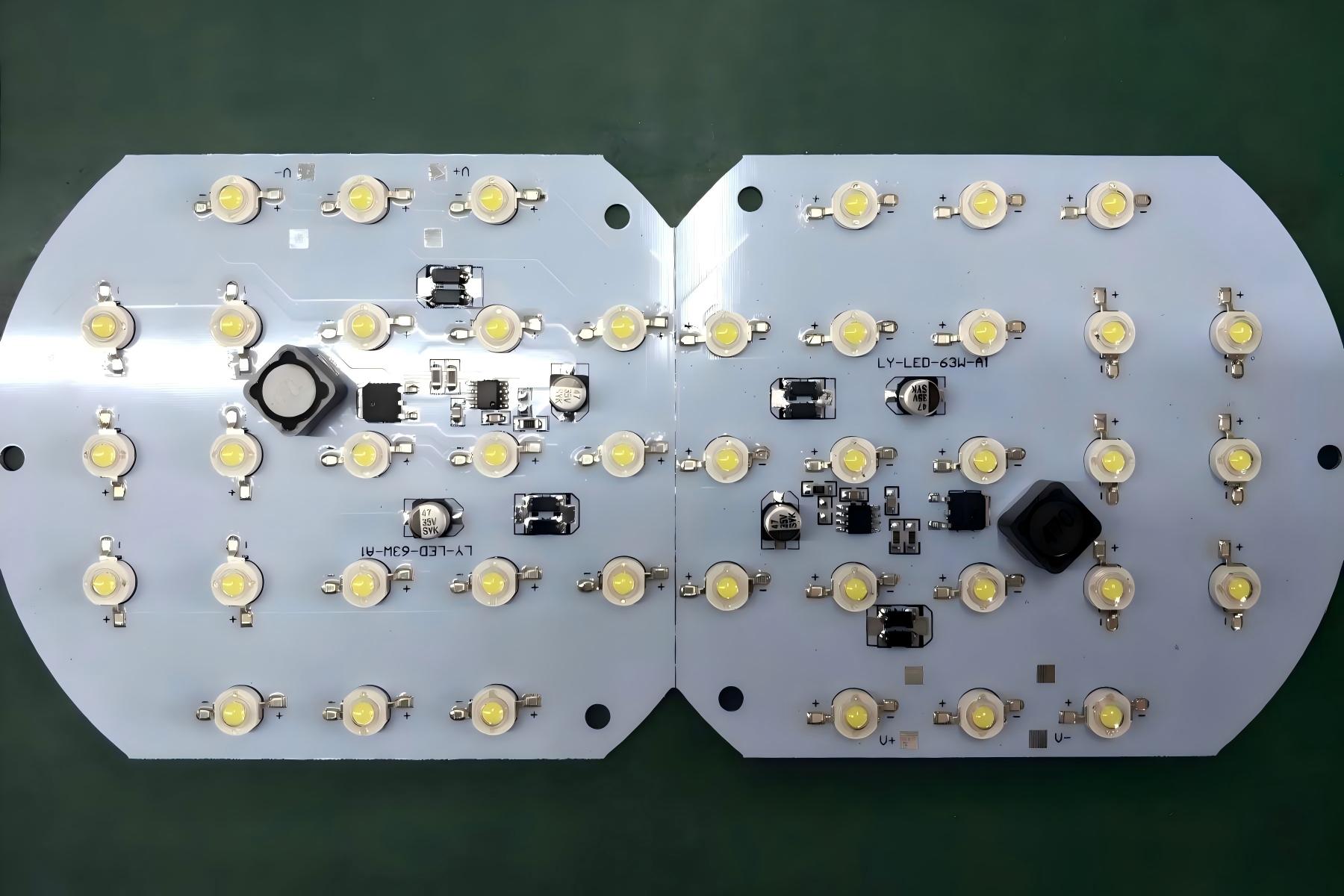
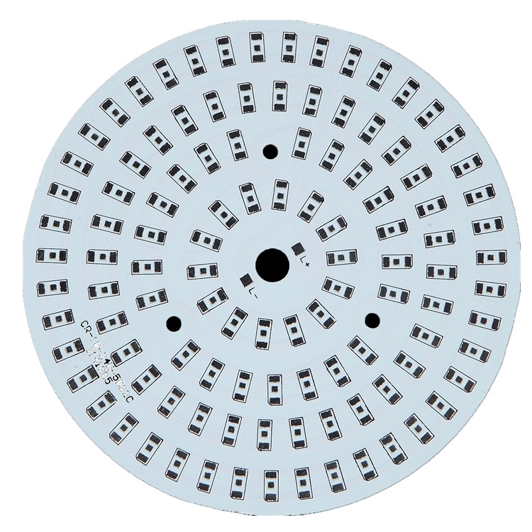
An Indoor LED Display Aluminum PCB is a metal-core circuit board designed to carry LED packages and related circuitry while moving heat away from the light source more efficiently than a standard FR4 board. It typically includes a copper circuit layer, a thermally conductive dielectric layer, and an aluminum base that spreads heat across a wider area.
For indoor LED displays, this structure matters because dense LED layouts can create local heat concentration. When heat is guided away quickly, the display is more likely to keep stable brightness, cleaner color performance, and longer service life.
Basic structure
| Layer | Function | Why It Matters for Indoor LED Displays |
|---|---|---|
| Copper Circuit Layer | Carries current and signal paths | Supports LED connection stability and layout accuracy |
| Thermal Dielectric Layer | Transfers heat while keeping electrical insulation | Helps control heat flow from LEDs to the base |
| Aluminum Base | Spreads and releases heat | Improves thermal balance and mechanical support |
Overall, this board type is chosen when thermal control and dimensional stability matter as much as electrical connectivity. This means it is especially suitable for indoor LED modules expected to run for long periods in conference and presentation environments.
Why Is Aluminum Better Than Standard FR4 for Indoor LED Display Thermal Control?
For many indoor LED display projects, aluminum offers a more practical thermal path than standard FR4 because it spreads heat faster and supports better mechanical rigidity. This is especially valuable in fine-pitch or high-density indoor displays where localized heating can affect both image quality and solder joint life.
FR4 still works in many electronics, but indoor LED display modules often benefit from the metal-core approach when brightness stability and long operating time are priorities. Aluminum also helps support flatter panel construction, which is useful when multiple modules must align into one seamless display surface.
Aluminum PCB vs FR4 for indoor LED display use
| Item | Aluminum PCB for Indoor LED Display | Standard FR4 PCB |
|---|---|---|
| Heat spreading | Strong | Moderate |
| Suitability for dense LED arrays | High | Lower in thermal-heavy designs |
| Board rigidity | Better mechanical support | General-purpose support |
| Risk of thermal accumulation | Reduced with correct stack-up | Higher in high-density LED zones |
| Fit for quiet indoor display design | Very suitable | More limited in passive thermal design |
As a result, aluminum is often the safer choice when the display must stay visually stable without relying heavily on extra cooling methods. From an engineering perspective, that makes the board itself part of the thermal solution rather than just a wiring platform.
How Does an Aluminum PCB Improve Meeting Room LED Display Performance?
In meeting rooms, the display is viewed at close distance, often for long sessions, so thermal consistency directly affects visual experience. A better thermal base helps the screen keep uniform brightness, cleaner white balance, and lower risk of color variation across modules.
It also supports quieter system design. Many indoor meeting room displays prefer passive or low-noise thermal strategies, and a well-designed Aluminum PCB for Indoor LED Display helps make that possible.
Performance gains that matter in meeting rooms
- More stable brightness during long presentations
- Lower thermal stress on LED packages and solder joints
- Better module flatness for close-view visual consistency
- Reduced chance of hotspots in dense pixel layouts
- Improved fit for quiet indoor environments
In real-world applications, meeting room screens are judged by visual comfort as much as technical output. Notably, thermal control at the PCB level helps support both at the same time.
What Pain Points Do Buyers Face with Indoor Aluminum PCB LED Display Projects?
Buyers usually do not struggle with naming the product. They struggle with whether the board will stay stable after assembly, run cool enough in dense layouts, and remain consistent across batches. The most repeated concerns are warpage, poor heat flow, solder fatigue, uneven brightness, and production inconsistency from one build lot to another.
These issues often appear when the substrate choice, dielectric performance, copper design, and assembly process are not aligned from the start. That is why many indoor LED projects fail quietly during long operation, not during first power-on testing.
Common pain points and how we address them
| Pain Point | What It Causes | How EBest Circuit Helps |
|---|---|---|
| Heat buildup in dense LED areas | Brightness drift and shorter life | Thermal-focused stack-up and process review |
| Board warpage or flatness variation | Poor module alignment and visual inconsistency | Controlled fabrication and dimensional inspection |
| Solder joint stress | Intermittent failures over time | Process control for stable assembly compatibility |
| Batch-to-batch inconsistency | Mixed display performance across modules | Standardized production control and traceable workflow |
| Unclear technical support | Design delays and manufacturability issues | Engineering communication before mass build |
In short, the biggest risk is not one dramatic defect, but many small inconsistencies adding up in the finished display wall. To sum up, choosing a supplier that understands both PCB fabrication and LED display application logic helps prevent that chain reaction.
How Should PCB Aluminum for Indoor LED Display Be Designed for Better Heat Dissipation?
The answer is to treat thermal design as a full-board system, not a single material choice. A strong PCB Aluminum for Indoor LED Display design combines the right base thickness, proper dielectric selection, current path planning, copper balance, LED spacing, and interface design with the module frame or cabinet.
Many overheating problems come from poor heat path continuity. Even if the board uses aluminum, the result will be limited if copper distribution is uneven, thermal bottlenecks remain near LED clusters, or module contact to the supporting structure is weak.
Design focus areas
- Keep heat-generating LEDs evenly distributed where possible
- Use copper layout that supports both current carrying and heat spreading
- Avoid sharp local thermal concentration under dense pixel zones
- Match board flatness needs with module and frame requirements
- Consider assembly process compatibility from the layout stage
Recommended design checkpoints
| Checkpoint | Why It Matters |
|---|---|
| Dielectric thermal performance | Controls how effectively heat moves to the aluminum base |
| Copper balance | Supports thermal spreading and dimensional stability |
| LED package spacing | Reduces hotspot concentration |
| Panel flatness | Helps maintain seamless indoor display alignment |
| Assembly compatibility | Improves solder reliability and production repeatability |
Meanwhile, the best thermal result usually comes from coordinated board and mechanical design rather than isolated PCB optimization. This means the aluminum substrate should be planned as part of the full display module architecture.
How Do We Manufacture LED Display Indoor Aluminum PCB for Stable Quality?
Stable manufacturing begins with material control and continues through imaging, etching, lamination, profile control, surface finishing, and final inspection. For LED Display Indoor Aluminum PCB products, process discipline is important because indoor LED modules require both thermal function and dimensional consistency.
Even small process variation can affect flatness, solderability, or thermal transfer behavior. That is why a production flow for LED display aluminum boards must focus on repeatability, not just output speed.
Typical manufacturing flow
- Material confirmation based on thermal and structural requirement
- Circuit pattern creation and copper processing
- Dielectric and base structure control
- Drilling, routing, and profile shaping
- Surface finish selection for assembly compatibility
- Electrical and dimensional inspection
- Packing protection for safe shipment and module assembly readiness
What we pay special attention to
- Dimensional stability across batches
- Clean surface condition for reliable assembly
- Flatness control for seamless module installation
- Traceable production workflow for project consistency
From a manufacturing standpoint, indoor LED boards require consistency more than visual complexity. In practical terms, that consistency is what protects the final display from uneven module behavior after installation.
What Services and Certifications Should You Expect from an Indoor LED Aluminum PCB Supplier?
A capable supplier should provide more than bare board fabrication. You should expect technical communication, project review, documentation support, quality traceability, and clear manufacturing control for indoor LED applications. Certifications also matter because they indicate that the quality system is managed, repeatable, and suitable for customers who need dependable supply.
At EBest Circuit (Best Technology), we support LED-related PCB and PCBA projects with coordinated service from inquiry to delivery. For customers building Indoor Aluminum PCB LED Display products, this reduces handoff friction and helps keep engineering and production aligned.
Our service scope
| Service Item | What It Supports |
|---|---|
| PCB fabrication | Aluminum and application-matched board manufacturing |
| Engineering review | Manufacturability and project feasibility check |
| Assembly support | Better connection between bare board and final product build |
| Project communication | Faster clarification of drawings and production needs |
| Traceable workflow | Improved batch control and follow-up support |
Certificates
| Certificate | What It Signals |
|---|---|
| ISO 9001 | Managed quality system |
| ISO 13485 | Controlled quality practices for medical-related manufacturing environments |
| IATF 16949 | Automotive-oriented process discipline |
| AS9100D | Aerospace-oriented quality management capability |
| RoHS / REACH compliance support | Material and regulatory alignment for many global projects |
Likewise, certifications alone do not guarantee a good project result, but they do show whether the supplier is operating with structured control. For buyers, that structure often translates into more predictable performance and smoother communication.
What Related Questions Do Buyers Commonly Ask Before Ordering Aluminum Indoor LED Display PCB?
Before placing an order, most buyers ask practical questions rather than abstract ones. They want to know which stack-up fits indoor fine-pitch modules, how flat the board can stay, whether the surface finish supports reliable assembly, and how to match the board to the module frame and display cabinet.
These questions are useful because they reveal the real success criteria of the project. A good supplier should answer them clearly before production starts.
High-interest questions often asked during inquiry
- What board structure is best for indoor fine-pitch LED modules?
- How do you control flatness for seamless indoor display assembly?
- Which surface finish is better for LED module soldering?
- How do you verify thermal performance in a dense LED layout?
- Can the board design support long daily operating hours?
- How do you maintain consistency across repeat production lots?
Besides, clear answers at the inquiry stage usually reduce revision loops later in the project. In engineering terms, early question quality often predicts final manufacturing smoothness.
How Does Display Indoor LED Aluminum PCB Support Long-Term Reliability?
Long-term reliability comes from controlling temperature, stress, and process variation together. A Display Indoor LED Aluminum PCB improves the first part by giving heat a faster path away from LEDs, but the full reliability result also depends on flatness control, soldering compatibility, and consistent material behavior over time.
When these factors work together, the display is more likely to maintain image uniformity and resist gradual degradation during long operation cycles. That matters in meeting rooms where the display must look stable every day, not only during initial testing.
Reliability factors linked to board design
| Reliability Factor | Board-Level Impact |
|---|---|
| Heat control | Helps reduce LED aging speed |
| Mechanical stability | Supports better module alignment |
| Solder compatibility | Improves joint integrity over long use |
| Batch consistency | Keeps screen performance more uniform |
| Clean manufacturing | Reduces hidden process-related failure risk |
By comparison, a board chosen only for basic connectivity may pass early testing but create hidden weakness later. Hence, reliability in indoor LED display projects should be designed into the substrate from the beginning.
What Are the Best Application Cases for Aluminum Indoor LED Display PCB?
The strongest application cases are indoor environments that demand close viewing, long operating time, and strong visual consistency. In these settings, Aluminum Indoor LED Display PCB products help support cleaner thermal performance and better screen stability than many standard board approaches.
Four industries stand out because they depend heavily on indoor display clarity and operating consistency. These examples also show why the board choice matters at the system level.
Typical industry cases
| Industry | Typical Use | Why Aluminum PCB Helps |
|---|---|---|
| Corporate Meeting Rooms | Presentation walls and boardroom screens | Supports stable brightness and quiet thermal behavior |
| Control Rooms | Continuous-operation monitoring displays | Improves long-run thermal stability and screen consistency |
| Retail and Showrooms | Indoor branding and product presentation walls | Helps maintain visual uniformity during long opening hours |
| Education and Training Spaces | Lecture screens and collaborative display systems | Provides reliable operation for repeated daily use |
Example use case
A fine-pitch indoor conference display with long daily operating time usually needs more than visual resolution. It also needs a board that supports uniform heat spreading across many closely packed LEDs, especially when the system is expected to remain quiet and visually consistent during extended meetings.
Ultimately, the best application is any indoor LED display where stable image quality matters over time. For that reason, aluminum PCB structures are often selected in projects that value both visual precision and operational confidence.
How Should You Choose the Right Supplier for LED Indoor Display Aluminum PCB?
You should choose a supplier that understands how PCB fabrication affects final display behavior. That means the supplier should be able to discuss thermal structure, flatness, copper design, assembly compatibility, process consistency, and project documentation with confidence.
A strong supplier is not only a factory. It is also a technical partner that can identify hidden manufacturability risks before they turn into module instability or field complaints.
What to evaluate during supplier selection
- Experience with LED-related thermal board applications
- Ability to communicate technical details clearly
- Consistency in fabrication control and inspection
- Support for repeat production with stable quality
- Service response during design and order preparation
- Quality system and certification visibility
Why many customers choose us
EBest Circuit (Best Technology) combines PCB manufacturing capability with application-focused support for demanding projects. For buyers of LED Indoor Display Aluminum PCB, that means smoother technical discussion, controlled production, and a stronger path from drawing to delivery.
Correspondingly, the right supplier helps reduce technical uncertainty before the first production lot begins. Overall, that is one of the most valuable advantages in indoor LED display manufacturing. If you are looking for a dependable supplier for Indoor LED Display Aluminum PCB, EBest Circuit (Best Technology) is ready to support your project. We provide professional Indoor LED Display Aluminum PCB products for indoor display applications. For inquiries and orders, pls feel free to contact us at sales@bestpcbs.com.
FAQs About Indoor LED Display Aluminum PCB
How does Indoor Aluminum PCB LED Display improve thermal performance?
It improves performance by transferring heat from the copper layer through a thermally conductive dielectric into the aluminum base, where heat can spread more efficiently. This helps reduce hotspot buildup and supports more stable long-term display operation.
Why use LED Display Indoor Aluminum PCB in meeting room screens?
Meeting room displays are viewed at short distance and often run for long sessions, so thermal stability directly affects image uniformity and reliability. Aluminum PCB structures help support quiet operation, stable brightness, and better module flatness.
How do you choose PCB Aluminum for Indoor LED Display?
Start by checking thermal requirements, LED density, board thickness, copper design, assembly compatibility, and flatness needs. The right choice is the one that matches both the electrical design and the mechanical structure of the display module.
What is the difference between FR4 and Indoor LED Aluminum PCB Display?
FR4 is a general-purpose substrate, while aluminum PCB includes a metal base that spreads heat more effectively. For indoor LED display modules with dense LED layouts, aluminum usually offers stronger thermal support and better dimensional stability.
How can EBest Circuit support Display LED Indoor Aluminum PCB projects?
We support customers with PCB fabrication, engineering communication, controlled production workflow, and quality-focused service for indoor LED applications. This helps reduce manufacturing risk and improves consistency from sample stage to repeat orders.
Can Aluminum Indoor LED Display PCB support long operating hours?
Yes, when the stack-up, dielectric, copper layout, and assembly conditions are designed properly, aluminum PCB structures are well suited for indoor displays that need stable thermal behavior during extended daily use.