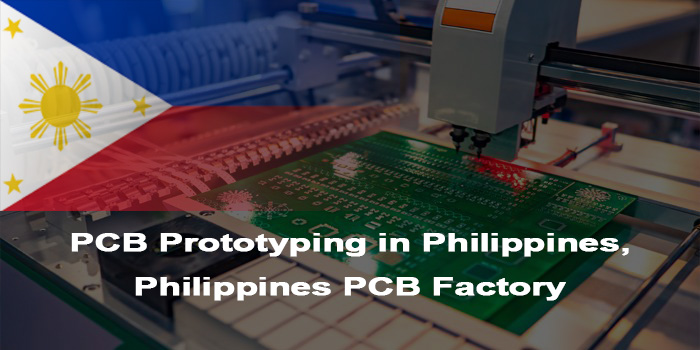
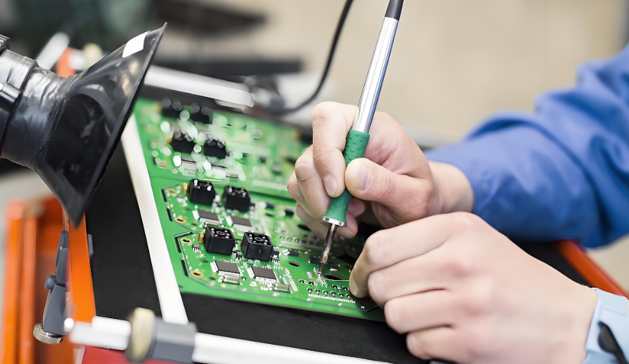
PCB prototype India has emerged as a reliable option for global electronics projects, fueled by policy support and advancing manufacturing capabilities. The country’s PCB prototype India services balance cost-effectiveness with adherence to international standards, catering to diverse sectors from automotive to consumer electronics. With growing local demand and global supply chain shifts, PCB prototyping in India is expanding its footprint, offering versatile solutions for small-batch and custom requirements.
Why Choose PCB Prototype India?
- Cost competitiveness: Labor costs are 20% lower than major Asian manufacturing hubs, supported by government PLI schemes offering up to 5% sales subsidies.
- Policy backing: “Make in India” initiative simplifies local sourcing and reduces import dependencies for PCB prototyping service in India.
- Skilled workforce: A growing pool of technically trained personnel proficient in modern fabrication techniques.
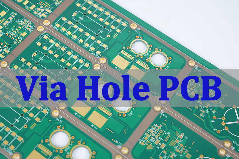
- Diverse capabilities: From single-layer boards to advanced HDI and rigid-flex prototypes, covering 90% of electronics applications.
- Strategic geography: Proximity to Middle East, Africa, and Europe reduces shipping time by 3-5 days compared to East Asian suppliers.
- Quality compliance: Increasing adoption of global certifications ensures alignment with international project requirements.
- Flexible production: Quick turnaround for small-batch prototypes, ideal for iterative testing and development cycles.
- Evolving infrastructure: Three major industrial clusters in Bangalore, Chennai, and Hyderabad enhance service accessibility.
Quality Standards for PCB Prototyping India
- IPC Standards: Compliance with IPC-A-600 (printed board suitability) and IPC-6012 (rigid PCB performance) as industry benchmarks.
- ISO Certifications: ISO 9001:2015 for quality management systems and ISO 13485 for medical device-specific prototypes.
- RoHS Conformity: Environmentally safe production with restricted use of hazardous substances.
- Automotive Grade: IATF 16949 certification for prototypes used in automotive electronics.
- AOI Testing: 100% automated optical inspection to detect soldering defects and trace errors.
- ESD-Safe Protocols: Dust-free and electrostatic discharge-controlled environments for precision fabrication.
Delivery Time for PCB Prototype India
| Prototype Type | Standard Lead Time | Express Lead Time | Volume Range |
| Single/Double-Layer PCB | 5-7 Days | 3-4 Days | 1-50 Units |
| Multilayer PCB (4-8 Layers) | 8-10 Days | 5-6 Days | 1-30 Units |
| HDI/Rigid-Flex PCB | 12-15 Days | 8-10 Days | 1-20 Units |
| Bus Bar PCB | 13-15 Days | 10-12 Days | 1-10 Units |
Top PCB Factory in India for Prototyping
| Company Name | Main Business | Core Advantages | Process Capabilities | Lead Time |
| EBest Circuit Co., Limited | Bus bar PCB, custom PCB prototyping & mass production | 18+ years experience, ISO/UL certified, one-stop service | 3-4 layer bus bar PCB, 1.0-3.0mm copper thickness, ENIG/gold plating | 13-15 days (standard), 10-12 days (express) |
| AT&S India Pvt. Ltd. | HDI, multilayer, microvia PCB prototypes & production | Austrian parentage, advanced facilities, automotive/aerospace certification | Up to 20-layer HDI, microvia technology, IATF 16949 compliant | 8-12 days (standard), 5-7 days (express) |
| PCB Power (CSIL) | Prototype PCB India, HDI, RF & multilayer PCBs | Online order platform, UL certified, express delivery | Single to 16-layer PCBs, RF PCB fabrication, AOI testing | 4-7 days (standard), 2-3 days (rush service) |
| Ascent Circuits Pvt. Ltd. | Rigid, flexible, rigid-flex PCB prototypes | Aerospace-grade quality, AS9100D certification, global exports | Rigid-flex PCBs, up to 12 layers, aerospace-grade materials | 10-14 days (standard), 7-9 days (express) |
| Shogini Techno Arts Pvt. Ltd. | LED, metal-core, single/multilayer PCB prototypes | Lighting industry expertise, IATF 16949, cost-effective | Metal-core PCBs, LED PCBs, up to 10-layer fabrication | 6-9 days (standard), 4-5 days (express) |
How to Choose the Right India PCB Factory for Prototyping?
A Selection Guide to PCB Factory in India for Prototyping:
- Verify certification coverage: Prioritize manufacturers with ISO 9001:2015 (quality management)、IATF 16949 (automotive) and ISO 13485 (medical) certifications, plus UL certification for substrate safety . These credentials ensure 99.5%+ yield and compliance with global market requirements for PCB prototype India.
- Assess process capabilities: Confirm layer range (4-16 layers for complex projects, up to 20 layers for HDI), minimum line width/space (0.1mm/0.1mm), and availability of AOI (surface defects) and X-ray (inner-layer/interconnect) testing to match prototype precision needs.
- Evaluate lead time reliability: Check the past 6-month on-time delivery rate (target ≥95%) and align express service timelines with the PCB prototyping in India standard (3-6 days for urgent orders), ensuring clear penalty clauses for delays.
- Review material sourcing: Ensure access to UL-certified substrates (FR-4 for general use, Rogers for RF applications) with 94V0 flame-retardant grade . Partner with factories having dual-supplier channels to keep import delay risk below 5%.
- Check after-sales support: Optimize for providers offering 24-hour DFM feedback with written reports, covering trace width, via placement and stackup optimization . Free iterative consultation for 1-2 design adjustments reduces rework costs.
- Compare cost structure: Request itemized quotes covering substrates, testing, packaging and shipping. Standard double-layer prototypes (100x100mm) start at $160/unit; clarify hidden charges (rush fees, design revisions) upfront to avoid budget overruns.
What Custom Options Does PCB Prototype in India Provide?
- Layer stackup customization: Tailored 2-20 layer configurations for specific signal integrity requirements.
- Surface finishing options: ENIG, immersion silver, gold plating, and lead-free solder finishes.
- Material customization: FR-4, polyimide, metal-core, and PTFE substrates for high-frequency/high-temperature applications.
- Bus bar PCB customization: 1.0-3.0mm copper thickness, bent configurations, and current capacity up to 300A.
- Design for Manufacturing (DFM) support: Feedback on trace width, clearance, and via placement to optimize yield.
- Panelization services: Custom panel designs for efficient assembly and reduced material waste.
- Specialized testing: X-ray inspection for BGA components, thermal testing for high-power prototypes.
Core Pain Points of PCB Prototyping Service India
- Raw Material Dependence: 70% of copper-clad laminates are imported, leading to price fluctuations and supply delays.
- Equipment Limitations: 90% of critical equipment (LDI, X-ray equipment) is imported, increasing maintenance costs and downtime risks.
- Insufficient Cleanroom Facilities: Most factories lack complete cleanroom standards, resulting in dust-induced defects in precision prototype products.
- Unstable Power Supply: Frequent voltage fluctuations disrupt production, affecting the consistency of prototype products even with backup systems.
- Shortage of Skilled Technicians: There is a 40% shortage of experienced technicians in advanced PCB manufacturing technology.
- Inconsistent Quality Control: Reliance on manual inspection leads to a 2-3% higher defect rate in small-batch prototype products.
- Inefficient Logistics: Domestic transportation delays result in 1-2 day longer delivery times for areas outside industrial clusters.
Future Trends of PCB Prototype India
- Policy-driven capacity expansion: Backed by a $46.4 billion electronic component manufacturing incentive plan , local PCB factory in India will accelerate HDI and flexible PCB R&D. Global firms like Samsung and Tata Electronics are already investing, boosting advanced prototype production capabilities.
- Supply chain localization deepening: India’s $6.26 billion PCB-focused subsidy projects will reduce 70% raw material import dependency. Local production of laminates and copper clad laminates will stabilize costs for PCB prototype India services.
- Green manufacturing mainstreaming: Stricter environmental regulations will drive 80% of factories to adopt low-waste processes. Wastewater treatment tech upgrades, supported by government grants, will cut operational costs while meeting global green standards.
- Domestic demand-driven specialization: With Xiaomi and Foxconn launching local PCB assembly plants , PCB prototyping service in India will focus on smartphone, automotive, and telecom sectors, forming niche competitive advantages against global players.
- Talent ecosystem construction: Public-private partnerships will address the 40% skilled labor gap. Training programs tailored for HDI fabrication and AOI testing will supply 34,000+ professionals annually , improving prototype quality consistency.
- Infrastructure integration across clusters: Government-backed projects will upgrade power grids and logistics in 8 states . Intra-country delivery delays will be cut by 1-2 days, aligning PCB prototyping in India with global delivery benchmarks.
- Digital transformation of production: To offset cost inflation, 60% of mid-to-large factories will adopt MES systems and AI-driven quality control. This reduces manual inspection defects by 2%+ and optimizes pricing for PCB prototype India services.
FAQs of PCB Prototype in India
Q1: Why do prototype PCBs from India have inconsistent solder mask application?
A1: This stems from manual process reliance and humidity fluctuations. The solution is to choose manufacturers with UV-curable solder mask and temperature/humidity-controlled SMT rooms, specifying 10-25µm mask thickness and 0.05-0.1mm expansion beyond pads.
Q2: How to avoid via plating defects in multilayer PCB prototypes from India?
A2: Defects occur due to incomplete plating and micro voids. The solution is to require tented vias, 1oz+ copper thickness, and X-ray inspection post-plating to ensure hole wall thickness ≥25µm.
Q3: Why do India PCB prototypes have thermal warping issues?
A3: Root cause is material selection mismatch and thermal expansion inconsistency. The solution is to specify substrates with appropriate Tg (≥170°C for industrial use) and match CTE values between layers, using polyimide for high-temperature applications.
Q4: How to ensure traceability for prototype PCBs from India?
A4: Traceability gaps exist in mid-tier facilities. The solution is to partner with manufacturers using MES systems and board-level traceability, requiring batch-specific documentation for raw materials and testing.
Q5: What causes signal integrity issues in RF PCB prototypes from India?
A5: Issues arise from incorrect material selection and poor trace design. The solution is to use Rogers/PTFE substrates for RF prototypes, ensure 50Ω impedance control, and request signal integrity simulation before fabrication.