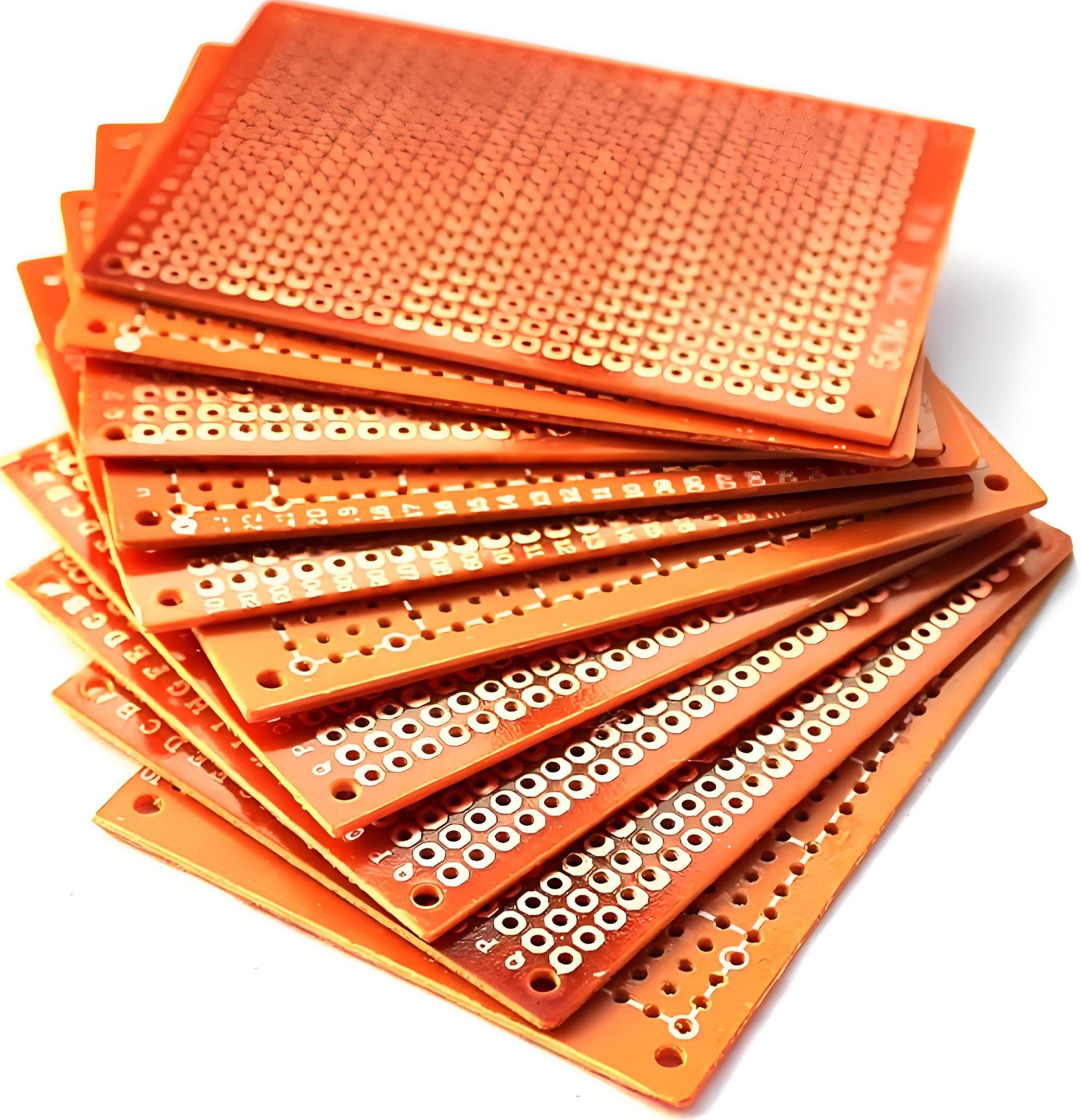
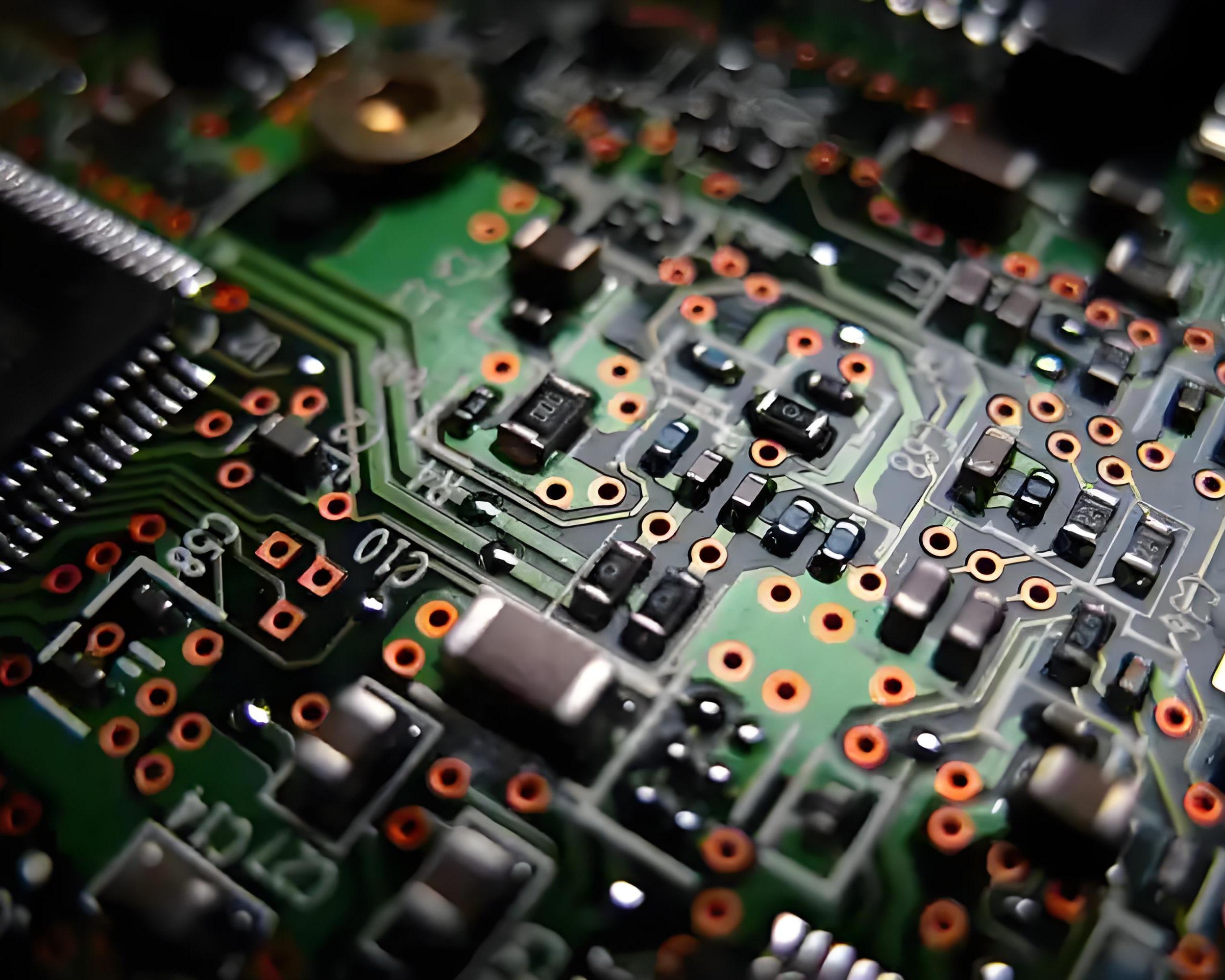
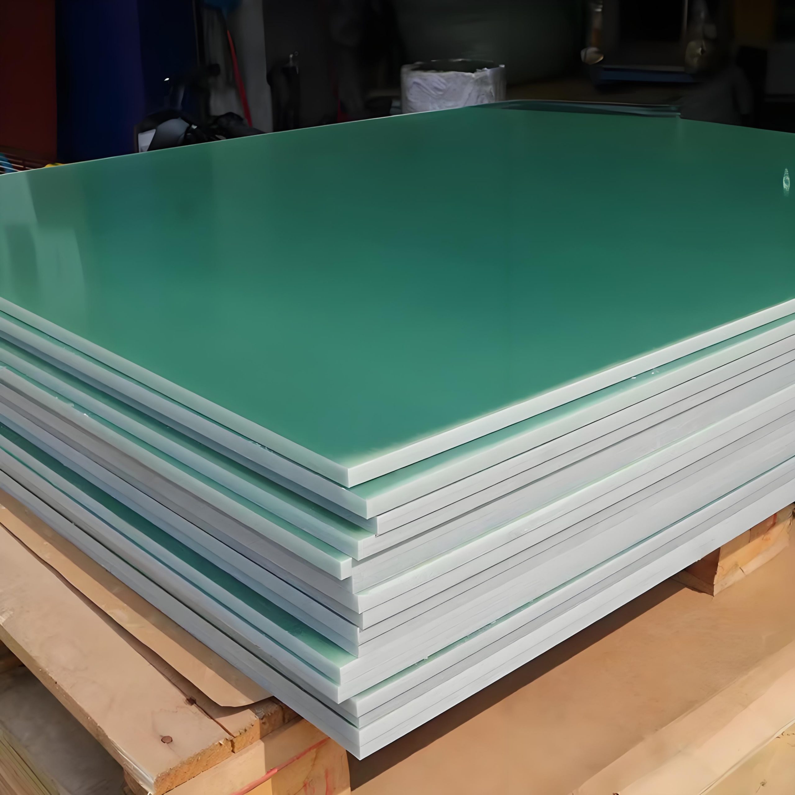
What is the density of FR4?The density of FR4 generally ranges from 1.9g/cm³ to 2.2g/cm³. FR4 is a glass fiber epoxy laminate commonly used in PCB manufacturing. It has high mechanical strength, good heat resistance and excellent electrical properties, so it is widely used in the manufacture of electronic products.
How much does FR4 weigh?
The weight of FR4 varies depending on the thickness and size of the board. It is an epoxy glass fiber cloth laminate, and its weight mainly depends on its volume and density.
The formula for calculating weight (W) is W = ρ*V, where (V) is volume and (ρ) is density.
Therefore, the weight of FR4 depends on its volume (determined by length, width, and thickness) and density. After knowing the specific size and density, the weight can be accurately calculated.
What is the raw material of FR4?
The raw materials of FR4 mainly include glass fiber and epoxy resin.
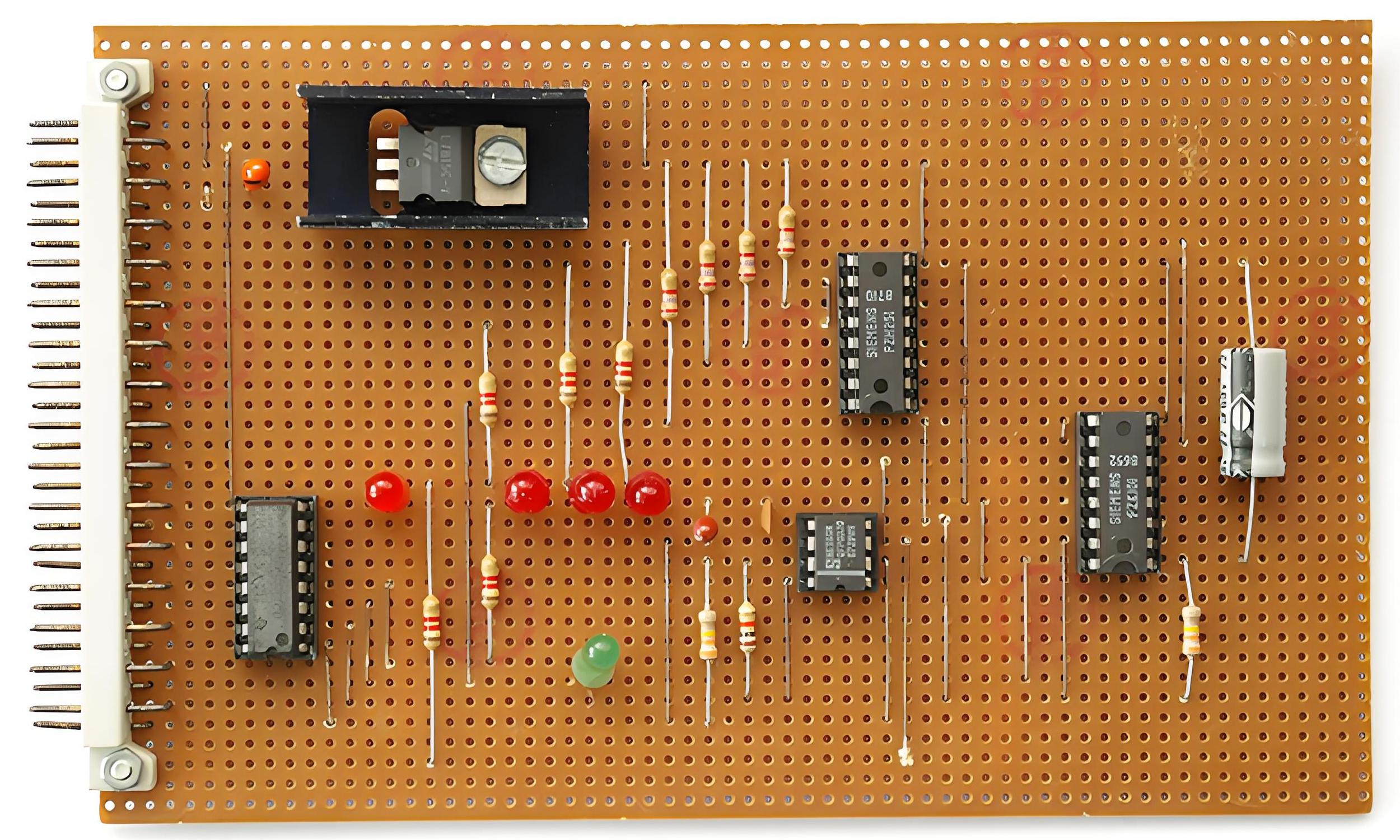
FR4 is a composite material made of glass fiber cloth impregnated with epoxy resin and then formed under high temperature and high pressure.
Specifically, FR4 is an epoxy board with a flame retardant grade of 4. Its raw materials include epoxy resin, an organic polymer compound, and glass fiber. This material has excellent insulation, mechanical strength and heat resistance, and is widely used in the electronics industry.
How thick is FR4 PCB material?
The common thickness range of FR4 PCB material is 0.2mm to 3.2mm, of which the most common thickness is 1.6mm.
Specific common thicknesses include 0.3mm, 0.4mm, 0.5mm, 0.6mm, 0.8mm, 1.0mm, 1.2mm, 1.5mm, 1.6mm, 1.8mm, 2.0mm, etc.
In addition, the common thickness of FR4 rigid board is 0.8-3.2mm, while the common thickness of thin board is less than 0.78mm.
What are the properties of FR4 material?
The main properties of FR4 material include flame retardancy, mechanical properties, electrical properties, heat resistance, chemical resistance and environmental protection.
- Flame retardancy: The “FR” in FR4 material stands for “Flame-Retardant”, which means flame retardant. It contains special chemicals that can slow down the spread of fire when a fire occurs and protect electronic equipment from damage.
- Mechanical properties: FR4 has high strength and stiffness, with tensile strength and compressive strength of up to 65,000 psi and 38,000 psi respectively, which makes it perform well when subjected to mechanical stress.
- Electrical properties: FR4 maintains good insulation properties in both dry and humid environments. Its dielectric constant is 4.2-4.7, and the dielectric constant changes with temperature, but it does not change much in the temperature range of 0-70 degrees.
- Heat resistance: The heat resistance of FR4 is represented by the glass transition temperature (Tg), which is usually 130°C, 140°C, 150°C or 170°C. It will not deform or melt when used at 160°C, ensuring the stability and service life of the material.
- Chemical resistance: FR4 has good chemical resistance and can resist erosion in corrosive environments such as acids and alkalis.
- Environmental protection: With the increasing awareness of environmental protection, the environmental protection characteristics of FR4 are also valued. Its flame retardant rating reaches 94V-0, and it produces almost no harmful gases when burning, which is more friendly to the environment and human health.
What does the 4 stand for in FR4?
The “4” in FR4 represents its material grade and specific chemical composition.
FR4 is a flame-retardant glass fiber reinforced epoxy laminate, where “FR” stands for “Flame Retardant” and the number “4” indicates the specific grade of this material.
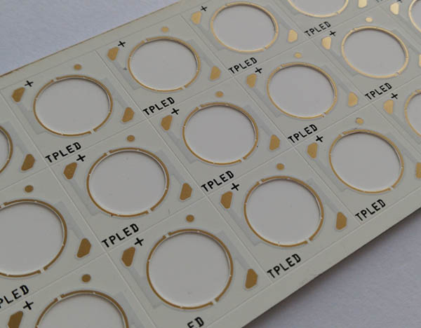
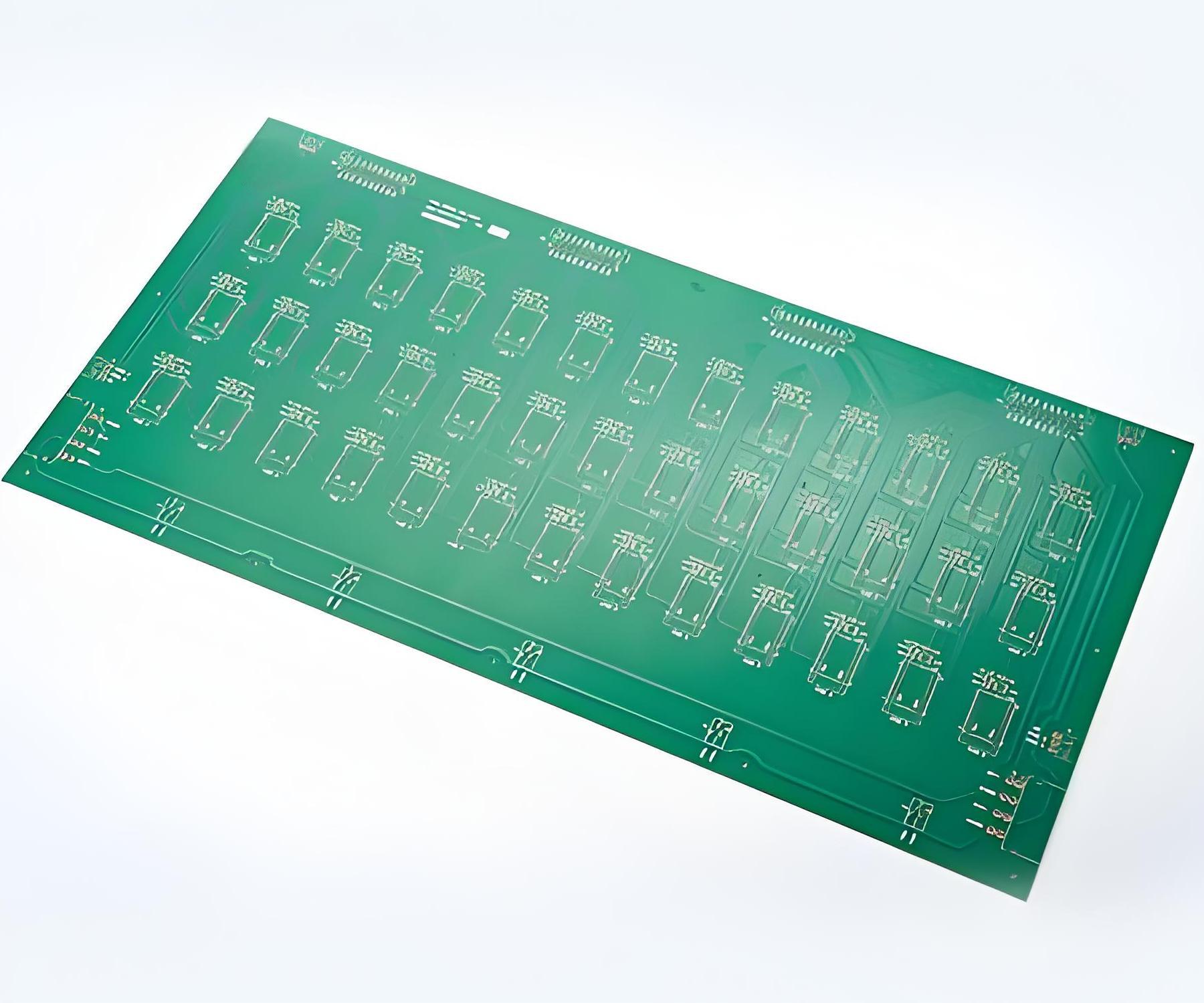
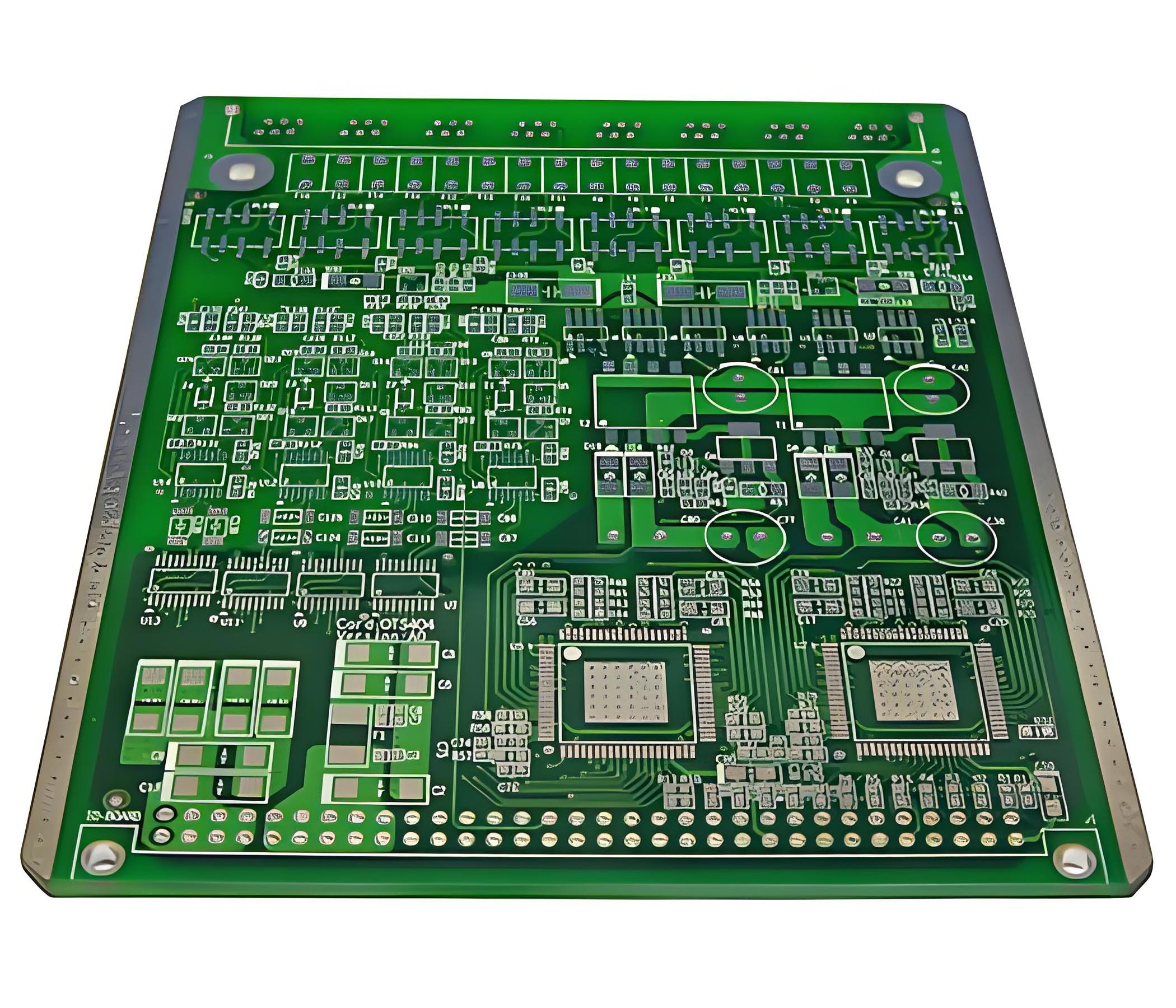
Specifically, FR4 is a double-sided copper-clad PCB board made of epoxy resin and glass fiber cloth, which has excellent mechanical strength, electrical insulation, heat resistance and flame retardancy.
FR4 has a flame retardant rating of UL94 V-0, which means that it can quickly self-extinguish when burning, greatly improving the safety of electronic products. In addition, FR4 also has excellent mechanical properties, can withstand high temperatures and physical stress, and has good electrical insulation and low moisture absorption, making it suitable for a variety of electronic devices.
What is high Tg FR4 material?
High Tg FR4 material is a special printed circuit board material with a high glass transition temperature (Tg), usually above 170°C. High Tg FR4 material can maintain stable performance and shape in high temperature environments, so it is widely used in electronic devices that need to withstand high temperature and high stress environments.
Advantages and application areas of high Tg FR4 material
- High temperature resistance: High Tg FR4 material can maintain the stability of shape and performance in high temperature environments, and is suitable for high temperature electronic equipment, automotive electronics, aerospace and communication equipment and other fields.
- Good electrical properties: Even at high temperatures, high Tg FR4 material can still maintain good electrical properties to ensure the stable operation of the circuit.
- Stable mechanical properties: High Tg FR4 material has a low coefficient of thermal expansion and can maintain its shape at high temperatures, avoiding curling and deformation.
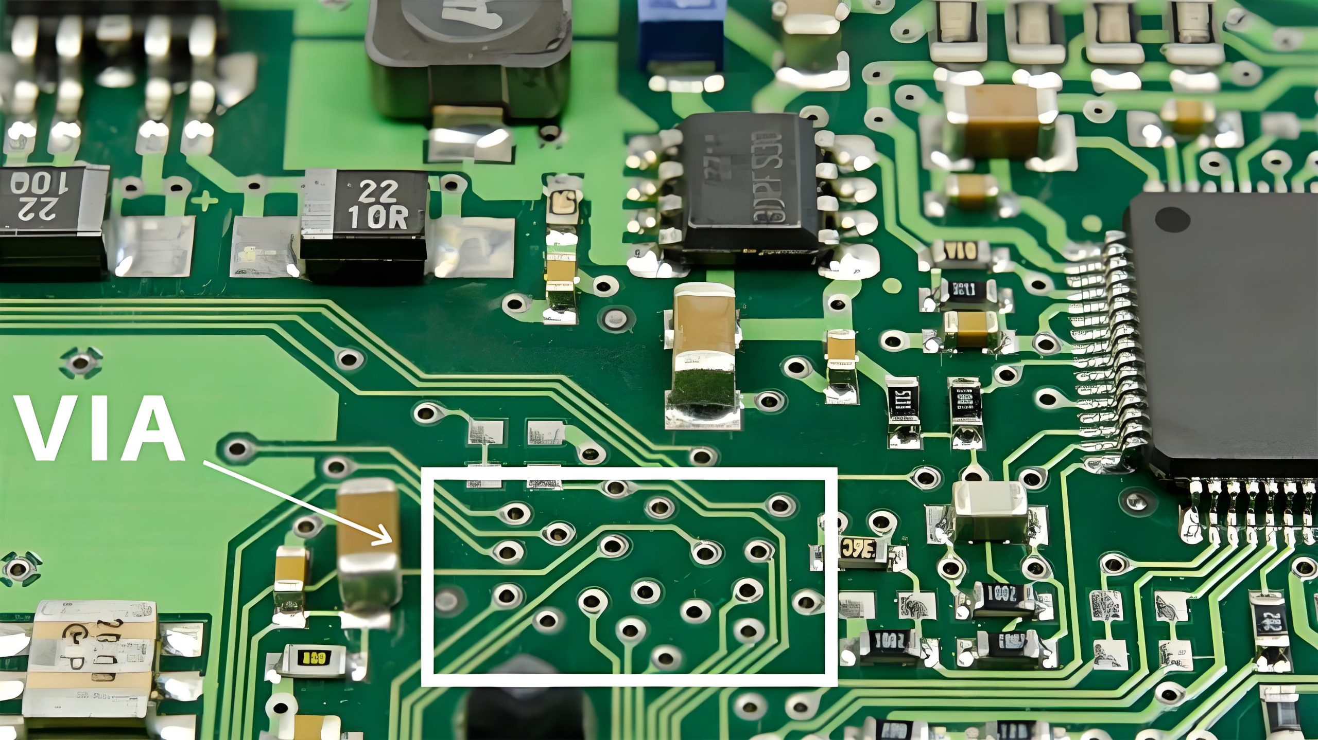
Why is FR4 used in PCB?
There are several reasons why FR4 material is widely used in PCB:
- Good insulation: In a circuit, it is crucial to prevent current from flowing in unintended paths. FR4 material is an excellent insulator that can effectively isolate different conductive lines, avoid short circuits, and ensure the normal operation of the circuit.
- Stable dielectric constant: The dielectric constant of FR4 is relatively stable, which is very critical for the transmission of high-frequency signals. A stable dielectric constant can reduce signal delays and distortion during transmission and ensure signal integrity.
- Good dimensional stability: FR4 has a low coefficient of thermal expansion, and its dimensional changes are small when the temperature changes, which can keep the PCB size relatively stable and ensure that the connection between electronic components will not loosen or be damaged due to thermal expansion and contraction.
- Chemical corrosion resistance: FR4 material has good tolerance to many common chemicals and can resist corrosion from chemicals such as acids, alkalis, and salts, thereby protecting the internal structure and electrical performance of the PCB from damage.
- Good moisture resistance: Moisture is one of the biggest enemies of electronic equipment, which may cause circuit short circuits, component damage and other problems. FR4 material has a certain moisture resistance, which can prevent the intrusion of moisture and reduce the risk of PCB failure in a humid environment.
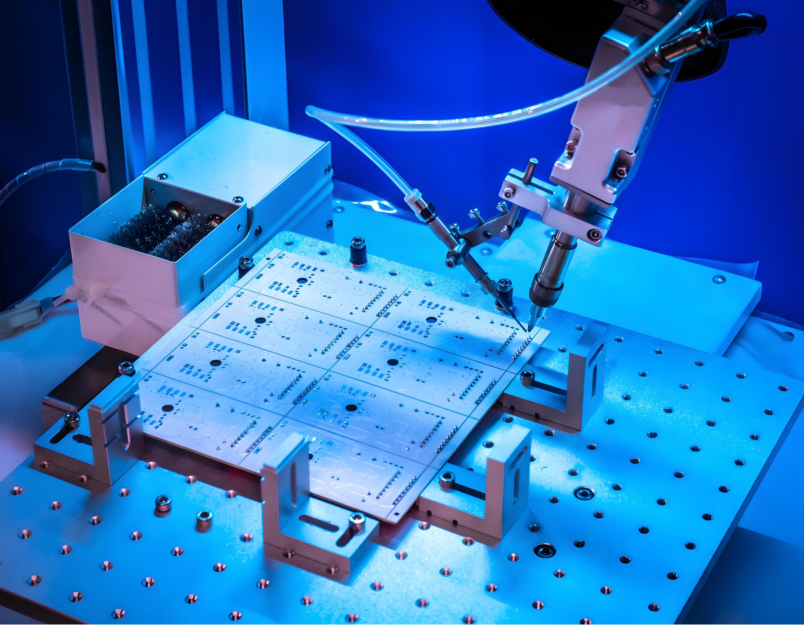
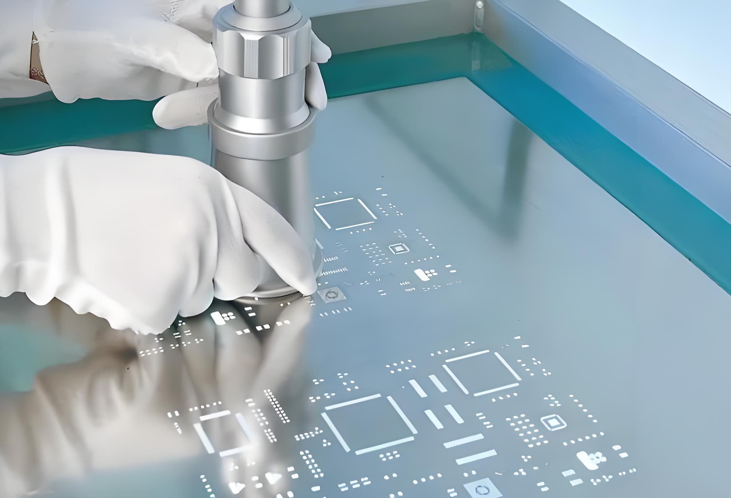
- Easy to process and shape: FR4 material can be easily made into PCBs of various shapes and sizes through a variety of processing techniques. It is suitable for conventional PCB manufacturing processes such as drilling, cutting, and etching, and can ensure high processing accuracy and quality.
- Relatively low cost: Compared with some high-end special materials, the cost of FR4 material is more reasonable. While meeting the performance requirements of most electronic devices for PCBs, it can effectively control production costs.
In short, the density of FR4 is determined by raw materials and processes. This density has a significant impact on the mechanical properties, electrical properties, and processing technology of the PCB. In production, rigorous measurement and quality control are used to ensure that the density meets the standards. As a professional PCB manufacturer, BEST Technology is well aware of the key role of FR4 density. From material selection to processing, it strictly follows the standards and relies on exquisite craftsmanship to create PCBs with excellent performance for customers to meet diverse electronic needs.