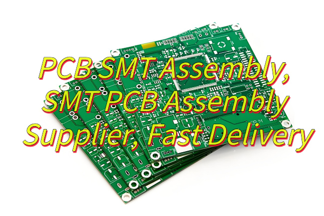
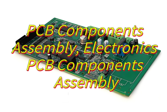
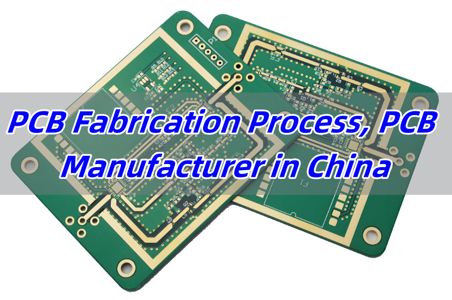
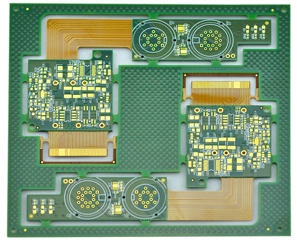
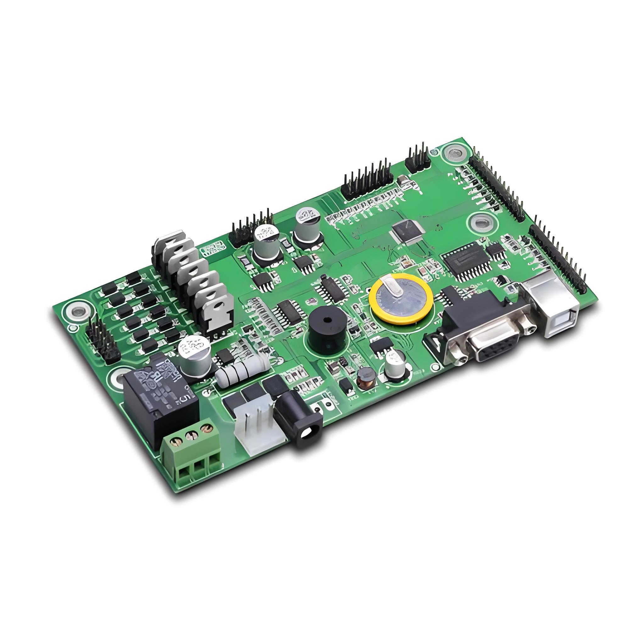
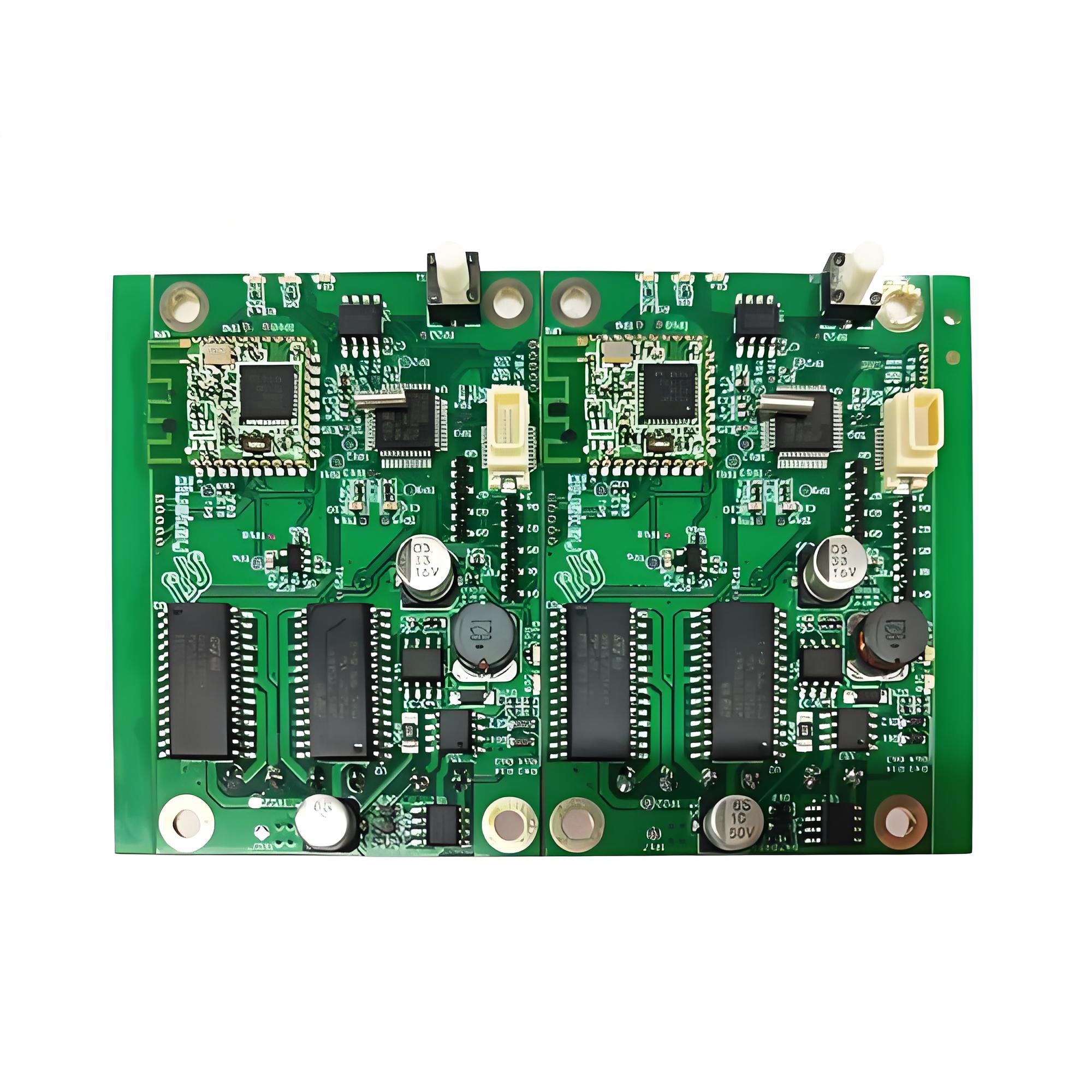
Assembling and testing electronic components on a small PCB is a critical process in electronics design and production. As electronic devices continue to shrink, the need for high-quality small PCBs grows rapidly. These boards are used in wearables, portable medical equipment, compact consumer gadgets, and more.
In this detailed guide, we’ll cover the most frequently asked questions about small PCB assembly and testing. You’ll learn the importance of miniaturized boards, how to handle the assembly process, and the various methods for reliable testing.
Why Are Small PCBs Important?
Small PCBs play a major role in modern electronics where compact size and lightweight form factors are essential. Whether it’s a smartwatch, fitness tracker, or smart home sensor, space is always limited. Miniaturized PCBs make it possible to fit complex electronic functions into these tiny enclosures.
But it’s not just about saving space. Small PCBs often improve signal integrity by reducing the length of signal paths. This is especially helpful in high-speed applications. Moreover, they reduce parasitic capacitance and inductance, which enhances performance in analog and RF circuits.
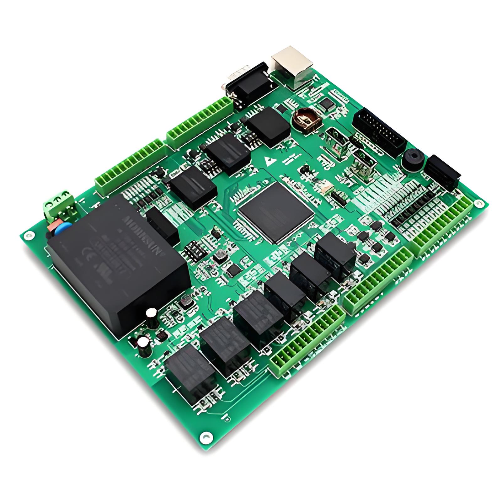
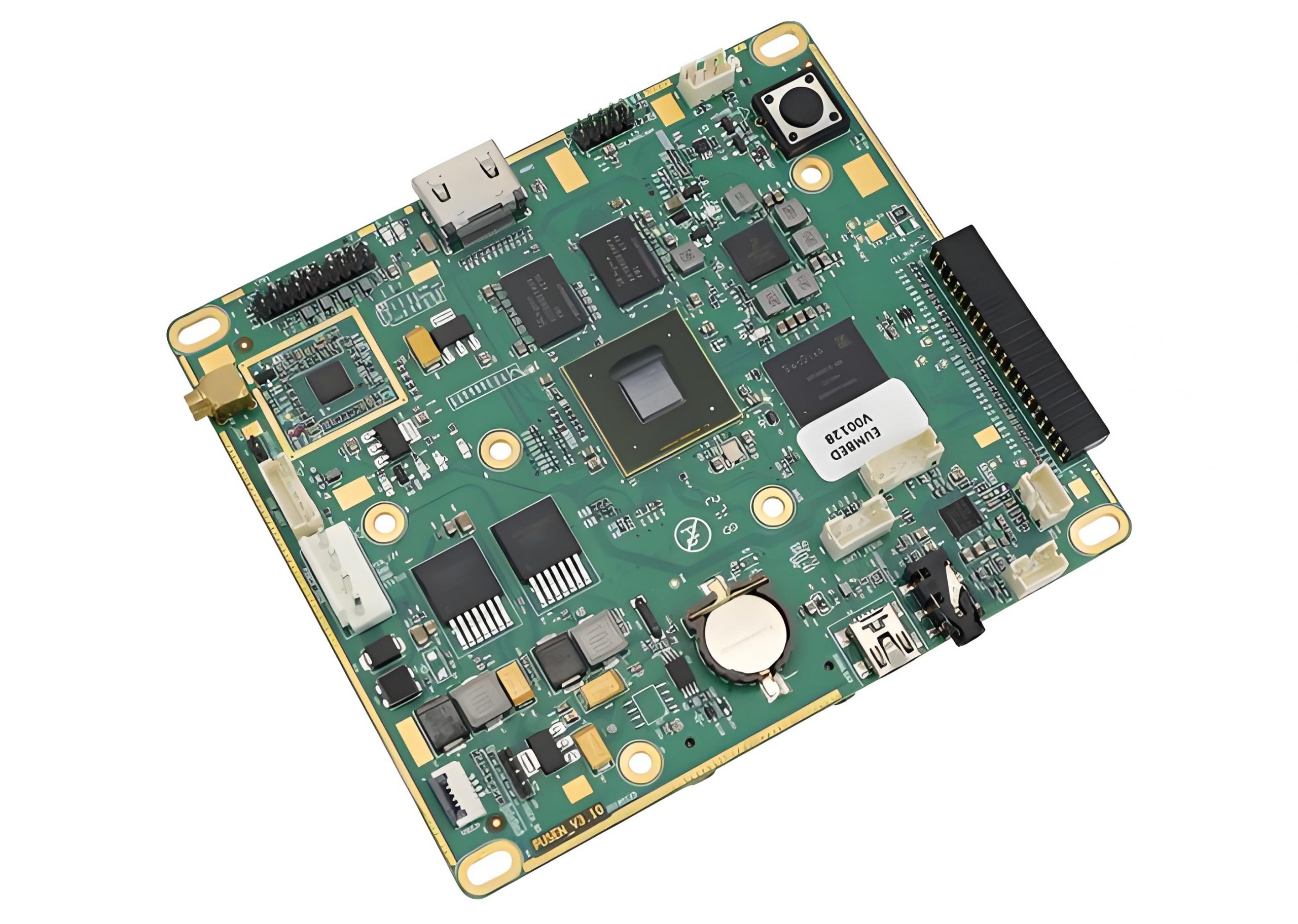
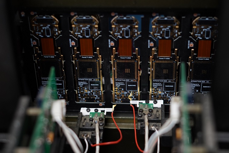
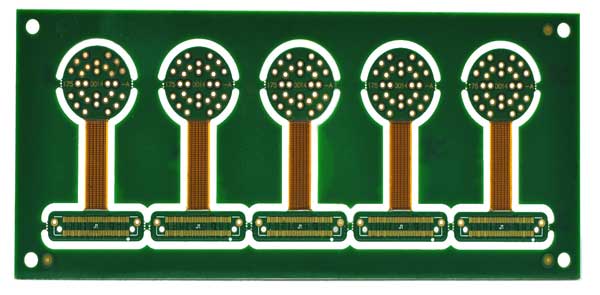
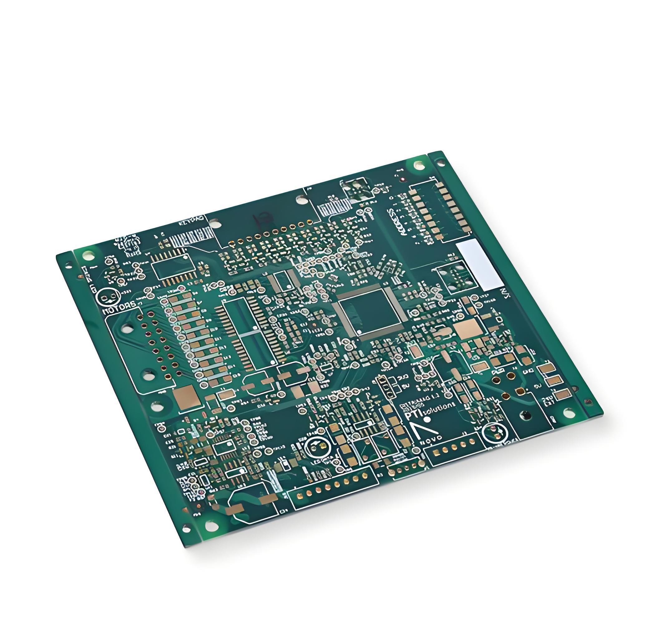
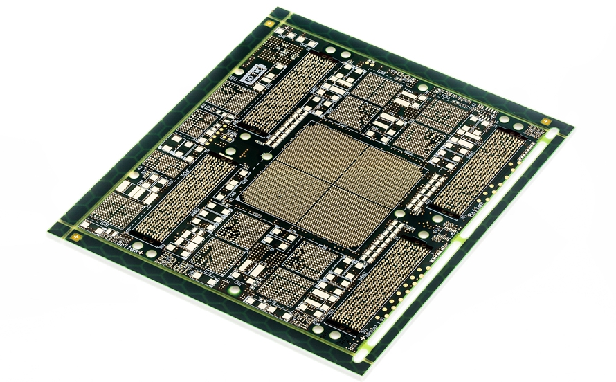
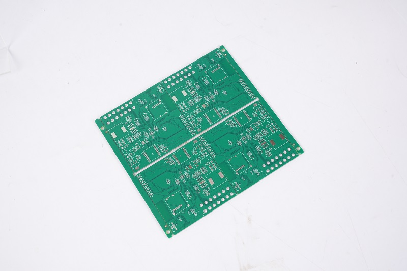
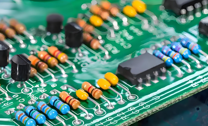
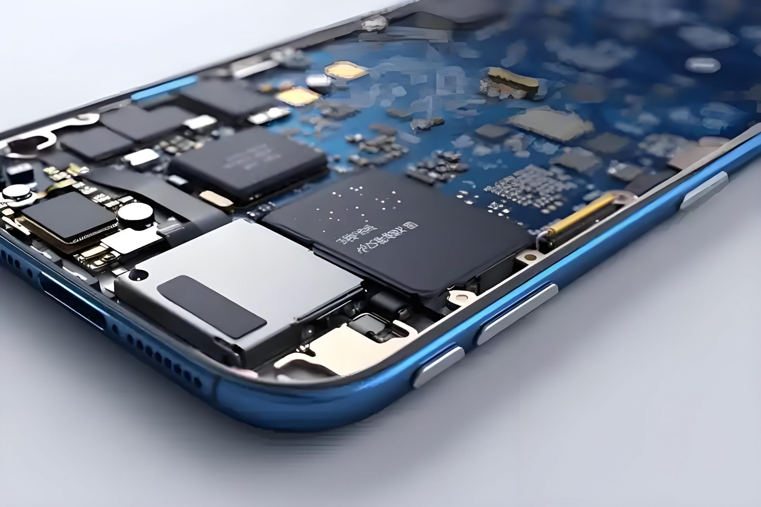
Additionally, small PCBs contribute to overall system efficiency. They use fewer materials, require less power, and simplify thermal management when designed properly. With all these advantages, it’s no surprise that assembling and testing small PCBs has become a specialized field in electronics manufacturing. Here is the main motherboard used in mobile phone:
How Do You Test a Small Circuit Board?
Testing a small circuit board involves several steps, each tailored to ensure functionality and identify defects before the board is installed in a final product. The key challenge lies in the limited real estate, which makes access and probing more difficult. Despite this, the following steps are commonly used:
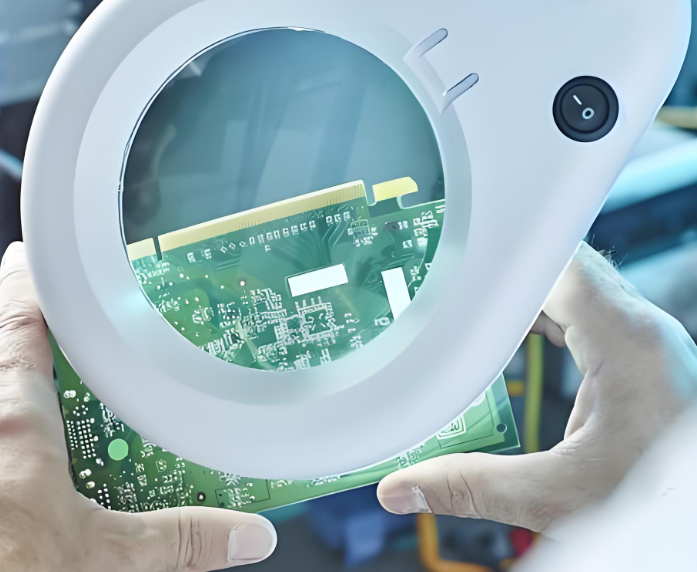
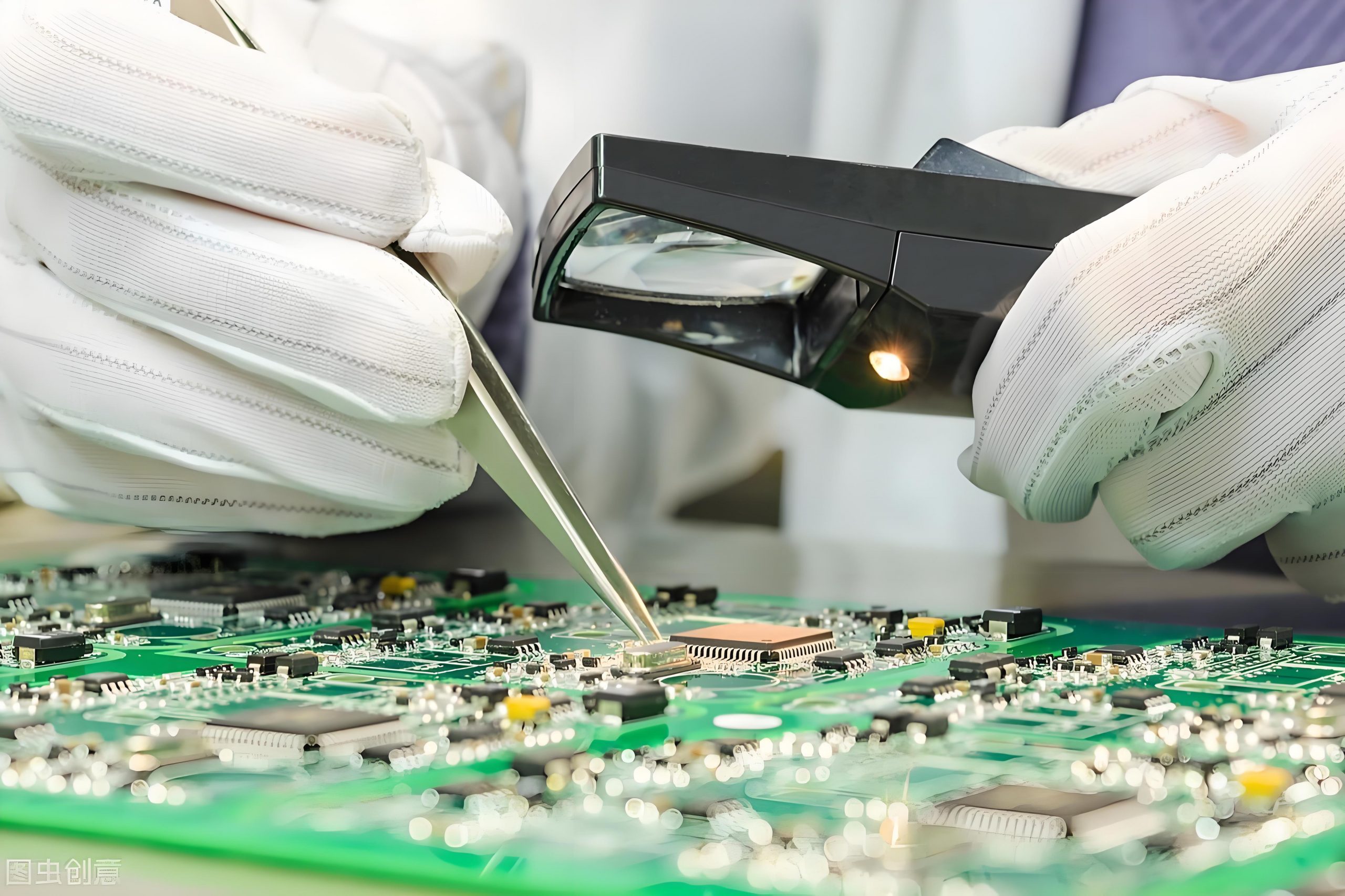
1. Visual Inspection
Begin with a close-up inspection, using magnification tools or a microscope. You’re looking for:
- Solder bridges
- Tombstoned components
- Incorrect polarities
- Cracked or missing parts
2. Continuity and Resistance Checks
Use a multimeter to test for continuity along copper traces. Any open line could indicate a manufacturing error, such as an incomplete etch or a broken solder joint.
3. Power-On Testing
Once you’ve confirmed no shorts, apply power using a bench supply. Use a limited current setting to avoid damaging the board if something goes wrong. Confirm that voltage rails (e.g., 3.3V, 5V) match design specifications.
4. Functional Component Checks
Activate the board’s subsystems one at a time. For example, if there’s an LED or sensor, trigger them with known inputs and check the response.
5. Oscilloscope or Logic Analyzer
In digital systems, probe clock signals, data buses, and communication lines (like I2C, SPI, or UART). On analog boards, check waveform quality and frequency.
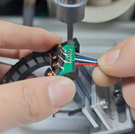
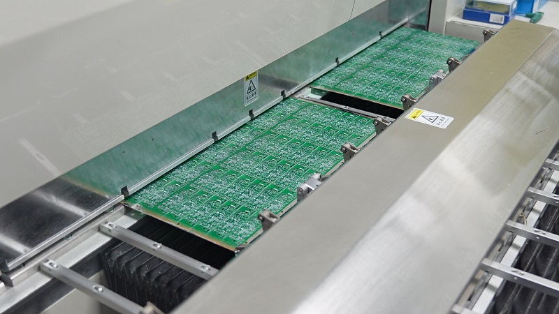
How to Assemble Electronic Components on a Small PCB?
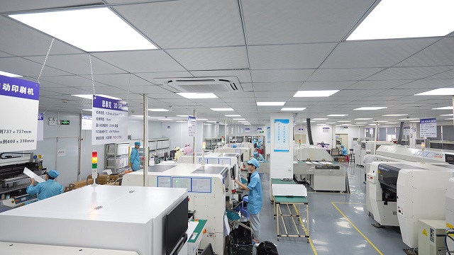
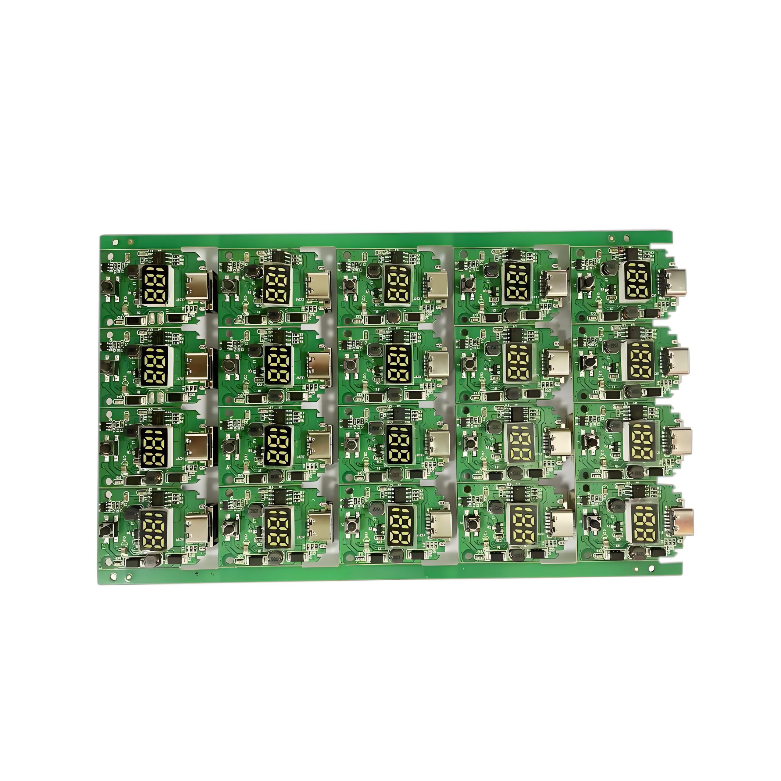
Assembling electronic components on a small PCB involves precise coordination between manual work and machine automation. Small PCBs typically use surface-mount technology (SMT), though some through-hole components may still be involved. You can follow below steps to assemble components on your PCB.
1. Workspace Preparation
Ensure the working environment is ESD-safe. Use grounded wrist straps, antistatic mats, and proper lighting. A clean environment reduces contamination risks and improves soldering quality.
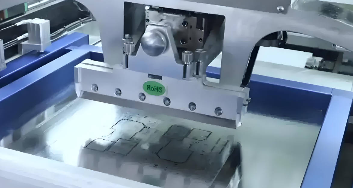
2. Stencil and Solder Paste Application
Use a laser-cut stencil to apply solder paste accurately on each pad. This ensures that components receive just the right amount of solder, which is critical for small pads.
3. Pick-and-Place Process
Surface-mount components are placed using tweezers (manual) or a pick-and-place machine (automated). For very small boards, the manual method is common in low-volume runs.
4. Reflow Soldering
After placement, the PCB passes through a reflow oven where the solder paste melts and solidifies, bonding the components securely. The reflow temperature profile must be carefully controlled.
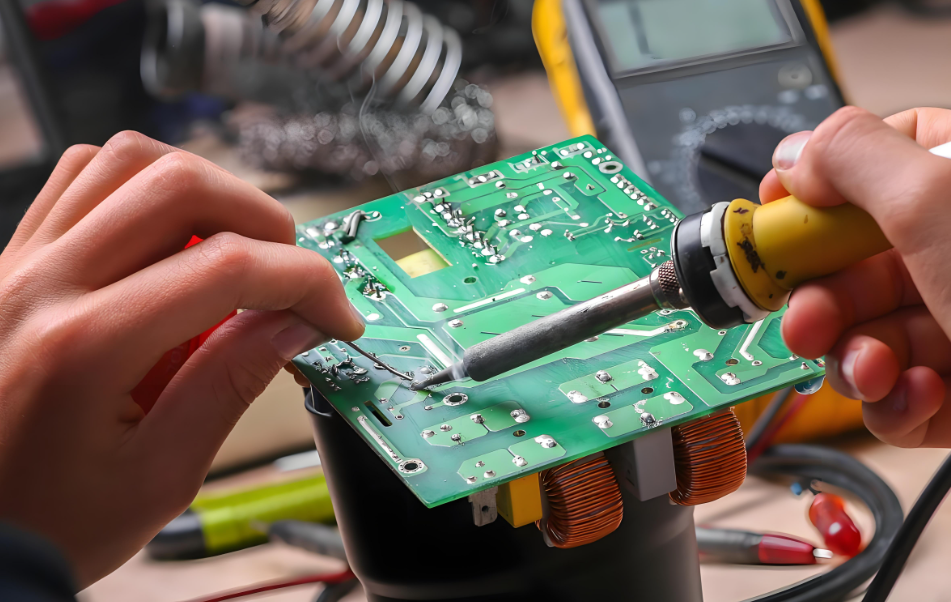
5. Inspection and Touch-Up
Once soldered, the board is inspected under magnification. Cold joints, solder bridges, or shifted components are corrected using a fine-tip soldering iron or hot air tool.
6. Through-Hole Soldering (if applicable)
If your design uses connectors or switches, those are added next. Insert them into the board and hand-solder from the bottom side.
7. Final Cleaning
Any flux residue left after soldering should be cleaned with isopropyl alcohol or a PCB cleaning solution. This prevents corrosion and improves reliability.
How to Test Components on a PCB?
Once the PCB is assembled, testing individual components confirms they are working and properly connected. You don’t always have to remove parts from the board—many can be tested in-circuit.
Testing Common Components:
- Resistors: Measure resistance values across the component with a multimeter.
- Capacitors: Use a capacitance meter or LCR meter. Electrolytics should be tested for leakage or swelling.
- Diodes/LEDs: Use diode mode to check forward voltage. LEDs will glow slightly if working.
- Transistors: Use a component tester or check base-emitter junctions with a multimeter.
- Integrated Circuits: For complex ICs, test power and ground pins, and validate input/output behavior using a scope.
Note: Some components may give inaccurate readings in-circuit due to parallel paths. If readings are questionable, desolder one leg and test again.
What Are the 7 Types of PCB Testing Methods?
1. Visual Inspection
Used in early quality checks. Technicians or AOI systems look for visible defects like misalignment, poor soldering, and missing parts.
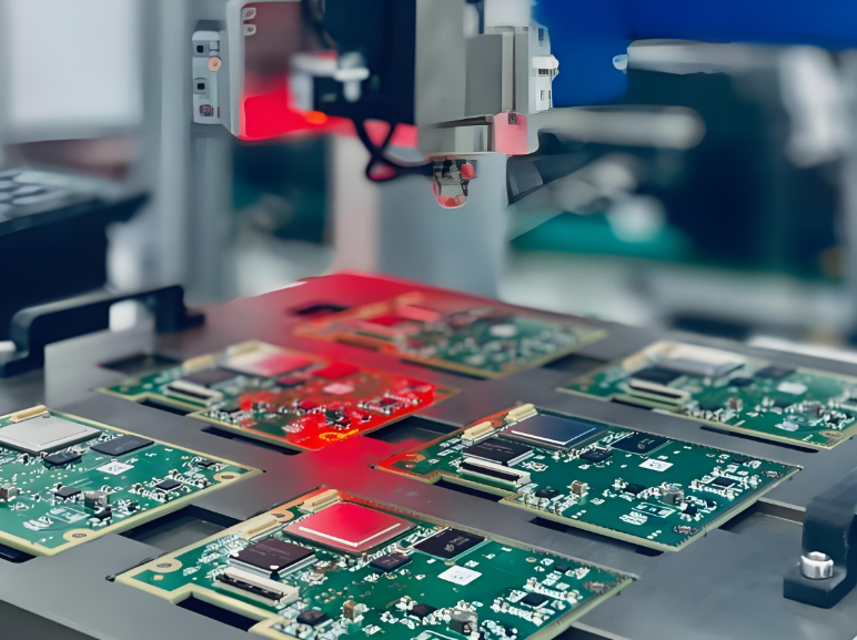
2. In-Circuit Testing (ICT)
A bed-of-nails fixture probes test points across the PCB. It checks resistance, capacitance, and signal paths individually. Best for high-volume manufacturing.
3. Flying Probe Test
A non-fixture alternative to ICT. Probes move automatically to check test points. Suitable for prototypes and small production runs.
4. Functional Testing
Simulates real-world operation. Inputs are applied, and outputs are measured to ensure the board works as expected.
5. Boundary Scan Testing
Used for densely packed ICs like BGAs. Tests internal connections and inter-chip communication using a special interface (JTAG).
6. Burn-In Testing
Applies power for extended periods under stress conditions. Helps detect early-life failures or unstable components.
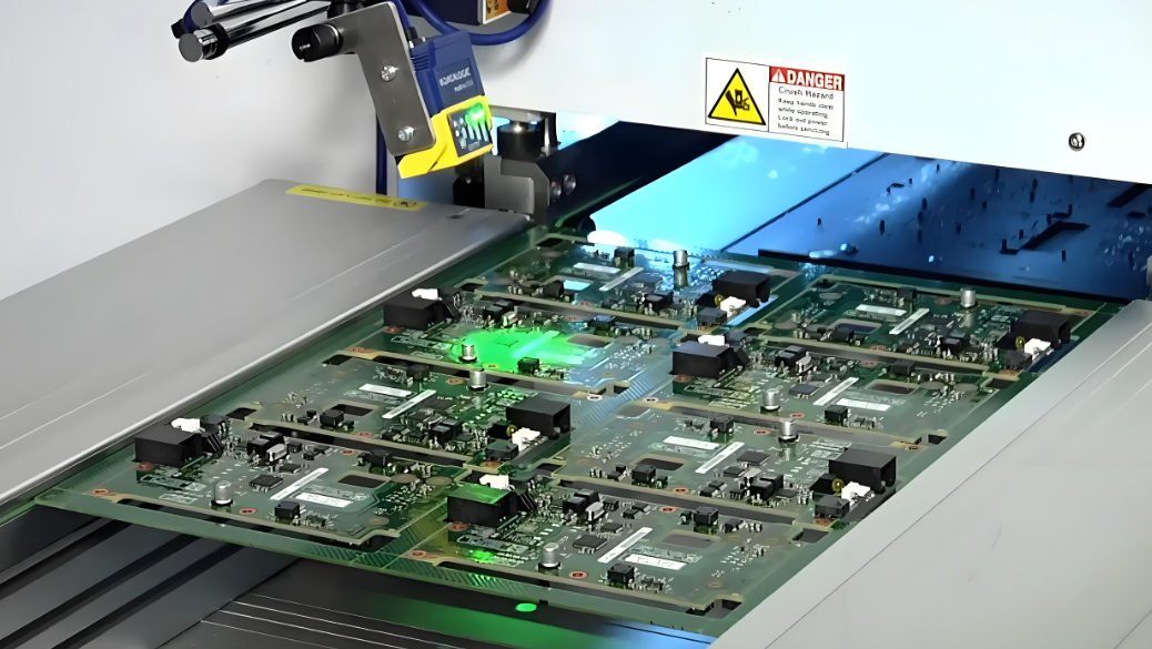
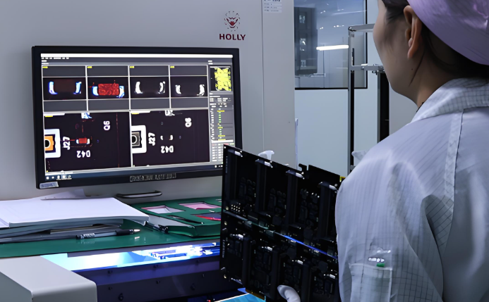
7. Automated Optical Inspection (AOI)
High-speed cameras scan the board for defects after assembly. AOI systems compare images to a golden board and flag mismatches.
How to Find a Bad Component on a Circuit Board?
Finding a faulty component on a small PCB is part detective work, part experience. Here’s a logical way to do it:
1. Visual Clues
Burned areas, cracked packages, or leaked electrolytes are red flags. Look for parts that appear physically damaged or discolored.
2. Voltage Checks
Measure voltages across IC pins and power rails. An unexpected drop may point to a shorted capacitor or faulty regulator.
3. Thermal Inspection
Use a thermal camera or just touch carefully. A component heating abnormally might be shorted internally.
4. Signal Tracing
Use a scope or logic analyzer to trace where signals stop behaving correctly.
5. Component Testing
Compare suspect part readings to known-good values. Swap out parts if needed to confirm suspicion.
How Do You Identify Electronic Components on a Circuit Board?
Understanding how to identify components on a PCB helps in repairs, testing, and reverse engineering. Here are some methods that can help you to identify the components:
- Look at the Silkscreen: Reference designators like R5 (resistor), C3 (capacitor), U2 (IC) help locate parts quickly.
- Check the Values: Printed numbers often reveal resistance, capacitance, or voltage ratings.
- Use Datasheets: For ICs and transistors, part numbers can be searched online for specs and pinouts.
- Refer to Schematics: The design files give a complete map of how everything connects.
- Use a Component Tester: These handheld tools can identify unknown parts and help verify pin functions.
About EBest Circuit (Best Technology)
EBest Circuit (Best Technology) is a leading PCB manufacturer and assembler in China, offering full-service solutions for small PCB fabrication, SMT assembly, and functional testing. We provide:
- PCB prototyping and mass production
- Turnkey assembly with DFM support
- Functional and in-circuit testing
- Full traceability via MES system
- Fast quotes and professional engineering advice
If you need a reliable partner for assembling and testing PCBs, reach out to EBest Circuit (Best Technology) today.
Common FAQs about PCB
1. Can I assemble a small PCB at home?
Yes, with the right tools like a soldering iron, tweezers, magnifier, and steady hands, you can assemble small PCBs manually.
2. What’s the safest way to test a new PCB?
Start with a multimeter check for shorts, then use a bench power supply with current limiting to test under controlled conditions.
3. Can I use AOI on low-volume runs?
Manual inspection is more cost-effective for low volumes, but desktop AOI systems are now affordable for small labs.
4. How do I avoid soldering errors on small PCBs?
Use a stencil for even paste application, magnification to inspect, and reflow ovens with the right temperature profile.
5. Do I need ICT or flying probe testing?
ICT is better for large batches. Flying probe is ideal for prototyping or small batch production without custom fixtures.