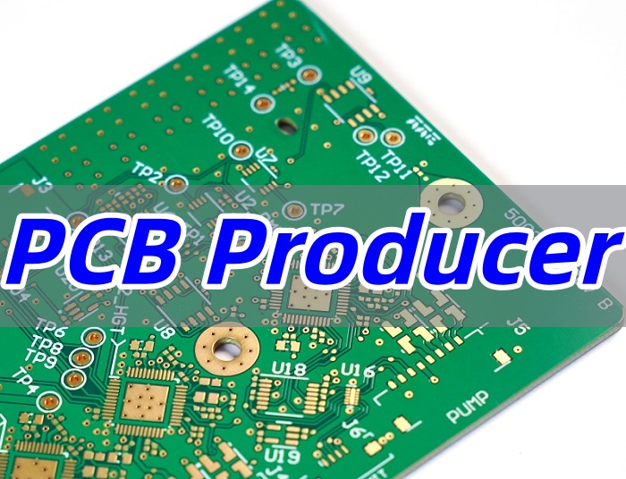
Prototyping & small-batch PCBs are the essential, iterative foundation of any successful electronic product, allowing designers to test, validate, and refine their concepts before committing to mass production. This comprehensive guide will explore everything you need to know about these critical stages, from key definitions and technical comparisons to selecting the right manufacturing partner for your project.
Navigating the world of PCB fabrication, especially during the critical early stages, presents several common challenges. Are you struggling with:
- Unexpected costs that derail your project’s prototyping budget?
- Agonizingly long lead times that slow down your development cycle?
- Inconsistent quality and unclear communication from the manufacturer?
- Technical limitations when your design requires advanced capabilities?
- Difficulty transitioning smoothly from a few prototypes to a small-batch run?
These pain points are precisely why a strategic approach to prototyping & small-batch PCBs is vital. Here’s how a reliable partner addresses these core issues:
- Transparent, up-front pricing with no hidden fees to protect your budget.
- Guaranteed rapid turnaround times to keep your project on schedule.
- Rigorous quality control standards and dedicated engineering support.
- Access to advanced technologies and materials to bring complex designs to life.
- Seamless scaling from a single prototyping pcb board to hundreds of units with consistent quality.
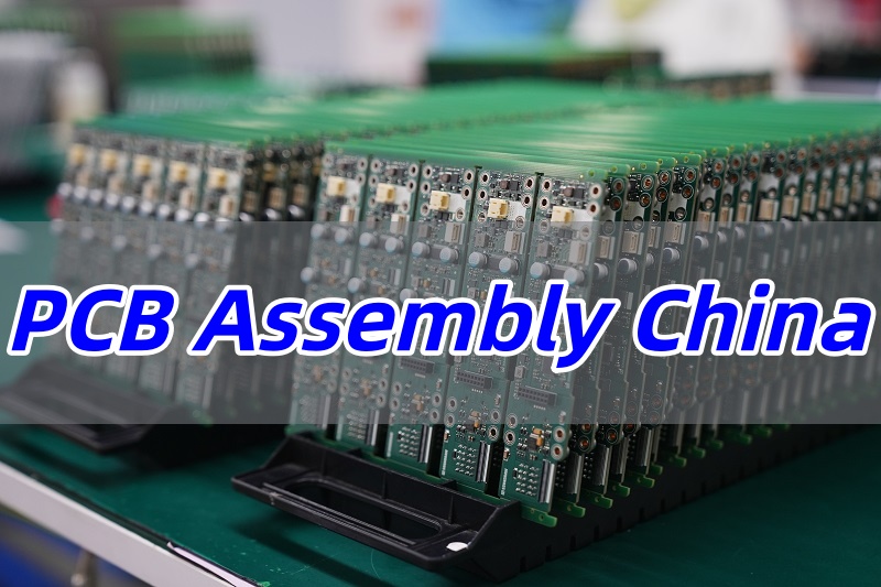
At BEST Technology, we specialize in overcoming these challenges. As a professional PCB manufacturer with extensive expertise in both standard and advanced materials, we are committed to providing superb quality prototyping & small-batch PCBs that accelerate your innovation. Contact us at sales@bestpcbs.com to discuss your specific requirements.
What Are Prototyping & Small-Batch PCBs?
In electronics development, prototyping & small-batch PCBs represent the early stages of circuit fabrication, designed for functional testing, design verification, and short-run production. These boards help engineers uncover design issues, validate performance, and collect feedback before scaling to mass manufacturing.
Definition and Purpose: A prototype PCB is the first tangible form of a circuit design, built to verify electrical and mechanical accuracy. Meanwhile, small-batch PCB production usually ranges from a few dozen to several hundred units—ideal for beta testing, pilot runs, or limited-edition applications. Together, they bridge the gap between concept and commercial readiness.
Application Scenarios: Such PCBs are essential across R&D departments, university projects, startup innovations, and retrofitting of legacy equipment. Today, the ability to order a PCB prototype online has simplified access for both professionals and hobbyists, making rapid innovation easier than ever.
Critical Importance: Skipping proper prototyping can result in costly design errors and production setbacks. Investing time in this stage ensures the final product is electrically reliable, structurally sound, and fully manufacturable at scale.
In essence, prototyping & small-batch PCBs are more than just preliminary steps—they are strategic safeguards that determine the success, reliability, and speed of your product’s market entry.
What are the Features between PCB Prototype USA and PCB Prototype China?
Selecting where to manufacture your PCB prototypes involves balancing cost, speed, and technical needs. Below is a concise comparison between PCB prototype USA and PCB prototype China to help guide your decision.
Cost Efficiency
- PCB prototype USA: Domestic production typically comes with higher labor and operational costs. This often translates to a higher price per unit, especially for multi-layer or complex boards. However, for small quantities or urgent builds, the price difference can sometimes be justified by faster turnaround and simplified logistics.
- PCB prototype China: Chinese manufacturers offer unmatched cost advantages due to large-scale production and highly optimized supply chains. A standard 2-layer board can cost significantly less than in the U.S., making it ideal for budget-sensitive R&D projects or frequent design iterations.
Lead Time and Logistics
- PCB prototype USA: Local services provide the benefit of faster shipping, often delivering within 2–4 days nationwide. This is advantageous for engineers who require rapid prototyping or same-week testing without customs or import delays.
- PCB prototype China: Production speed in China is highly efficient, with many factories completing fabrication within 1–2 days. Even with international shipping (typically 3–5 days), total lead time averages around 5–10 days—competitive for global customers.
Technical Capability
- PCB prototype USA: U.S. manufacturers maintain strong quality standards and are particularly suited for high-reliability sectors such as aerospace, defense, and medical electronics. Their focus on strict traceability and certification compliance appeals to industries requiring tight quality control.
- PCB prototype China: Leading suppliers such as EBest Circuit (Best Technology) possess advanced technical capacity for HDI, high-layer count, and ceramic PCBs. Many factories invest heavily in modern equipment and engineering expertise, offering technical capability for China PCB prototyping that rivals global leaders—often at a lower cost.
In conclusion, if your priority is budget efficiency and advanced fabrication options, PCB prototype China is often the best fit. If your project demands ultra-fast local delivery or certified domestic production, PCB prototype USA may offer a strategic advantage.
How to Choose the Top Rated Prototyping & Small-Batch PCBs for Your Project?
Selecting a top rated prototyping & small-batch PCBs partner is about more than just price. It requires a careful evaluation of several factors to ensure a successful partnership.
- Assess Their Technical Portfolio: Look for a manufacturer with proven experience in your board’s complexity. Can they handle your specific requirements for custom PCB design, layer count, and material needs?
- Scrutinize Communication and Support: Responsive, clear communication is vital. A good manufacturer will assign a dedicated project manager to answer your questions about PCB prototype board how to use their specs or resolve any issues promptly.
- Evaluate Their Quality Control Processes: Top rated providers are transparent about their quality controls. Inquire about their testing procedures (e.g., Electrical Testing, Flying Probe) and quality certifications (e.g., ISO, UL).
- Analyze Their Scaling Capability: Your chosen partner should be able to grow with you. Ensure they can seamlessly manage the transition from a few prototyping PCB board units to a small-batch run without compromising on quality or consistency.
- Review Customer Feedback and Case Studies: Independent reviews and detailed case studies, like a case of prototyping PCB board at EBest Circuit (Best Technology), provide invaluable insight into a manufacturer’s reliability, customer service, and real-world performance.
By systematically evaluating these areas, you can confidently select a manufacturer that will become a true extension of your engineering team.
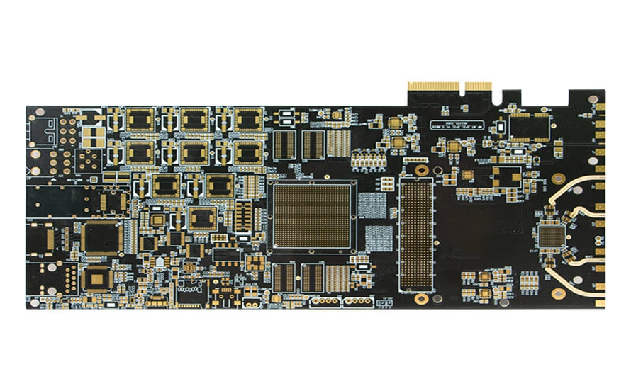
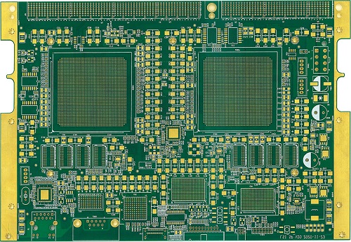
Technical Capability for China PCB Prototyping
For global innovators and engineers, China’s electronics manufacturing ecosystem offers unparalleled speed and value. However, navigating it to find a partner who delivers both superb quality and reliable small-batch production can be a challenge. EBest Circuit (Best Technology) stands apart by combining state-of-the-art facilities with deep engineering expertise, specifically tailored for prototyping and low-volume manufacturing.
1. The Foundation: Advanced FR4 & HDI Prototyping
This is the core of our rapid-turn prototyping services, where speed meets uncompromised quality.
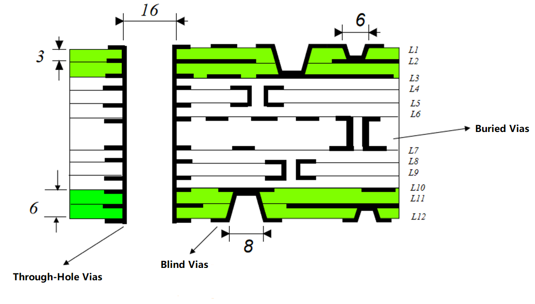
- Rapid Layer Stack-up: We expertly manufacture boards from 1 to 32 layers, with standard lead times. For designs requiring enhanced reliability (8 layers and above), we recommend and utilize high-Tg materials by default.
- Material Science: We offer a full spectrum of FR4 materials:
- Standard to High TG (130°C – 180°C): From KB 6160 to IT180 and S1170.
- Specialty Materials: Ready access to high-speed/low-loss (Rogers, Isola), high-CTI, and halogen-free materials to meet your specific electrical and environmental requirements.
- Pushing Density Limits (HDI): Our HDI capabilities are ideal for complex designs like processors, RF modules, and wearable devices.
- Laser Microvias: Down to 0.10mm diameter.
- Fine Line/Spacing: 3/3 mil (75µm) for dense circuit routing.
- Any-Layer Interconnect: Support for complex blind and buried via structures.
- Precision in Every Detail:
- Copper Weights: Inner layer (0.5 – 20 oz), Outer layer (0.5 – 28 oz).
- Drilling: Minimum mechanical drill size of 0.15mm with high aspect ratios up to 12:1.
- Tolerances: Tight registration control (±0.076mm) ensures perfect layer-to-layer alignment.
2. Flexibility for Innovative Designs: FPC & Rigid-Flex
When your product bends, folds, or fits into tight spaces, our flexible circuit solutions provide the answer.
- Unmatched Flexibility: We produce Flexible PCBs (FPC) up to 30 layers and large formats (e.g., 500mm x 2000mm for single-layer).
- Superior Fine-Line Technology: Consistent 2/2 mil (50µm) line/space capability.
- Rigid-Flex Integration: Combining rigid and flexible substrates into a single, reliable unit (2 to 50 layers), simplifying assembly and enhancing product durability.
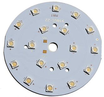
3. Power & Thermal Management: Heavy Copper & Metal-Core PCBs (MCPCB)
Prototype with confidence for high-power applications.
- Heavy Copper PCBs: Capable of 20 oz inner-layer copper for extreme current-carrying capacity and thermal endurance.
- Metal-Core PCBs (Aluminum, Copper): Ideal for LED lighting and power converters. We handle large panels up to 610mm x 1625mm with thermal conductivity up to 12 W/m.K.
4. Extreme Environment & High-Frequency Solutions: Ceramic Substrates
For applications where standard PCB materials fail, our ceramic substrate division delivers exceptional performance.
- DPC (Direct Plated Copper): The choice for ultra-fine features (50/50 µm line/space) and excellent thermal conductivity. Perfect for RF/Microwave and laser modules.
- DBC/AMB (Direct Bonded Copper/Active Metal Brazing): For the ultimate in thermal performance and power cycling reliability, with copper thicknesses from 100µm to 1200µm. Essential for power semiconductor packaging (e.g., IGBTs, SiC, GaN).
- LTCC/HTCC (Low/High-Temperature Cofired Ceramic): For creating miniature, highly integrated 3D interconnect structures capable of withstanding extreme temperatures and high frequencies.
5. Commitment to Quality & Precision Manufacturing
“Superb Quality” is embedded in every process.
- Comprehensive Surface Finishes: A full range of finishes including ENIG, ENEPIG, HASL, OSP, Immersion Silver/Tin, and selective/hard gold plating.
- Stringent Quality Control: Advanced testing capabilities including Impedance Control (±5%), Automated Optical Inspection (AOI), and Electrical Testing.
- Design for Manufacturability (DFM): Our engineering team provides proactive DFM feedback to ensure your prototype is not only manufacturable but optimized for performance and yield.
At EBest Circuit (Best Technology), we understand that a prototype is more than a board; it’s the first physical manifestation of your idea. Our comprehensive technical capabilities, focused on precision, quality, and fast turnaround, are designed to support you from initial concept through to pilot runs. We are the trusted partner for engineers worldwide who will not compromise on quality, especially in the critical prototyping phase.
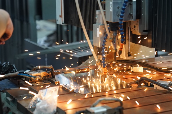
PCB Prototyping Machines
PCB prototyping machines form the backbone of modern electronics fabrication, transforming digital schematics into physical circuit boards within hours. These machines combine precision engineering with automated control to accelerate the PCB prototyping and prototype PCB manufacturing processes—where time, accuracy, and consistency are paramount.
Types of PCB Prototyping Machines
Laser Direct Imaging (LDI): This equipment uses high-resolution lasers to expose circuit patterns directly onto photoresist-coated copper laminates. LDI eliminates the need for film, ensuring ultra-fine trace accuracy—essential for HDI and microvia boards.
Automated Optical Inspection (AOI): After imaging and etching, AOI machines scan each layer using high-definition cameras to detect open circuits, shorts, and alignment errors. This automated check prevents downstream failures during prototype PCB assembly.
Drilling and Routing Machines: CNC-controlled drilling units create precise via holes, while routing machines cut the final panels into individual boards. High-speed spindles and laser alignment systems ensure every hole lands exactly where it should.
Electrical Testers: Flying-probe or bed-of-nails testers validate the continuity and isolation of every net. This verification step ensures that each prototyping PCB board performs as intended before soldering or component mounting.
Solder Mask and Silkscreen Printers: Advanced prototyping lines use automated printers to apply solder mask and component legends with perfect registration, improving readability and durability.
The Role of Automation in Rapid Development
What distinguishes today’s PCB prototyping machines from older systems is their integration and automation. From imaging to electrical testing, machines communicate through MES (Manufacturing Execution Systems) to track and control each stage. This connectivity reduces manual handling, shortens setup time, and enhances repeatability—key to delivering identical boards across multiple prototyping & small-batch PCB runs.
Automation also supports iterative development. Engineers can upload design revisions directly from CAD tools, initiate immediate production, and receive verified boards within a few days. This flexibility shortens design cycles and speeds product validation, giving companies a critical competitive edge in fast-paced markets.
Why Machine Investment Defines Quality
In prototype PCB manufacturing, machine capability directly determines precision, turnaround time, and overall quality. Factories equipped with advanced LDI, AOI, and automated routing systems can achieve finer traces, cleaner vias, and better impedance control—essential for high-speed or RF designs.
At EBest Circuit (Best Technology), continual investment in modern PCB prototyping machines enables consistent accuracy and shorter delivery cycles. This ensures that every prototype board aligns with final production standards, enabling a seamless transition from testing to market.”
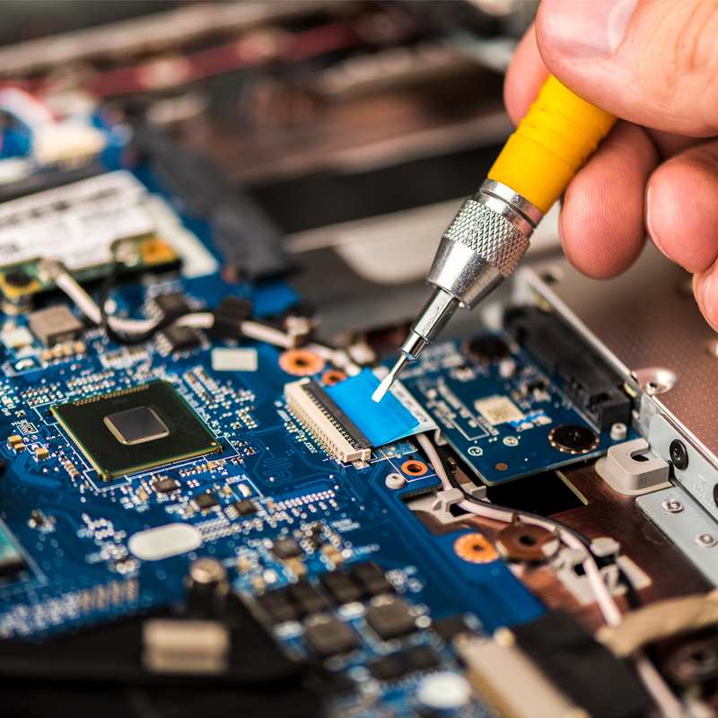
PCB Prototype Board How to Use?
Understanding the workflow after you receive your PCB prototype board is key to effective testing.
- Inspection: First, visually inspect the board against your design files. Check for obvious defects in soldermask, silkscreen, and pad alignment.
- Assembly: Carefully solder all your components (ICs, resistors, connectors) onto the board. For complex boards, a stencil and reflow oven are recommended for best results.
- Power-Up and Testing: Before applying full power, check for short circuits. Then, power up the board and use multimeters and oscilloscopes to test voltages, signals, and functionality against your design expectations.
This hands-on phase is where the theoretical design meets reality, and any issues found will inform the next iteration of your prototyping pcb cycle.
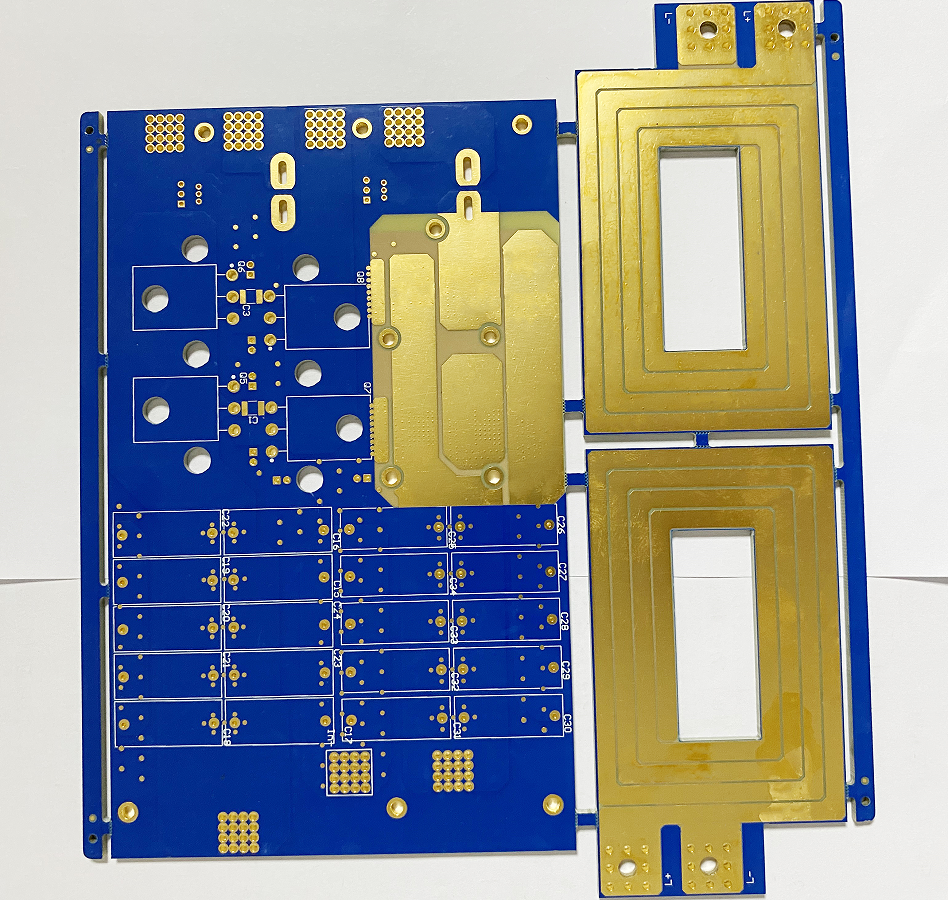
Case of Prototyping PCB Board at EBest Circuit (Best Technology)
At EBest Circuit (Best Technology), we specialize in transforming complex design specifications into high-quality, reliable prototype PCBs. This case study details the manufacturing process and technical considerations for a specific 4-layer FR4 board, showcasing our capability to meet stringent industry standards and deliver for mission-critical applications.
Project Overview & Customer Requirements
A customer approached us with a requirement for a high-reliability 4-layer prototype PCB. The board was designed for an aerospace application, necessitating strict adherence to quality controls and comprehensive documentation. The key requirements were:
- High-Reliability Standard: Production must comply with IPC-6012 and IPC-A-600 Class 3 specifications.
- Full Traceability: A First Article Inspection Report (FAIR) and Certificate of Conformance (COC) with batch/serial numbers were required, following AS9100 process controls.
- Design for Automated Assembly: The board included breakaway tab rails and fiducial marks to ensure compatibility with high-precision SMT assembly lines.
EBest Circuit (Best Technology)’s Manufacturing Strategy & Execution
To meet these requirements, our engineering and production teams executed a precise manufacturing strategy:
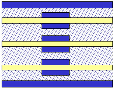
- Material Selection and Layer Stack-up:
- We selected FR4 material with a Tg of 150°C to ensure thermal stability and mechanical strength suitable for the operating environment.
- A balanced 4-layer stack-up was implemented, with a 1.6mm finished thickness, to provide dedicated power and ground planes for optimal signal integrity and power distribution.
- Precision Imaging and Lamination:
- Inner layer cores with 0.5 oz copper were processed using our high-precision laser direct imaging (LDI) systems to achieve the required circuit patterns.
- The layers were laminated under controlled temperature and pressure to prevent delamination and ensure perfect registration, a critical factor for Class 3 reliability.
- Controlled Drilling and Plating:
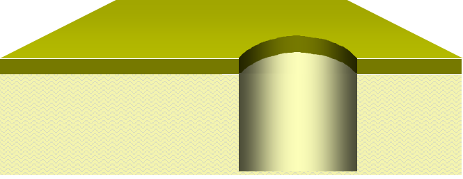
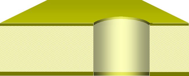
- Mechanical drilling was performed to create the vias. As per the specification, all vias were tented with solder mask in the subsequent process to protect them from contamination and potential solder shorts.
- Surface Finish Application:
- We applied Immersion Silver (ImAg) as the final surface finish. This choice provided excellent flatness for fine-pitch component soldering and reliable performance for the intended application.
- Solder Mask and Silkscreen:
- Green LPI solder mask was applied to both sides, with precise openings for the fiducial marks and components.
- White silkscreen was used for component designators and logos, ensuring clear legibility.
- Panelization and Fiducial Creation:
- The individual boards were panelized with 10mm breakaway tab rails on all four sides to facilitate secure handling during assembly.
- Global fiducial marks (2mm copper pads with 3mm solder mask openings) were added to the top and bottom layers, positioned 5mm from the board edge and 15mm from each corner, as specified.
- Quality Assurance and Documentation:
- Throughout the process, in-line inspections and electrical testing were conducted.
- Upon completion, a comprehensive FAIR was generated, verifying that every parameter met the IPC Class 3 requirements.
- A COC including the unique production batch and serial number was issued, fulfilling the AS9100 traceability requirement.
PCB Specification Summary
- Layer Count: 4 Layers
- Base Material: FR4, Tg 150°C
- Finished Board Thickness: 1.6mm ±10%
- Copper Weights: Outer Layers: 1 oz; Inner Layers: 0.5 oz
- Solder Mask: Green, LPI
- Silkscreen: White
- Surface Finish: Immersion Silver (ImAg)
- Via Treatment: All vias tented with solder mask
- Board Edges: 10mm breakaway tab rails on all four sides
- Fiducial Marks: Two global fiducials per side (top and bottom). Shape: 2mm diameter copper pad with 3mm diameter solder mask opening. Location: 5mm from board edge, 15mm from each corner.
- Quality Standard: Manufactured in strict compliance with IPC-A-600 and IPC-6012 Class 3 requirements.
- Documentation: FAIR (First Article Inspection Report) and COC (Certificate of Conformance) with production batch/serial number, following AS9100 requirements.
In summary, this project exemplifies EBest Circuit (Best Technology)’s commitment to producing prototype PCBs that are not just functional but are built to the highest standards of quality and reliability. By combining advanced manufacturing capabilities with rigorous quality control and comprehensive documentation, we provide our customers with the confidence that their prototypes will perform as expected, even in the most demanding applications. We are the trusted partner for turning sophisticated designs into reality.
Why Choose EBest Circuit (Best Technology) for Prototyping & Small-Batch PCBs?
Why choose EBest Circuit (Best Technology) for prototyping & small-batch PCBs? The answer lies in our unwavering commitment to being a true partner in your success. We combine the cost and technical advantages of a leading Chinese manufacturer with the service quality and reliability you deserve.
- Superior Quality and Consistency: Our rigorous quality management system ensures every board, from a single prototype to a small-batch order, meets the highest standards.
- Expert Technical Support: Our engineering team provides proactive support, offering DFM suggestions and helping you navigate complex design challenges for both standard and advanced prototype PCB assembly.
- Transparent Pricing and Fast Turnarounds: We offer transparent pricing without compromising on speed, ensuring you get the best value and your project stays on track.
- Advanced Manufacturing Capabilities: From simple double-layer boards to complex HDI and ceramic substrates, our technical capability for China PCB prototyping is first-class.
- Seamless Customer Experience: We make the process of ordering PCB prototype online simple and transparent, with clear communication at every step.
Prototyping & small-batch PCBs form the critical bridge between a conceptual design and a successful electronic product, enabling thorough testing and iterative improvement. This guide has outlined the key considerations, from definitions and global comparisons to the practicalities of machinery and board testing. For engineers and innovators seeking a partner that delivers on quality, reliability, and advanced prototype PCB manufacturing capabilities, BEST Technology stands ready to support your journey from idea to reality. Reach out to our team at sales@bestpcbs.com to get a quote for your next project.