pcb
Home > Blog

Posts Tagged ‘PCBA’

What is pcb board assembly? PCB assembly manufacturer
星期四, 2 1 月, 2025

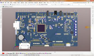
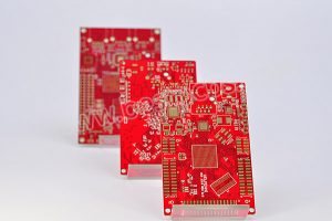
What is pcb board assembly? PCB board assembly is the process of installing various electronic components (such as resistors, capacitors, chips, etc.) on the PCB and achieving electrical connections through welding and other methods to build a circuit board that can achieve specific electronic functions. This process includes component preparation, PCB board pretreatment, welding and post-assembly inspection.

What is the assembly of a PCB?

What is pcb board assembly? PCB assembly manufacturer

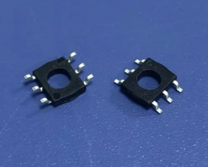
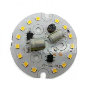
PCB assembly is the process of installing and electrically connecting various electronic components to a printed circuit board according to design requirements. It includes component preparation (purchase inspection, classified storage), PCB preparation (inspection, cleaning), welding (plug-in welding and patch welding) and post-assembly inspection (appearance and electrical performance inspection). Its quality is crucial to the performance and reliability of electronic products and is widely used in consumer electronics, industrial control, communications, automotive electronics and other fields.

How do you assemble a PCB board?

  • Component preparation: Purchase electronic components according to design documents and check whether the component specifications, models and appearance are qualified. After that, the qualified components are classified and stored by type, packaging form, etc.
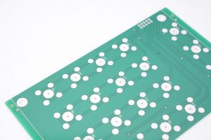
  • PCB preparation: Check the appearance of the PCB board for scratches, short circuits and other defects, and wipe it with a special cleaner or alcohol to ensure that the surface is free of oil and dust, and that the pads are flat and free of oxidation.
  • Soldering process: Insert the component pins into the corresponding holes of the PCB, use an electric soldering iron to melt the solder to fill the pins and pads to form solder joints, and pay attention to controlling the temperature and time.
  • SMT soldering: Print solder paste on the PCB pads, place the components with a SMT machine, and then heat them according to the temperature curve through a reflow oven to melt the solder paste to form solder joints.
  • Post-assembly inspection: Perform an appearance inspection to check the solder joints and component installation. Then perform an electrical performance test, use professional equipment to check whether the function is normal, and troubleshoot and repair the faults.

What is the function of PCB assembly?

The main functions of PCB assembly include the following aspects:

  • Electrical connection: The copper wire tracks on the PCB board can connect various electronic components (such as resistors, capacitors, and integrated circuits) to form a complete circuit system. This efficient connection method simplifies circuit design and improves circuit reliability.
  • Component support: PCB provides stable support for components. Through welding and other methods, components can be firmly mounted on PCB, which improves the structural integrity and portability of the equipment.
What is pcb board assembly? PCB assembly manufacturer
  • Circuit protection: The insulating material of PCB can effectively isolate electromagnetic interference and protect the circuit from the external environment (such as moisture, dust, etc.), thereby extending the service life of electronic equipment, especially in harsh industrial environments.
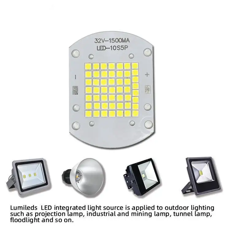
  • Heat dissipation function: In high-performance, high-power electronic equipment, the metal layer (such as copper foil) on the PCB can quickly absorb and disperse the heat generated when the circuit is working, preventing components from being damaged by overheating. By optimizing the design, such as increasing the thickness and layout of the copper foil, the heat dissipation efficiency can be further improved.
  • Space optimization and compact structure: The design of the PCB is not only related to the functional realization of the circuit, but also affects the production cost, production efficiency and subsequent maintenance and replacement. Optimizing the use of space makes the internal structure of electronic equipment more compact and beautiful.

What is the standard for PCB assembly?

The standardization of PCB assembly is one of the important measures to ensure product quality and reliability. The following are the main standards for PCB assembly:

  • PCB board size and positioning: The size and positioning of the PCB board should meet the design requirements to ensure accurate alignment and fixation during the assembly process.
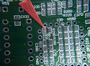
  • Component welding quality: The quality of the welding point is the key. The welding point should be smooth, firm, and burr-free to avoid poor welding, cold welding and other undesirable phenomena.
  • Component arrangement and layout: The arrangement and layout of the components should meet the design requirements to ensure the correct spacing and position between the components to avoid mutual interference.
  • Solder point quality: The solder joint should be firm, smooth, and burr-free to ensure the normal operation of the circuit.
  • Appearance quality: The surface of the PCB board should be clean, flat, and scratch-free, and the components should be arranged neatly and beautifully.
  • Electrical performance: Ensure that the electrical performance of the PCB after assembly meets the design requirements.
  • Weather resistance: PCB assembly should have good weather resistance and be able to work stably under different environmental conditions.
  • Reliability: The durability and reliability of the components should be considered during the assembly process to ensure stability in long-term use.

In addition, the specific assembly standards may vary depending on different application scenarios and product types. During the assembly process, relevant standards and requirements should be followed to ensure the quality and stability of the assembly.

What files are needed for PCB assembly?

The following main files are needed in the PCB assembly process:

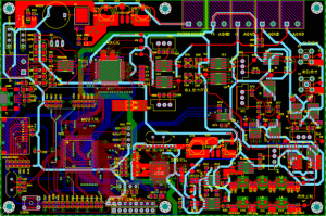
  • Gerber file: This is the most critical file in PCB production, which contains the geometric information of each layer of the circuit board, such as copper lines, pads, solder mask and silk screen layers. Gerber files are usually generated by CAD software and saved in a standard format.
  • Drill file (.drl or .xin): This file provides the location and size information of all the drill holes on the circuit board, ensuring that the drill holes are accurately aligned with the circuit pattern.
  • Bill of Materials (BOM): The BOM lists all the materials and components that make up the circuit board, including their quantity, specifications and supplier information.
  • Coordinate files: These files provide the coordinate and orientation information of each component on the circuit board, which is essential for the automated assembly process.
  • Assembly drawings: If the PCB needs to be assembled with other electronic components, it is necessary to provide assembly drawings or assembly instructions, which detail how the components are installed on the circuit board.
  • Test requirements: If the manufacturer is required to perform specific tests, such as functional tests or electrical performance tests, it is necessary to provide test requirements or test instructions files.
  • Design Rule Check File (DRC): Used to verify whether the PCB design meets the manufacturing requirements and standards, helping to find and correct potential problems during the design stage.
  • 3D Model (STEP File): Used to generate a 3D model of the circuit board to help simulate and verify during the production process.
  • Structure Drawing (DXF format): Used to make a CAD structure drawing of the circuit board to ensure accuracy during the manufacturing process.

When providing these files, make sure they are up-to-date, accurate, and match the production requirements. It is also very important to maintain communication with the manufacturer to ensure that they have a clear understanding of the design requirements and can produce as expected.

What are the materials used in PCB assembly?

PCB assembly mainly uses the following materials:

1. Electronic components

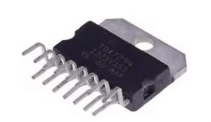
  • Passive components: including resistors (used to control current and voltage, with a variety of resistance values, powers and packaging forms), capacitors (used to store charge and filter, there are ceramic, electrolytic, tantalum capacitors and other types, with different capacities and withstand voltage values), inductors (used to store magnetic field energy, with winding and stacked inductors, and the unit of inductance is Henry).
What is pcb board assembly? PCB assembly manufacturer
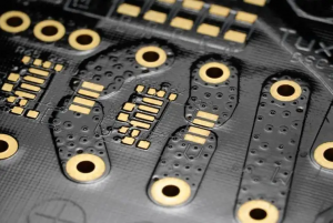
  • Active components: such as integrated circuits (including various functional circuits, with DIP, SOP, BGA and other packaging forms), transistors (used for amplification and switching functions, with BJT and FET and other types, with different parameters).

2. Welding materials

  • Solder wire: The main component is tin-lead or lead-free alloy, with different diameters, lead-containing solder wire has a lower melting point, lead-free solder wire has a higher melting point, and often contains flux inside.
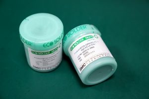
  • Solder paste: used for SMT welding, it is a mixture of solder powder and flux, and its viscosity and metal content affect the quality of printing and welding.
  • Flux: used to remove metal surface oxides and reduce solder surface tension, available in liquid, paste and other forms, and ingredients include organic acids, rosin, etc.

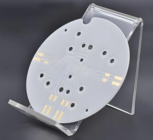
3. PCB substrate materials

  • FR-4: Commonly used epoxy glass fiber cloth laminate, with good insulation, mechanical strength and thermal stability, and different thicknesses.
  • Ceramic substrate: excellent thermal conductivity and high-frequency performance, such as aluminum nitride and alumina ceramic substrates, suitable for high-power and high-frequency devices.
  • Flexible PCB substrate: used for bendable or foldable devices, the material is soft, and polyimide is often used as an insulating layer.

4. Other auxiliary materials

  • Cleaning agent: used to clean impurities on PCB boards, including alcohol and special electronic cleaning agents.
  • Thermal conductive materials: such as thermal grease and thermal conductive tape, used for heat dissipation of high-power components.

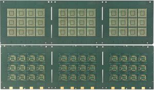
How is a PCB board structured?

The basic structure of a PCB board includes multiple layers, each of which has its specific functions and effects.

PCB boards are mainly composed of the following layers:

  • Top Layer: This is the top layer of the PCB board, which is usually filled with electronic components such as resistors, capacitors, and chips. The top layer not only carries these components, but also is responsible for their connection and wiring to ensure that current and signals can be accurately transmitted.
  • Bottom Layer: Located at the bottom of the PCB board, it is mainly responsible for the laying of ground wires and the connection of auxiliary signal lines. The bottom layer provides a solid support for the circuit board to ensure the stability and safety of the circuit.
  • Inner Layer: Located between the top layer and the bottom layer, it is composed of multiple layers of copper foil stacked to form a complex circuit network. The inner layer is used to conduct signals and power supply, reduce signal interference, and ensure the clarity and accuracy of the signal.
  • Solder Mask Layer: This is a special layer, the main function of which is to protect the pads on the circuit board, prevent the solder from splashing into other areas during the soldering process, and ensure the soldering quality and stability of the circuit.

What is the difference between PCB and PCB assembly?

The main difference between PCB and PCBA lies in their status and function.

1. Definition and function

  • PCB: PCB is the cornerstone of electronic devices, providing physical support and electrical connection for electronic components. It consists of a conductive copper layer and an insulating layer, and is usually manufactured by methods such as chemical etching. The PCB itself does not contain any electronic components, but is just an empty circuit board.
What is pcb board assembly? PCB assembly manufacturer
  • PCBA: Printed circuit board assembly refers to the installation of electronic components on the PCB to form a complete circuit. PCBA is functional and can be directly installed in the final product for use.

2. Cost and complexity

  • PCB: Since there are no electronic components, the manufacturing process is relatively simple and the cost is low.
  • PCBA: Due to the need to install and test electronic components, the manufacturing process is more complicated and the cost is higher. PCBA is more complex and more expensive than PCB.

3. Application

  • PCB: Mainly used to manufacture PCBA, as a support and connection frame for electronic components.
  • PCBA: After assembly, PCBA is used in various electronic devices such as computers, smartphones, home appliances, etc.

In summary, PCB board assembly is an interlocking, delicate and complex process. From the careful selection of component preparation, to the pretreatment of PCB boards, and the final strict control, each step should not be underestimated. It organically integrates various electronic components with PCB boards to become PCBA.

You may also like

Why Ceramic Substrate PCB Is Gaining Popularity?
星期一, 30 12 月, 2024

Ceramic substrate PCB is a crucial component in modern electronics, offering significant advantages in applications requiring high thermal conductivity, electrical insulation, and mechanical strength. In this blog, we will delve into the various aspects of ceramic substrate PCB, explaining its materials, benefits, and applications, and explore how it compare to traditional FR4-based PCB. Whether you are new to PCB design or an experienced engineer, this guide will help you understand why ceramic substrate PCB is gaining popularity.

What is Ceramic Substrate PCB?

Ceramic substrate PCB or ceramic PCB is a type of printed circuit board that uses ceramic materials as the base substrate. Unlike traditional PCBs, which are usually made of fiberglass (FR4), ceramic substrate PCB is designed to handle high thermal stresses and provide better electrical insulation properties. This PCB is commonly used in industries like telecommunications, automotive, medical devices, and power electronics due to their exceptional thermal management capabilities and durability.

The main advantage of ceramic substrate PCBs is their ability to dissipate heat efficiently, which is vital in applications where heat management is a critical factor. Ceramic materials, such as alumina (Al₂O₃), aluminum nitride (AlN), and beryllium oxide (BeO), are known for their excellent heat conductivity, making them ideal for high-power electronics.

What is the Best Substrate for PCB?

The best substrate for a PCB depends on the specific application and the requirements of the circuit. For general-purpose electronics, FR4 is the most commonly used substrate due to its balance of cost and performance. However, for applications that demand superior thermal conductivity, high-frequency performance, or electrical insulation, ceramic substrates are often the preferred choice.

Ceramic substrates are especially suitable for high-power, high-frequency, and high-temperature environments. These materials offer lower thermal expansion rates, higher thermal conductivity, and better resistance to extreme conditions than traditional PCB materials. Therefore, in scenarios where heat management is paramount, such as power amplifiers or LED lighting, ceramic PCBs are the best option.

What Material is Commonly Used for PCBs?

The material commonly used for PCBs can vary depending on the application. The most popular materials include:

FR4 (Fiberglass Reinforced Epoxy): This is the most common PCB material, primarily used for general electronic applications. It is affordable and offers decent mechanical and electrical properties.
Ceramic: As discussed, ceramic materials such as alumina, aluminum nitride, and beryllium oxide are used in high-performance PCBs. They are particularly suited for thermal management and high-frequency applications.
Polyimide: Used for flexible PCBs, polyimide provides excellent resistance to heat and harsh chemicals.
Teflon: Ideal for high-frequency circuits, Teflon offers low signal loss and excellent electrical insulation.

While FR4 is suitable for most basic applications, ceramic substrates stand out when specific performance characteristics like high thermal conductivity or resistance to high temperatures are needed.

Which PCB Substrate Has High Thermal Conductivity?

Ceramic PCBs are known for their superior thermal conductivity compared to other PCB materials. Materials like aluminum nitride (AlN) and boron nitride (BN) have the highest thermal conductivity, making them ideal for high-power applications where heat dissipation is crucial.

Aluminum nitride, for instance, offers thermal conductivity values between 170-200 W/mK, which is significantly higher than that of FR4, which typically ranges around 0.3 W/mK. This makes ceramic substrates the go-to choice for applications such as power electronics, LED lights, and other high-heat applications where heat needs to be efficiently transferred away from the components.

What is the Thermal Conductivity of Ceramic PCB?

The thermal conductivity of ceramic PCBs can vary depending on the material used. The most common ceramic materials include:

Alumina (Al₂O₃): This is one of the most frequently used materials in ceramic PCBs. Alumina has a thermal conductivity ranging from 20 to 30 W/mK, making it suitable for medium-to-high-power applications.
Aluminum Nitride (AlN): Aluminum nitride has a much higher thermal conductivity, typically around 170-200 W/mK. This makes it ideal for high-power applications, especially in areas where rapid heat dissipation is needed.
Beryllium Oxide (BeO): While less commonly used due to safety concerns (due to the toxic nature of beryllium), Beryllium oxide offers very high thermal conductivity, around 250-300 W/mK.

When compared to other PCB materials, ceramic substrates offer a distinct advantage in terms of their heat management capabilities. They ensure that sensitive components remain within their operating temperature range, extending their lifespan and improving performance.

How Thick is Ceramic PCB?

The thickness of a ceramic PCB can vary depending on the design requirements and the specific material used. Typically, ceramic PCBs can range from 0.2 mm to 2 mm in thickness, but in some cases, they can be made thicker or thinner to suit specific needs.

The thickness of the PCB plays a role in both its mechanical strength and thermal properties. Thicker ceramics tend to offer better heat dissipation, but they may be more rigid and difficult to process. On the other hand, thinner ceramics are more flexible but may not handle as much thermal stress. The optimal thickness depends on the application and the required performance characteristics of the circuit.

What is the Difference Between Ceramic Substrate and FR4?

The primary difference between ceramic substrates and FR4 PCBs lies in their material properties and performance characteristics.

Thermal Management: Ceramic substrates excel in heat dissipation, with materials like aluminum nitride offering significantly higher thermal conductivity than FR4. This makes ceramics the better choice for high-power applications.
Electrical Insulation: Ceramic substrates provide superior electrical insulation compared to FR4, making them ideal for applications requiring high voltage isolation.
Mechanical Properties: Ceramic PCBs are often more rigid and can withstand higher temperatures than FR4-based boards, making them suitable for demanding environments.
Cost: FR4 is much cheaper to produce than ceramic substrates, making it the go-to material for mass-produced electronics. However, when performance is the priority, ceramic PCBs provide a much better solution, despite their higher cost.

Overall, the choice between ceramic and FR4 substrates depends on the specific needs of the project. If thermal management, high-frequency performance, or electrical insulation is critical, ceramic substrates are often the better option.

What is Ceramic Board Used For?

Ceramic boards, or ceramic PCBs, are widely used in applications where thermal conductivity, electrical insulation, and mechanical strength are critical. Some of the most common applications of ceramic PCBs include:

Power Electronics: Ceramic PCBs are used in power supplies, inverters, and other high-power circuits, where heat dissipation is crucial for reliable operation.
LED Lighting: Ceramic substrates are used in LED modules, where efficient heat management is essential for preventing thermal damage to the LEDs and improving their lifespan.
Telecommunications: In high-frequency communication equipment, ceramic PCBs help ensure signal integrity and manage heat effectively.
Automotive: Ceramic PCBs are used in automotive electronics, including control systems, power modules, and sensors, which require high thermal conductivity and reliability in harsh environments.
Medical Devices: Ceramic PCBs are used in medical devices such as MRI machines and pacemakers, where high precision and reliability are essential.

The versatility of ceramic PCBs makes them an excellent choice for any application where performance, thermal management, and durability are essential.

Ceramic substrate PCBs play a vital role in modern electronics, offering superior thermal conductivity, electrical insulation, and mechanical strength compared to traditional FR4-based boards. They are essential in high-power, high-frequency, and high-temperature applications, ensuring that sensitive components operate within their optimal temperature range. While ceramic PCBs tend to be more expensive than FR4, their performance benefits make them the go-to solution for industries where reliability and performance are paramount.

Choosing ceramic PCBs can elevate your designs, particularly when heat management and durability are top priorities. If your application demands top-tier performance, ceramic substrates are a smart investment that ensures long-lasting and efficient operation.

As a ceramic PCB manufacturer, Best Technology specialize in providing high-quality ceramic PCBs tailored to your specific needs. With our advanced manufacturing processes and expert team, we ensure that every PCB we produce meets the highest standards of performance and reliability. If you are looking for dependable ceramic substrate manufacturers, contact us today at sales@bestpcbs.com to learn more about how we can help with your next project.

You may also like

Let you know about refrigerator pcb
星期一, 23 12 月, 2024

What is a refrigerator pcb? Refrigerator PCB is usually composed of insulating substrate, copper foil circuit and various electronic components. Insulating substrate provides support for circuits and components. Common materials include epoxy glass fiber board, which has good insulation performance, mechanical strength and stability, and can adapt to the complex environment inside the refrigerator.

Do refrigerators have PCBs?

There are PCBs inside refrigerators. The PCB of a refrigerator is one of the core control components of the refrigerator, usually called the computer version or control board of the refrigerator. It is responsible for controlling various functions of the refrigerator, such as refrigeration, preservation, energy saving, etc. It monitors and adjusts the operating status of the refrigerator in real time through sensors and control systems to ensure that the refrigerator can work efficiently and stably.

Let you know about refrigerator pcb

What is a PCB in a fridge?

The PCB in a refrigerator is an important part of the refrigerator control system. The role of PCB in a refrigerator mainly includes the following aspects:

  • Connection and control: As the core of the refrigerator control system, PCB controls the switch and operation of the refrigerator by connecting various sensors and other electrical components. It integrates various sensors, such as temperature sensors and humidity sensors, to provide real-time feedback on the temperature and humidity conditions in the refrigerator, thereby achieving automatic control.
  • Interactive function: PCB can interact with users through alarm lights, buzzers and displays to control various functions of the refrigerator, such as constant temperature, refrigeration and thawing.
  • Intelligent function: For high-end refrigerators, PCB can also achieve more functions and information feedback by connecting to the Internet. For example, users can remotely control the refrigerator through mobile phone APP, set the laundry program in advance or let the sweeping robot start working, etc.
  • Maintenance: In order to ensure the normal operation of PCB, it is necessary to clean and inspect it regularly, and ensure that its installation location is dry and ventilated to avoid moisture. In addition, avoid changing the temperature and appliance settings at will to avoid affecting automatic control.

What role do PCBs play in refrigerators?

The role of PCB in refrigerators mainly includes controlling various functions of refrigerators, processing sensor signals, realizing the interconnection of home appliances and improving the intelligence level of refrigerators.

1. Control various functions of refrigerators

PCB is one of the core control components of refrigerators, responsible for controlling various functions of refrigerators, such as refrigeration, preservation, energy saving, etc. Through sensors and control systems, PCB can monitor and adjust the operating status of refrigerators in real time to ensure that refrigerators can work efficiently and stably.

Let you know about refrigerator pcb

2. Processing sensor signals

PCB smart home appliance board is responsible for processing signals from various sensors, such as temperature sensors and humidity sensors in refrigerators. Through accurate analysis and processing of these signals, smart home appliance board can automatically adjust the operating status of home appliances according to preset programs.

3. Realize the interconnection of home appliances

PCB smart home appliance board also realizes the interconnection of home appliances. With the help of network module, smart home appliances can be connected to the home wireless network, and users can remotely control home appliances through mobile phone APP.

Can refrigerator PCB be repaired?

Refrigerator PCB (Printed Circuit Board) can be repaired. If the PCB of the refrigerator fails, you can take the following steps to repair it:

  • Check the warranty period: First check whether the refrigerator is within the warranty period. If it is within the warranty period, you can contact after-sales for free repair or replacement.
  • Self-inspection and simple repair: For some simple problems, you can check and repair them yourself. If the refrigerator does not run after power on, you can check whether the fuse, plug, temperature controller contacts, etc. are normal.
  • Replace PCB: If the PCB is severely damaged, you may need to replace the entire PCB. You can buy an identical PCB to replace it yourself, but you need to be careful when disassembling it, especially not to damage other components.

What is the common damage of a refrigerator?

Common causes of refrigerator PCB damage mainly include the following:

  • Overvoltage: The working voltage of the refrigerator circuit board is 220V. If the voltage is too high, the circuit board will be overloaded and damaged. It is recommended to use a socket with stable voltage or a voltage stabilizer to protect the circuit board.
  • Overload: Hanging items on the refrigerator or placing heavy objects on its door will cause the door to be poorly sealed, air circulation to be blocked, and the refrigerator to work abnormally, which will lead to circuit board overload.
Let you know about refrigerator pcb
  • Sudden power outage: Sudden power outage or lightning may cause damage to the refrigerator circuit board. In case of power outage or bad weather, it is recommended to disconnect the power supply or use a protective device.
  • Poor heat dissipation: The temperature of the refrigerator compressor continues to rise, and it cannot dissipate heat in time, which will burn out the fuse and other components, causing damage to the refrigerator circuit board.
  • Unstable voltage: Unstable voltage cannot meet the power used by the refrigerator, which will cause damage to the refrigerator circuit board. It is recommended to install a voltage stabilizer to protect the circuit board.

How much does it cost to replace a circuit board in a refrigerator?

The cost of replacing a circuit board in a refrigerator is affected by many factors:

  • Refrigerator brand and model: The design, function and complexity of the circuit board of refrigerators of different brands and models vary greatly, and the price will also vary greatly. The circuit boards of high-end brands or refrigerators with complex functions are usually more advanced, more sophisticated and more expensive.
  • Fault severity: If only individual components on the circuit board are damaged, the problem can be solved by repairing and replacing the components, and the cost is relatively low; but if the circuit board has serious problems such as short circuits and burns, the entire circuit board needs to be replaced, and the cost will increase significantly.

How much does it cost to repair a PCB?

The cost of repairing a PCB is affected by many factors, as follows:

1. Fault type

  • Component damage: If only individual ordinary components are damaged, such as capacitors and resistors, the repair is relatively simple and the cost is low; if key components such as chips are damaged, the repair is difficult and the cost will increase significantly.
  • Circuit problem: The difficulty of repairing a circuit break or short circuit varies depending on the complexity of the circuit. The cost of repairing a simple circuit is low, and the cost of repairing a circuit problem on a multi-layer board or high-density circuit board is high.
  • Solder joint problem: It is relatively easy to repair the cold soldering and desoldering of a small number of solder joints, and the cost is not high; but if a large number of solder joints have problems or the solder joints are located in important parts such as chips, the repair cost will increase.
  • Software failure: For the PCB boards of some smart devices, if there are software failures, professional software engineers are required to debug and repair them, which may increase the repair cost.

2. Circuit board type

  • Computer motherboard: The repair of ordinary desktop computer motherboards is relatively common and easy, and the cost is average; while the notebook motherboard has high integration and complex structure, which is difficult to repair and the cost is usually high.
  • Mobile phone motherboard: Mobile phone motherboards are small in size and highly integrated. Repair requires high-precision equipment and technology, and mobile phones are updated quickly. The repair costs of motherboards of different models vary greatly.
  • Home appliance circuit boards: The circuit boards of common home appliances such as TVs, refrigerators, washing machines, etc. have relatively simple functions, and the repair costs are generally stable, but if they are circuit boards of high-end smart home appliances, the repair costs may be higher.
  • Industrial control circuit boards: Industrial control circuit boards have extremely high requirements for stability and reliability, and usually use high-quality components and complex designs. They are difficult to repair and costly.

How to customize refrigerator PCB?

Customizing refrigerator PCB requires the following steps:

  • Clear requirements: determine the functional requirements of the refrigerator, consider the use environment of the refrigerator, determine the PCB’s operating temperature range, humidity requirements, electromagnetic compatibility and other performance indicators.
  • Design circuit: According to the requirements, use professional design software to draw circuit diagrams, layout and wiring; plan the board layers reasonably. For refrigerator PCBs with complex functions, multi-layer board design can be used; consider the heat dissipation problem. For heating components, they should be laid out as close to the edge as possible, and heat sinks or heat dissipation holes can be added to ensure the temperature stability of the PCB during operation.
  • Select materials: According to the use environment and performance requirements of the refrigerator, select the appropriate substrate and the appropriate copper foil thickness to meet different current carrying capacity and signal transmission requirements. According to the electrical performance and environmental adaptability requirements, select the surface treatment process, etc.
Let you know about refrigerator pcb
  • Manufacturing and testing: During the manufacturing process, drilling holes needs to be accurately drilled, electroplating ensures the formation of a good conductive layer, etching removes excess copper foil, silk-screens clear and accurate symbols and component identification, and uses automated optical inspection equipment to quickly and accurately inspect the PCB. Electrical and functional tests are also performed to ensure that the PCB meets the design requirements and performance standards.
  • Assembly and debugging: Assemble electronic components onto the PCB through surface mount technology or through-hole technology, pay attention to welding quality, perform system debugging on the assembled PCB, check whether the various functions of the refrigerator are normally implemented, such as temperature control accuracy, start and stop and operation status of the refrigeration system, intelligent interconnection function, etc., and make timely adjustments and optimizations to any problems that arise.

As a key component of the refrigerator, the refrigerator PCB should be designed to take into account the special environment of the refrigerator, and be resistant to low temperature, humidity, and electromagnetic interference. BEST Technology will start from the design of the refrigerator PCB and customize the best solution based on the characteristics and needs of different refrigerators. In the production process, various process standards are strictly followed, and then the finished product is strictly tested to ensure the high quality of the PCB layer by layer.

You may also like

How are the circuit boards connected?
星期二, 17 12 月, 2024

How are the circuit boards connected? Soldering is the most common and long-standing way to connect circuit boards. For traditional circuit boards, we usually use electric soldering irons to perform soldering operations. First, the metal part of the electronic component pins or wires to be connected is tightly fitted with the corresponding pads on the circuit board. Then, the pads and pins are heated with an electric soldering iron, and the solder wire is brought close together to melt the solder and evenly wrap the connection parts to form a stable metal connection.

How are the circuit boards connected?

A circuit board 6 connections typically refers to a design that incorporates six distinct points or pads for electrical connections, which could be input/output ports, signal pathways, or power connections. These boards are often used in simple applications where a limited number of connections are needed to interface with other components or systems.

What are the connections between circuit boards?

The main ways to connect circuit boards include the following:

  • Welding connection: This is one of the most commonly used connection methods, which connects components on the circuit board together by welding. The advantages of welding connection are stable and reliable connection, low cost, and suitable for circuit boards that do not require regular changes.
  • Plug-in connection: Plug-in connection can achieve fast plug-in and pull-out, easy replacement and maintenance, but requires high precision of plug-ins and sockets, and occupies a large space, which is not suitable for circuit boards with limited space.
  • Connector connection: This is a widely used circuit board connection method that can connect circuit boards of different forms and sizes. The advantages of connectors are convenient and fast connection, high reliability, and a large number of plug-in and unplug times, which are suitable for various circuit board application scenarios.
  • Plug-in connection: widely used in complex instruments and equipment, and connected through standard pins or sockets. This method is easy to replace and repair, ensuring the reliability and production efficiency of the connection.
  • Special connection methods: including V-cut and copper foil bridge connection, spring connection and spring connection, panel connection, etc. These methods are suitable for specific scenarios and needs, such as V-cut for the separation stage of PCB boards, spring connection and spring connection for the connection of flexible circuit boards, and panel connection for multiple PCB designs placed on a large substrate.

How to connect components on PCB?

There are usually the following ways to connect components on PCB:

  • Soldering: This is the most common connection method. By connecting the pins of the components to the pads on the PCB with solder, you can use a soldering iron or SMT equipment for soldering.
  • Spring contact: For some components that need to be replaced frequently, such as batteries, you can use spring contact to make the components easy to disassemble.
How are the circuit boards connected?
  • Screw fixing: For components that need to withstand large forces, such as heat sinks, motors, etc., screw fixing can be used. Pay attention to choosing the right screws and tightening strength.
  • Clamping with pliers: For some components that need to be fine-tuned, such as rheostats, potentiometers, etc., pliers can be used to clamp.
  • Plastic bayonet: For some components that need to be frequently plugged and unplugged, such as wire connectors, plastic bayonet can be used for connection.

How to connect PCB boards together?

To connect PCB boards together, you can consider the following common methods:

Welding:

  • PCB wire welding: This is a simple and commonly used method to achieve connection by directly welding the wire to the pad of the PCB board. When welding, you need to pay attention to the quality and stability of the welding to ensure the reliability of the connection.
  • PCB cable welding: It is suitable for situations where multiple wires need to be connected. You can use cable to connect multiple PCB boards together, and then fix the connection between the cable and the PCB board by welding.
  • Direct welding between PCBs: This method is often used for connections between two PCB boards at a 90-degree angle. When welding, attention should be paid to the alignment and fixation between the two PCB boards to ensure the quality of welding.

Plug-in connection:

  • Printed circuit board socket: This connection method is often used in more complex instruments and equipment. A printed plug is made from the edge of the PCB board. The plug part is designed according to the size of the socket, the number of contacts, the distance between contacts, the position of the positioning holes, etc., so that it matches the dedicated PCB printed circuit board socket.
How are the circuit boards connected?
  • Standard pin connection: This method is suitable for use in small instruments. Two PCB boards are connected by standard pins. The two PCB boards are generally parallel or vertical.
  • Crimping: The PCB board is crimped with other components through a special crimping tool to achieve connection. This method is suitable for situations where frequent disassembly and replacement are required.
  • Bonding: Use glue or adhesive to bond the PCB board with other components. This method is suitable for situations where the connection strength requirement is not high.
  • Use connectors: Connectors are a component specially used to connect PCB boards, which can provide reliable connection and convenient disassembly. There are many types of connectors, and you can choose the right connector according to specific needs.
  • Screw fixing: For some larger or heavier PCB boards, screws can be used to fix them to other components to ensure the stability of the connection.

What are the different types of PCB connectors?

The main types of PCB connectors include the following categories:

  • Ordinary board-to-board connector: used to connect two parallel or vertical PCBs, suitable for signal transmission between different circuit boards. According to different spacing, it can be divided into 0.50mm, 0.60mm, 0.80mm and other specifications. The smaller the spacing, the more pins can be accommodated, and the signal transmission is more intensive, but the processing accuracy and installation requirements are higher.
  • Mezzanine connector: mainly used to connect two PCBs with close spacing when space is limited. It is usually connected in a stacked manner to save space and is often used in the connection structure of the motherboard-daughterboard.
  • Backplane connector: a group of electrical connectors parallel to each other, each pin of each connector is connected to the same relative pin of all other connectors to form a connector bus.
  • Spring-type board-to-board connector: contains a spring structure inside, which can ensure a stable connection even when the spacing between the boards fluctuates. It is suitable for devices with high requirements for connection stability.
  • Wire-to-board connector: used to connect wires or cables to PCBs. The wire connection part is similar to the wire-to-wire connector, while the circuit board connection part is mostly a two-piece connector that is press-fit or welded.
  • Wire-to-wire connector: used to connect two wires. One end of the connector is permanently connected to the wire, and the other end forms a detachable interface. Permanent connection methods can use crimping or insulation displacement contacts (IDC), etc.

How to choose PCB connectors?

There are several key factors to consider when choosing PCB connectors:

  • Connector type: choose the appropriate connector type according to application requirements.
  • Size: The size of the connector needs to adapt to the size and layout of the circuit board to ensure that the connector can be properly installed and connected.
How are the circuit boards connected?
  • Electrical performance: consider the rated voltage, rated current, and withstand voltage of the connector to ensure that it can withstand the electrical load required by the device.
  • Mechanical performance: includes the number of plug-in and unplugging times, durability, and shock resistance. If the device needs to frequently plug and unplug the connector, a durable and long-life connector should be selected; if the device will be subject to vibration or shock, a connector with good shock resistance should be selected.
  • Environmental conditions: Environmental conditions have a great impact on the choice of connectors.
  • Technical parameters: Understand the technical requirements of the application, including pin spacing, soldering method, rated voltage, rated current, number of plug-in and unplug times, temperature range, board spacing, connector geometry, and solder hole diameter of the solder tab.

How do you connect wire to a circuit board?

Soldering is usually used to connect wires to circuit boards. Solder the ends of the wires to the pads on the circuit board using a soldering iron and solder.

  • Prepare tools and materials: soldering iron, solder wire, flux, wires, and circuit boards.
  • Clean wires and circuit boards: Use alcohol or other cleaning agents to clean the wires and pads on the circuit board to ensure a good solder connection.
  • Strip the wire: Use wire strippers or scissors to strip a section of the wire end to expose the metal wire inside.
  • Tin the wire: Place the end of the wire on the soldering iron tip and wrap it with solder wire at the same time to evenly coat the end of the wire with a layer of solder.
  • Solder wires to circuit boards: Place the tinned wire ends on the pads on the circuit board, and use a soldering iron to melt the solder to connect the wires to the pads.
  • Check welding quality: Check whether the solder joints are firm and whether there are problems such as cold solder joints or short circuits.
  • Clean the soldering area: Use alcohol or other detergents to clean the soldering area to remove excess solder and flux.

Circuit board connection is a technology that requires both theoretical knowledge and practical experience. From basic soldering and plug-in connections to various unique ways of PCB connection, each connection method has its applicable scenarios and key points. Regardless of the connection method, preparation before connection, detailed control during the connection process, and detection and debugging after connection are all crucial.

You may also like

What does pwb meaning?
星期一, 16 12 月, 2024

What does pwb meaning? PWB is the abbreviation of Printed Wiring Board. It originated from the need for electronic component connection carriers in the early development of electronic technology. Early electronic devices were relatively simple, and the electrical connection between electronic components was mainly achieved by printing metal circuits on insulating substrates. These circuits are like precise “roads” that guide the current to be transmitted between components, so that electronic devices can work properly.

What does pwb meaning?

What does the term PWB mean?

PWB refers to Printed Wiring Board, which is a carrier that uses conductors on an insulating substrate to form interconnected circuits between devices. PWB is an important component of electronic equipment and is used to achieve electrical connections between electronic components.

In the field of electronic manufacturing, PCB (Printed Circuit Board) and PWB (Printed Wiring Board) have a close connection and a specific historical evolution. Today, in most parts of the world, PCB and PWB actually refer to the same item, but the term PCB is more commonly used. They are all circuit boards made by laminating one or more layers of copper foil onto a non-conductive plastic panel. Their main function is to provide support and connection for components with conductive tracks.

However, in some countries such as Japan, since PCB happens to be the name of a common poison, polychlorinated biphenyls, in order to avoid confusion, people prefer to use PWB to refer to this circuit board.

Looking back at the development of the electronics manufacturing industry, PWB has been used in the early days of the industry. At that time, the circuit connection method was relatively simple, mainly in the form of point-to-point connection. With the continuous advancement of technology, wires began to cross from one side of the board to the other, and even from one layer to another. The design of circuit boards is no longer limited to simple point-to-point connections, but has been given specific functions to meet the needs of increasingly complex electronic equipment.

In this process, PCB gradually emerged and eventually replaced the traditional point-to-point wiring board. In 1999, the IPC committee made a decision to clarify the unified use of the term PCB in the future, thus establishing the dominant position of PCB in industry specifications.

In the context of modern electronic manufacturing in most parts of the world, PWB can be regarded as the old name of PCB, while PCB has become a common and standard name for bare circuit boards without components. The unification of this term helps the global electronic manufacturing industry to standardize and normalize in terms of technical exchanges, production and manufacturing, and market circulation.

What is a PCB?

PCB, or printed circuit board, is an indispensable and important component in electronic equipment, used to achieve electrical connections between electronic components. It forms electrical connections between electronic components and supports and fixes components by laying conductive copper foil patterned on insulating materials.

What does pwb meaning?

PCB mainly consists of the following parts:

  • Substrate: Usually made of glass fiber or epoxy resin, providing mechanical support and insulation functions.
  • Conductive layer: Made of copper foil, responsible for transmitting current and signals.
  • Solder mask: Protects the copper foil of the circuit board from oxidation and prevents short circuits.
  • Character layer: Marks the position of components on the circuit board for easy assembly and maintenance.

According to the number of conductive layers, PCBs can be divided into the following categories:

  • Single-sided board: Only one side is a conductive layer, suitable for low-complexity circuits, such as simple home appliances or electronic toys.
  • Double-sided board: Both sides have conductive layers, suitable for more complex circuits, such as computers, automotive electronics, etc.
  • Multilayer board: There are four or more conductive layers, connected by internal wires, suitable for highly integrated circuits, such as communication equipment, high-end servers, etc.

What is the difference between PWB and PCB?

PWB (Printed Wiring Board), PCB (Printed Circuit Board), the difference between them is mainly reflected in the following aspects:

1. Origin of the name and emphasis on the meaning

  • PWB: In the early days, it mainly emphasized the printing of circuits, focusing on forming conductive circuits on the substrate through printing technology to achieve electrical connections between electronic components, and focusing more on the layout and construction of circuits.
  • PCB: It emphasizes the concept of circuits more, not only including conductive circuits, but also covering various electrical characteristics, signal transmission paths, and circuit function realization in circuit design. It is a more comprehensive term, involving the entire scope from circuit principles to actual physical layout.
What does pwb meaning?

2. Historical development context

  • PWB: It was widely used in the early stages of the development of the electronic manufacturing industry. At that time, electronic equipment was relatively simple, and the circuit was mainly a relatively simple point-to-point connection method. PWB could meet the basic line connection needs and provided a basic support platform for the assembly of early electronic products.
  • PCB: With the rapid development of electronic technology, the functions of electronic products have become more and more complex. PCB has gradually developed. It is not just a simple line connection, but also incorporates more circuit design concepts and technologies, thus gradually occupying a dominant position in the industry and largely replacing the early PWB.

3. Application scope and industry habits

  • PWB: Although it is no longer dominant in modern electronic manufacturing, the term PWB may still be used in some specific fields or traditional electronic equipment manufacturing, especially in some cost-sensitive, relatively simple circuit functions and low requirements for the application of new technologies. Some companies or engineers may continue to use the name PWB.
  • PCB: Currently widely used in the manufacture of various electronic equipment worldwide, PCB has become an indispensable basic component in the electronic manufacturing industry and a common standard term in the industry, which helps to improve the communication efficiency and standardization of the industry.

4. Technical standards and specifications

  • PWB: Due to its early application background and relatively simple technical characteristics, the relevant technical standards and specifications are relatively basic and simple, mainly focusing on basic circuit printing quality, line width and line spacing, and conduction performance. With the gradual reduction of PWB usage scenarios, the update and development of its technical standards are also relatively slow.
  • PCB: With the continuous advancement of technology and the continuous expansion of application fields, the technical standards and specifications of PCB have become extremely rich and strict. These standards and specifications are formulated and updated by international organizations (such as IPC – International Electronics Industry Connecting Association) and industry associations in various countries to ensure that the quality and performance of PCB can meet the needs of electronic products in different industries and different application scenarios.

Although there may be no essential difference between modern PWB and PCB in actual physical products, they have the above-mentioned differences and characteristics from multiple dimensions such as the origin of the term, historical development, scope of application, industry habits, and technical standards. In today’s electronic manufacturing industry, PCB is a more commonly used and widely recognized term, representing advanced electronic circuit manufacturing technology and complex circuit design concepts.

What are the common circuit board terms?

PB is the standardized name for bare board, which stands for printed board; PCBA is the abbreviation for printed circuit board assembly. When the PCB is assembled, it is called PCBA or PCB assembly. PCBA has been the term for all assembled circuit boards since the change in 1999. From users to technical committees, PCBA is also the preferred term for assembled boards.

PWA is the abbreviation for printed wiring assembly. It is an old term for PCB assembly or PCBA.

CCA is the abbreviation for circuit card assembly. CCA is the same as PCBA, but CCA is a less used term.

PCA is the abbreviation for printed circuit assembly. PCA is also the same as PCBA and is not common now.

From this we can conclude that PWB, PCB, circuit board are the same thing, referring to bare printed circuit boards; while PCA, CCA, PWA, PCBA are the same thing, referring to assembled circuit boards. Among them, PCB and PCBA are the two most widely used terms.

In short, although PWB, as a printed circuit board, has some subtle differences in terminology from PCB, in essence they are both indispensable basic components in electronic devices. They have witnessed the development of electronic technology together and will continue to play an important role in the future technological wave.

You may also like

How to create a new PCB in Altium?
星期三, 11 12 月, 2024

How to create a new PCB in Altium? To creating a new pcb in altium from schematic, finalize the schematic with all components and connections, then create a new PCB layout document. Arrange components in the workspace, define the board shape and layer stackup, and set design rules. Route the traces and verify the design using Altium’s Design Rule Check (DRC) to ensure it meets manufacturing and design standards.

How to create a new PCB in Altium?

Creating a new PCB in Altium mainly includes the following steps:

1. Create a new PCB file

  • To create a new file: Open the Altium software, select the “File” menu, and then click the “New” option. In the pop-up submenu, select “PCB”, so that a new blank PCB file is created. You can also use the shortcut key “Ctrl + N”, and then select “PCB Document” in the pop-up “New Document” dialog box to create it.
How to create a new PCB in Altium?

2. Set PCB parameters

  • Unit setting: Select “Document Option” in the “Design” menu. In the pop-up dialog box, you can select the unit of the PCB. Generally, there are two units to choose from: imperial (mil) and metric (mm).
  • Grid setting: Also in the “Document Options” dialog box, switch to the “Grids” tab. You can set the Visible Grid and Snap Grid. The visible grid is used as a visual reference during the design process to help users align components and wiring.
  • Define the board frame: You can use the “Line” tool or the “Keep – Out” tool in the “Place” menu to draw the border of the PCB. If you use the “Line” tool, you need to manually draw a closed polygon to represent the shape of the PCB; the area drawn with the “Keep – Out” tool indicates the range where wiring is prohibited, and can also be used as the boundary of the PCB.
  • Precisely set the size: Select “Board Shape” in the “Design” menu, and then select “Redefine Board Shape”. At this time, the mouse cursor will become a cross shape. Use the mouse to click on the previously drawn board frame lines, and the software will automatically redefine the shape and size of the PCB based on these lines.

3. Add component library

  • Open the component library panel: In the “Libraries” panel on the right, if it is not displayed, you can open it through the “Workspace Panels” option in the “View” menu, and then select “Libraries”.
  • Add library files: In the component library panel, click the “Libraries” button, and in the pop-up “Available Libraries” dialog box, select the “Install” option. Then find the required component library file in the file browser (usually *.IntLib or *.SchLib and *.PcbLib files), select and click “Open” to add the component library to the software.

4. Place components

  • Find components: After the component library is added, you can find the components that need to be placed on the PCB in the component library panel. You can quickly locate the component by entering the component name, model or package type in the search box.
  • Place components: After finding the required component, double-click the component name or click the component name and select the “Place” option. The mouse cursor will change to the shape of the component. Move the mouse to the appropriate position in the PCB editing area and click the left mouse button to place the component. During the placement process, you can rotate the component by pressing the space bar to adjust the direction of the component.

5. Component layout

  • Manual layout: After placing the component, you need to layout the component. When manually laying out, you can adjust the position of the component based on factors such as the electrical connection relationship between components, signal flow, and the mechanical structure of the PCB.
  • Automatic layout (optional): Altium also provides an automatic layout function. Select the “Component Placement” option in the “Tools” menu, and then select “Auto Place”. However, the result of automatic layout may not be ideal, and manual adjustments are usually required based on the automatic layout to achieve the best layout effect.

6. Wiring

  • Set wiring rules: Before wiring, you need to set wiring rules. Select the “Rules” option in the “Design” menu. In the pop-up “PCB Rules and Constraints Editor” dialog box, you can set various routing rules such as line width, routing spacing, and via size.
How to create a new PCB in Altium?
  • Start routing: Select the “Interactive Routing” option in the “Route” menu, or use the shortcut key “Ctrl + W”, and the mouse cursor will become a cross shape. Click a component pin as the starting point for routing, and then move the mouse to the target pin. The software will automatically generate routing according to the set routing rules. During the routing process, you can switch the routing mode by pressing the “Shift + Space” key combination, such as 45° routing, 90° routing, etc.

7. Design Verification

  • Electrical Rule Check (ERC): Select the “Design Rule Check” option in the “Tools” menu. In the pop-up “Design Rule Check” dialog box, set the items and parameters to be checked, and then click the “Run DRC” button. The software will check whether the PCB design complies with the previously set routing rules, such as whether there are short circuits, open circuits, insufficient spacing, etc., and generate a check report.
  • 3D view check (optional): Altium also provides a 3D view function, which can help users check the PCB design more intuitively. Select the “Switch to 3D” option in the “View” menu, and the software will display the PCB design in 3D.

Through the above steps, you can create a new PCB in Altium. In the actual design process, you may need to repeatedly adjust and optimize each step according to the specific design requirements and complexity to obtain a high-quality PCB design.

What is the difference between a schematic and a PCB?

The main differences between a schematic and a PCB are in terms of definition, purpose, content, and form of expression.

1. Definition and purpose

  • Schematic: A schematic is also called a circuit diagram or electrical schematic. It uses graphic symbols to represent circuit components and their connections. The schematic mainly describes the working principle of an electronic device and does not involve a specific physical layout.
How to create a new PCB in Altium?
  • PCB: A PCB diagram is a printed circuit board diagram, which is a mapping drawing of a circuit board, detailing the routing, component location, size, and connection method of the circuit board. PCB diagram is the direct basis for the actual production of circuit boards. It is mainly used to guide the manufacturing and assembly process of PCB boards to ensure that components are placed correctly and lines are connected accurately.

2. Content and form of expression

  • Schematic diagram: The schematic diagram represents components and connection lines in a symbolic form, clearly showing the working principle and logical relationship of the circuit. It does not involve specific physical layout and size, so it is relatively flexible and easy to modify and optimize.
  • PCB diagram: The PCB diagram shows the actual layout and electrical connection of components, including copper foil lines, pads and vias. PCB diagram is the basis of circuit board manufacturing, involving specific physical layout and connection methods. Once determined, the modification is more complicated.

How to make a PCB from schematic?

Making a PCB from a schematic can be divided into the following steps:

  • Drawing a schematic diagram: Use circuit design software (such as Altium Designer, Eagle, etc.) to draw a circuit schematic diagram, including the connection relationship of each electronic component.
  • Design PCB: According to the component layout and connection relationship in the schematic diagram, PCB layout design is performed in the PCB design software, including component placement, wiring, etc.
  • Generate Gerber files: Export the designed PCB files as Gerber files, which is a standard PCB manufacturing file format that contains information about each layer of the PCB, such as copper foil layer, silk screen layer, solder mask layer, etc.
  • Make PCB: Send the generated Gerber files to the PCB manufacturer or use PCB manufacturing equipment for production. The PCB manufacturer will make the actual PCB circuit board according to the Gerber file.
  • Solder components: Solder the electronic components to the manufactured PCB circuit board to complete the circuit assembly.
  • Test and debug: Test and debug the assembled circuit board to ensure that the circuit functions normally.

Can Altium open Gerber files?

Altium Designer can open Gerber files. The specific steps are as follows:

Open Altium Designer software, select “File” in the menu bar, then select “New”, and then click “Cam document” in its drop-down submenu to create a new CAM file.

How to create a new PCB in Altium?

In the newly created CAM file, select the “Import” sub-item of the “File” menu item, and then select “Gerber” to start importing Gerber files.

Select the Gerber file to be opened in the pop-up window, click “Open”, and then click the “OK” button in the pop-up “Import Gerber” window, and the Gerber file can be successfully opened.

How do I convert PCB to schematic in Altium?

To convert PCB to schematic in Altium, first open the PCB file and export the network table through the “Design” menu (select the appropriate format such as Protel format). Then create a new schematic file and import the previously exported network table through the “Design” menu. Then manually adjust the component layout to make it more reasonable, and finally check whether the connection relationship is correct and improve the schematic, add annotations and logos, etc.

How do you place components from schematic in Altium?

In Altium Designer, first make sure that the required component library has been added. If not, you can add it by opening it in the “Workspace Panels” under the “Libraries” panel menu. Click the “Libraries” button, select “Install) in the “Available Libraries” dialog box that pops up, and find the component library file (such as *.SchLib) and add it.

In the “Libraries” panel, enter keywords such as component name, model or package type in the search box to find the components to be placed. You can also expand the corresponding library folder in the library list and browse to find the components.

How to create a new PCB in Altium?

After finding the component, there are two ways to place it. One is to double-click the component name directly, and the mouse cursor will change to the shape of the component; the other is to click the component name and select the “Place” option.

Move the mouse to the schematic editing area and click the left mouse button to place the component in the appropriate position. During the placement process, you can press the space bar to rotate the component and adjust its direction. Repeat this operation and place all the required components one by one into the schematic according to the schematic design.

How to make a PCB board step by step?

  • PCB manufacturing: After receiving the file, the PCB manufacturer manufactures it according to the file information. The manufacturing process includes multiple process steps such as inner layer pattern production, lamination, outer layer pattern production, drilling, electroplating, solder mask coating and silk screen characters.
  • Component assembly: After the PCB is manufactured, the components are assembled by manual welding or automated equipment, and the electronic components are installed on the PCB board according to the requirements of the BOM and schematic diagram to complete the production of the PCB board.
  • Functional test: Use test equipment to perform functional tests on the assembled PCB board to check whether the circuit can work normally and whether it meets the design requirements.
  • Performance debugging: For some complex circuits, performance debugging may be required, such as adjusting component parameters, optimizing signal processing, etc., to improve the performance and stability of the circuit.

In short, throughout the design process, continuous adjustments and optimizations are required to ensure the performance, reliability and manufacturability of the PCB. At the same time, Altium Designer also provides many other functions and tools to help you better complete PCB design tasks.

You may also like

Aerospace PCB Assembly Guide | PCBA & Box Building
星期四, 24 10 月, 2024

What is Aerospace PCB Assembly?

Aerospace PCB assembly refers to the intricate process of manufacturing printed circuit boards (PCBs) specifically for aerospace systems, including aircraft, spacecraft, satellites, and other related avionics systems. These boards are vital for controlling critical systems in extreme environments, where traditional electronic components would fail. Aerospace PCBs are engineered with precise attention to durability, signal integrity, and longevity to ensure reliable operation over long periods, even in the most hostile conditions like extreme temperatures, vibrations, and radiation.

The assembly process includes component placement, soldering, testing, and verification to ensure the PCBs meet strict aerospace industry standards. Due to the high-stakes nature of aerospace applications, each PCB must be built with the highest degree of precision and undergo rigorous testing to ensure it can withstand the operational conditions of the specific aerospace application.

Aerospace PCB Assembly Guide | PCBA & Box Building

Why does Aerospace PCB Assembly Need High Reliability?

Aerospace PCB assembly requires exceptionally high reliability due to the mission-critical nature of the systems they support. Unlike consumer electronics, where failures might lead to inconvenience, failures in aerospace systems can be catastrophic, leading to loss of life, property, or the failure of multimillion-dollar space missions. Once a satellite, spacecraft, or aircraft is deployed, accessibility to repair faulty components is extremely limited. So that aerospace PCBs function flawlessly for years, or even decades, without failure.

In addition to inaccessibility, aerospace electronics face harsh environmental conditions such as extreme temperatures, radiation, shock, and vibration. These conditions demand that PCBs operate continuously under stress without compromising their performance. High-reliability standards ensure the PCBs’ long-term stability and functionality in these demanding environments. Aerospace components must be high quality, fail-safe, and undergo extensive testing for performance, durability, and resilience.

What Grade of IPC Standard Should Aerospace PCB Assembly Follow?

IPC standards are a widely used term in the electronics industry that covers all aspects of electronic product design, including the acceptability of printed circuit boards, material requirements, and more. IPC standards establish standards from all aspects, as long as manufacturers strictly implement the standards, product quality and reliability are naturally guaranteed.

Aerospace PCB assembly needs to meet the requirements of high reliability, high quality and high performance, so during the production process, it should comply with IPC-6012 Level 3 standards. IPC-6012 is a performance specification document that defines the default requirements and specifications for each class of PCB. Among them, Class 3 PCBs have tighter tolerances and are commonly used in military applications, medical devices, and the aerospace industry. The IPC-6012 Level 3 standard ensures that the PCB can also ensure the reliable start-up and operation of the equipment in harsh environments, such as high temperature, low temperature, vibration and other extreme conditions can still work.

In addition to IPC-6012, IPC-610 Class 3 is critical for ensuring the highest quality workmanship in aerospace electronics as well. In the IPC-610 standard, class 3 defines the acceptance criteria for high-reliability electronics, including tight tolerances, high-quality soldering, and thorough inspections.

Industry Standards for Aerospace PCB Manufacturing

Aerospace PCB manufacturing must adhere to several industry-specific standards to ensure reliability and safety.

  • ISO9001

It is an internationally recognized quality management system standards designed to help organizations continue to provide products or services that meet customer and applicable legal and regulatory requirements through a systematic approach. It is the code of conduct that governs our production process.

  • AS9100

Another essential standard is AS9100, which is a widely recognized quality management system tailored specifically for the aerospace industry. It covers every aspect of the aerospace PCB production process, from material selection to assembly, testing, and delivery.

  • MIL-PRF-31032

It is one of the most significant standards is MIL-PRF-31032, which governs the qualification of printed wiring boards used in military and aerospace applications.

  • RoHS

PCBs for aerospace applications must also comply with RoHS (Restriction of Hazardous Substances) regulations, particularly in Europe, to ensure the environmental safety of electronic components. Additionally, aerospace PCBs undergo specific testing procedures, such as thermal cycling, vibration testing, and humidity resistance, to ensure they meet operational standards.

Best Technology certificated by ISO9001, ISO13485, IATF16949, AS9001, RoHS and some other certifications about manufacture. We are dedicated to provide customers with “High mixed, low volume, fast delivery and high quality” PCB and PCBA products. At Best Technology, you get a sense of value for money!

Common PCBA Modules or Systems for Aerospace Electronics

Aerospace electronics rely on various specialized PCBA modules and systems to ensure efficient and reliable operation in mission-critical environments. These systems are essential in everything from flight control to communication, navigation, and power management in aircraft, satellites, and spacecraft. Below are some of the most common PCBA modules or systems used in aerospace electronics:

Aerospace PCB Assembly Guide | PCBA & Box Building

1. Avionics Control Systems

Avionics control systems are the backbone of modern aerospace technology, responsible for managing and controlling various systems in aircraft and spacecraft. They handle critical functions such as navigation, communication, and onboard sensors, providing real-time data to pilots and flight computers.

2. Power Management Systems

Power management systems in aerospace electronics regulate the distribution and control of electrical power across the aircraft or spacecraft. These PCBA modules are designed to manage the onboard electrical grid.  In some subsystems, they provide a stable power supply, such as for communication equipment, control systems, and sensors.

3. Flight Control Systems

Flight control systems are responsible for managing an aircraft’s or spacecraft’s attitude, direction, and speed. The PCBA modules within these systems process data from various sensors (like gyroscopes and accelerometers) and use it to adjust control surfaces or thrusters.

4. Radio Communication Systems

It enables the communication between the aircraft and ground control. RF (Radio Frequency) modules, transceivers, and antenna control units are common PCBAs in communication systems. Aerospace communication systems are engineered to handle long-distance transmission and are resistant to environmental interference, such as radiation or electromagnetic noise.

5. Navigation Systems

Navigation systems in aerospace electronics guide aircraft and spacecraft to their destinations using data from GPS satellites, inertial navigation systems (INS), and other sources. The PCBAs in navigation systems are responsible for processing this data and providing accurate location, speed, and altitude information.

6. Radar and Sensor Systems

They are the most important parts in the aerospace applications, like collision avoidance, terrain mapping, and weather monitoring. They can process large amounts of data quickly and reliably, often using digital signal processors and field-programmable gate arrays (FPGAs) to handle real-time processing.

7. Environmental Control Systems (ECS)

Environmental control systems are responsible for maintaining optimal cabin and equipment conditions within an aircraft or spacecraft. These systems monitor and regulate air pressure, temperature, and humidity. The PCBAs used in ECS modules often featuring sensors that track environmental parameters and control systems that adjust them accordingly.

8. Data Acquisition Systems

Data acquisition systems collect and process data from various subsystems and sensors in aerospace applications. These PCBA modules are integral in spacecraft, aircraft, and satellites, enabling real-time data monitoring, analysis, and recording. Data acquisition PCBAs are designed to interface with different sensors, process data quickly, and transmit it to central control systems for further analysis. These systems must be reliable and capable of operating in high-altitude or space environments where temperatures and radiation levels can be extreme.

9. Power Distribution Units (PDUs)

Power Distribution Units (PDUs) manage the flow of electrical power to various subsystems within an aircraft or spacecraft. The PCBAs in PDUs ensure that power is efficiently distributed to essential systems, and they often include built-in protections against power surges, overloads, and short circuits.

Best materials for Aerospace PCB Assembly

Aerospace PCB mainly used high reliability and high temperature materials. Common material types are the following:

  1. High temperature substrate

Because aerospace electronic equipment is often in a high temperature environment, it is necessary to use high temperature substrate, such as polyimide (PI) and polytetrafluoroethylene (PTFE).

  • Refractory materials

The aerospace field has strict fire safety requirements, so it is necessary to use good flame

retardant materials, such as polystyrene (PS) and Australian flame retardant epoxy resin.

  • Corrosion resistant materials

There are some corrosive substances in the aerospace environment, so it is necessary to use materials with good corrosion resistance, such as special polyamides and special coatings.

  • High electrical performance materials

In aerospace applications, circuit boards are required to have good electrical properties, including high impedance, low dielectric constant and low dissipation characteristics, so materials such as high frequency glass fiber cloth (FR4), polyimide (PI) and polytetraoxyethylene (PTFE) are often used.

Aerospace PCB Assembly design standards

Designing PCBs for aerospace applications requires adherence to strict design standards that ensure optimal performance under harsh conditions. These design standards focus on several critical factors:

Signal Integrity

Aerospace PCBs must be designed to minimize signal degradation, ensuring accurate data transmission. High-speed signal transmission lines must be optimized for impedance control and reduced electromagnetic interference (EMI).

Thermal Management

Effective heat dissipation is crucial to prevent overheating in aerospace PCBs. The design must incorporate features such as metal cores or heat sinks to manage thermal loads efficiently.

Vibration and Shock Resistance

Aerospace PCBs are subject to extreme vibration and shock during flight or launch. The design must include mechanical reinforcements and vibration-dampening measures to protect the integrity of components and solder joints.

EMI Shielding

Aerospace environments are susceptible to electromagnetic interference, which can disrupt signal integrity. Proper shielding techniques, such as ground planes and shielded traces, are essential to reduce EMI and ensure reliable signal performance.

Component Placement

Components must be strategically placed to ensure signal integrity, reduce noise, and improve overall PCB performance.

Best Technology is a professional PCB & PCBA manufacturers in military, aerospace and medical, over 70% of our engineers have worked in PCB industry for more than 10 years. We have mature technology and advanced testing equipment to ensure the highest quality while maintain fast delivery. Trust us, we can be your most reliable PCB supplier in China and Vietnam.

You may also like

What is the HDI PCB core thickness?
星期三, 23 10 月, 2024

The core thickness range of HDI PCB (High Density Interconnect Circuit Board) mainly depends on its design and application requirements. According to different processes and application scenarios, the core thickness of HDI PCB can vary from 0.6mm to 1.0mm.

What is the standard thickness of a PCB core?

The standard thickness of PCB core boards usually includes the following specifications: 0.5mm, 0.7mm, 0.8mm, 1.0mm, 1.2mm, 1.5mm, 1.6mm, 2.0mm, 2.4mm, 3.2mm, 6.4mm. These thickness specifications are widely used in different electronic products and circuit board designs.

What is the HDI PCB core thickness?

The thickness of PCB includes not only the thickness of the core board, but also the total thickness of all layers such as copper layer, solder mask layer and silk screen. The standard thickness ranges widely, from thinner 0.5mm to thicker 6.4mm, suitable for different application requirements.

Choosing the right PCB thickness is essential to ensure the performance and reliability of the circuit board. Thicker PCBs have higher mechanical strength and load-bearing capacity, and are suitable for products with high power and large electronic components, such as industrial, automotive, aerospace and military applications.

Ultra-thin PCBs are suitable for small electronic products such as smartphones, smart wearable devices and laptops due to their lightweight characteristics.

What is the thickness tolerance of a PCB core?

The thickness tolerance of a PCB core varies according to different thickness ranges.

For PCBs with a thickness of less than or equal to 1mm, the board thickness tolerance is ±10% of the board thickness. For example, a PCB with a thickness of 0.5mm has a tolerance of ±0.05mm; a PCB with a thickness of 0.8mm has a tolerance of ±0.08mm.

For PCBs with a thickness greater than 1mm and less than or equal to 1.6mm, the tolerance is ±0.14mm.

For PCBs with a thickness greater than 1.6mm and less than or equal to 2.0mm, the tolerance is ±0.18mm.

For PCBs with a thickness greater than 2.0mm and less than or equal to 2.4mm, the tolerance is ±0.22mm.

For PCBs with a thickness greater than 2.4mm and less than or equal to 3.0mm, the tolerance is ±0.25mm.

For PCBs with a thickness greater than 3.0mm, the tolerance is ±10%.

These tolerance standards apply to most PCB manufacturing processes, ensuring the stability and reliability of the PCB.

What is the difference between HDI and non-HDI PCB?

The main differences between HDI PCB and non-HDI PCB are their line density, size, production process and electrical performance. HDI PCB (High Density Interconnect PCB) has higher line density, smaller size and better electrical performance, while ordinary PCBs are lacking in these aspects.

First of all, the design and structure of HDI PCB are significantly different from ordinary PCBs. HDI PCB adopts higher line density and more complex circuit layout, which enables smaller size and lighter design. In contrast, ordinary PCBs have lower line density and are suitable for some application scenarios that do not require high line density.

What is the HDI PCB core thickness?

In terms of production process, the manufacturing process of HDI PCB is relatively complex, including laser drilling, stacked copper plates, etching technology, etc., to achieve high-density interconnection and complex circuit wiring. The manufacturing process of ordinary PCB is relatively simple, generally using photolithography, etching process, etc.

In terms of electrical performance, HDI PCB uses technologies such as blind holes and buried holes to reduce signal transmission paths and improve the transmission rate and stability of electrical signals. In addition, HDI PCB also has better radio frequency interference, electromagnetic wave interference, electrostatic discharge and thermal conductivity performance.

Finally, the cost of HDI PCB is relatively high, mainly due to its complex manufacturing process and high technical requirements. The manufacturing cost of ordinary PCB is low, which is suitable for some application scenarios with low requirements for line density and technology.

How thick is a 2 layer PCB core?

The thickness of a 2-layer PCB core is usually 0.4mm.

PCB core is a base material composed of copper foil, solid resin material and glass fiber, with a certain hardness and thickness. Common PCB core thickness specifications include 0.4mm, 0.5mm, 0.6mm, 0.7mm, 0.8mm, 1.0mm, 1.2mm, 1.5mm, 1.6mm, 2.0mm, 2.4mm, etc.

Among the common specifications of Shengyi core boards, the thickness of 0.4mm is widely used. In addition, the performance of multi-layer PCBs does not directly depend on the number of layers, but more reflects the space requirements during design.

Are HDI PCB reliable?

HDI PCBs are reliable. HDI PCBs are manufactured using high-density and high-reliability interconnection technology, with higher line density and more complex circuit layout, which can achieve smaller and lighter electronic devices.

Compared with ordinary PCBs, HDI PCBs perform well in anti-interference ability and electromagnetic compatibility, and can effectively reduce the impact of external interference on signal transmission, while having higher reliability and longer service life.

The reliability of HDI PCBs is due to the high-quality substrates, solder mask and copper foil materials used, as well as strict manufacturing processes and quality control. These characteristics enable HDI PCBs to maintain stable performance and quality in various harsh environments.

In addition, the development trend of HDI PCBs is towards higher integration, higher signal transmission rate, better electromagnetic compatibility and optimized thermal management capabilities, which further enhances its application value in high-performance and high-density integration requirements.

What are the benefits of HDI PCB?

The main benefits of HDI PCB include high-density wiring, high-performance signal transmission, adaptability to high-frequency applications, miniaturization, and thinness. These characteristics make HDI PCB play a vital role in electronic devices, especially in high-end electronic products such as smartphones, tablets, and high-end computers.

First, HDI PCB has the characteristics of high-density wiring, which can achieve more circuit connections in a smaller space. This allows the design of electronic products to be more compact and meet application scenarios with extremely high space requirements.

Secondly, HDI PCB excels in high-performance signal transmission, can provide better signal transmission quality and electrical performance, and is particularly suitable for processing high-speed and high-frequency signals.

In addition, HDI PCB also has the advantages of miniaturization and thinness, which contributes to the thinness and miniaturization of electronic products, making the equipment more portable while maintaining high performance.

These benefits of HDI PCB are due to its advanced manufacturing process and technology. By adopting finer line widths and smaller apertures, HDI PCB achieves higher wiring density and signal transmission speed.

At the same time, by optimizing material selection and circuit design, HDI PCB can reduce the loss and reflection during signal transmission and improve the integrity and accuracy of the signal. In addition, HDI PCB also has better anti-interference ability and electromagnetic compatibility, which can effectively reduce the impact of external interference on signal transmission.

The application range of HDI PCB is very wide, including smart phones, tablets, laptops, medical equipment and communication equipment. Due to its high-density interconnection and excellent electrical performance, HDI PCB plays an important role in these fields, promoting the development of the PCB industry, so that more dense components can be arranged more closely on HDI boards.

What are the disadvantages of HDI PCB?

The main disadvantages of HDI PCB include high cost, complex production process, environmental sensitivity and possible quality problems.

First, the cost of HDI PCB is relatively high. This is because high-precision manufacturing technology and special materials are required in its manufacturing process, which all lead to its cost increase.

In addition, HDI PCB is usually used in high-performance equipment, and the value of these equipment itself is also high, which further pushes up the price of HDI PCB.

What is the HDI PCB core thickness?

Second, the production process of HDI PCB is very complicated. Due to its high density of lines and components, the manufacturing of HDI PCB requires highly precise processes and equipment. This not only increases the difficulty of production, but may also lead to a longer production cycle, further increasing costs.

In addition, HDI PCB has certain requirements for the environment. Due to its delicate structure, HDI PCB is very sensitive to humidity and temperature changes in the environment. Improper storage or transportation conditions may cause the PCB to become damp or deformed, affecting its performance and reliability.

Finally, HDI PCB may have some quality problems. Due to the complexity of the production process, HDI PCB may have problems such as poor solderability, delamination, short circuit, open circuit, etc. These problems may need to be avoided through strict quality control and testing.

The core thickness of HDI PCB is an important parameter, which is directly related to the performance and application of PCB. When choosing the core thickness of HDI PCB, factors such as application requirements, design requirements and manufacturing process need to be considered comprehensively to select the appropriate core thickness.

You may also like

What is the thermal conductivity of ceramic?
星期二, 8 10 月, 2024

Ceramics have emerged in many fields with their unique properties, and the thermal conductivity of ceramics has become one of the focuses of attention. Ceramic PCBs have the advantages of high thermal conductivity, good insulation performance, high mechanical strength and high precision, and have been widely used in high-power LED lighting, automotive electronics, and aerospace.

Is ceramic a good thermal conductor?

Ceramic PCB is a good thermal conductor. ‌

What is the thermal conductivity of ceramic?

The thermal conductivity of ceramic PCBs is due to the materials used, such as aluminum oxide (Al2O3) and aluminum nitride (AlN). These materials have high thermal conductivity and can effectively dissipate heat, prevent overheating, and ensure that electronic components can still work stably in high temperature environments.

The thermal conductivity of aluminum nitride reaches 170W/(mK)~220W/(mK). Such high thermal conductivity enables ceramic PCBs to effectively dissipate heat when the chip is working, ensuring that the sensor signal will not be distorted, especially in high temperature, high vibration, and corrosion environments. The signal of ceramic PCBs is still efficient, sensitive, and accurate. ‌

In addition, the manufacturing process of ceramic PCB adopts LAM technology, which is a laser rapid activation metallization technology, making ceramic PCB highly versatile and can replace the entire traditional printed circuit board with a simpler structure and enhanced performance.

In summary, ceramic PCB not only has good thermal conductivity, but also can maintain stability and reliability in harsh environments such as high temperature, high vibration, corrosion, etc., which is an ideal choice for high-performance electronic components.

What are the thermal properties of ceramics?

The thermal performance of ceramic PCB is significantly better than that of traditional printed circuit boards (PCBs).

The thermal performance of ceramic PCB is mainly reflected in the following aspects:

  • High thermal conductivity: The thermal conductivity of ceramic PCB is usually above 18W/mK, which is much higher than that of traditional ceramic materials and organic substrates. It can effectively transfer heat from the heating element to the heat sink and improve the heat dissipation efficiency.
  • Good insulation performance: The ceramic substrate has good insulation performance and can withstand high voltage and high current, ensuring the safety and stability of the circuit.
  • High mechanical strength: The ceramic substrate has high mechanical strength, can withstand large pressure and impact, and is not easy to break and deform.
  • Good chemical stability‌: Ceramic substrates have good chemical stability and can withstand corrosion from chemicals such as acids, alkalis, and salts, and are not prone to aging and deterioration‌.
  • Thin and lightweight‌: High thermal conductivity ceramic substrates can be made into thin and lightweight products to meet the needs of miniaturization and lightweight electronic devices‌.

These characteristics make ceramic PCBs the first choice for applications that generate a lot of heat and require efficient thermal management, especially in radio frequency (RF) and microwave applications, which can maintain signal integrity and minimize signal loss, making them indispensable in industries such as telecommunications, aerospace, and satellite communications‌.

In addition, ceramic PCBs’ chemical resistance and ability to withstand harsh environments make them ideal for applications that require contact with corrosive substances‌.

What material has the highest thermal conductivity?

Aluminum nitride (AlN) has the highest thermal conductivity. ‌

What is the thermal conductivity of ceramic?

Aluminum nitride (AlN) is an excellent ceramic material with extremely high thermal conductivity and low expansion coefficient. Its thermal conductivity is as high as 170-230 W/mK, making it one of the ceramic substrate materials with the best thermal conductivity.

The effective heat dissipation performance of aluminum nitride makes it particularly suitable for the heat dissipation needs of high-power density electronic devices and high-frequency electronic devices. In addition, aluminum nitride also has the characteristics of high hardness, high mechanical strength, strong corrosion resistance, high biocompatibility, and a thermal expansion coefficient close to silicon, so it performs well in applications such as high-power LEDs, power modules, and laser fields.

In contrast, other common ceramic PCB materials such as aluminum oxide (Al2O3) have low thermal conductivity, generally between 18-35 W/mK. Although they have good insulation properties and mechanical strength, their thermal conductivity is not as good as aluminum nitride and cannot meet the heat dissipation needs of high-power devices. Therefore, aluminum nitride is the preferred material in applications that require efficient heat dissipation.

What is the thermal conductivity of ceramic in W mK?

Ceramic PCB, as a high thermal conductivity material, its thermal conductivity depends on the type of ceramic substrate used. The thermal conductivity of ‌alumina ceramic‌ is between 18-35 W/mK, while the thermal conductivity of ‌aluminum nitride ceramic‌ is as high as 170-230 W/mK, which shows that aluminum nitride ceramic has higher thermal conductivity than alumina ceramic.

In addition, the thermal conductivity of ceramic PCB is better than that of traditional ‌FR4 PCB‌ or ‌metal substrate‌, the latter of which usually has a thermal conductivity of less than 3W/mK. Especially in the field of products that require high heat dissipation performance, ceramic PCB is favored for its excellent thermal conductivity.

Do ceramics have good conductivity?

The conductivity of ceramic PCB (printed circuit board) is due to the ceramic substrate it uses. This substrate material has good thermal and electrical conductivity and can withstand high power density.

Ceramic substrates are usually made of materials such as alumina, aluminum oxide and silicon nitride, which give ceramic substrates excellent electrical properties and mechanical strength, making them widely used in high-frequency communications.

The thermal conductivity of ceramic PCB is between 25~230w, with very good insulation and thermal conductivity. At the same time, its dielectric constant is low, dielectric loss is small, and it has excellent high-frequency performance. These characteristics make ceramic PCB perform well in applications that require efficient thermal management and maintain signal integrity.

How good of an insulator is ceramic?

Ceramic PCB has excellent insulation performance. ‌

What is the thermal conductivity of ceramic?

The insulation performance of ceramic PCB is due to its material characteristics. It is based on ceramic materials and has extremely high hardness and wear resistance. It also has good insulation performance and thermal stability. Ceramic materials themselves have excellent electrical insulation properties and can effectively prevent short circuits and current leakage.

Does ceramic have electrical resistance?

‌Ceramic PCB has resistance. ‌

Ceramic PCB, as a high-performance electronic substrate material, has excellent physical and electrical properties. In ceramic PCB, resistors are part of electronic components, used to limit current and reduce voltage, and are an indispensable component in the circuit. The resistors of ceramic PCBs are usually installed on the circuit board together with other electronic components to complete the function of the circuit together.

The thermal conductivity of ceramic is one of its important properties. Different types of ceramic materials have different thermal conductivities. In the future, with the continuous development and progress of electronic devices, the performance requirements for PCBs will become higher and higher, and ceramic PCBs will continue to develop and innovate to meet market demand.

You may also like

What is an apex regulator pcb?
星期二, 8 10 月, 2024

Apex regulator PCB, as a key electronic component, plays an indispensable role in ensuring power supply stability. In today’s era of high digitalization and electronic equipment dependence, a stable power supply is essential for the normal operation of various devices.

What is a regulator PCB?

Regulator PCB (Printed Circuit Board) is a printed circuit board that integrates regulator-related circuit components. It is centered on regulator components (such as voltage, current or power regulators), supplemented by other circuit components such as capacitors, resistors, and inductors to work together.

What is an apex regulator pcb?

Through specific working principles, such as linear regulators adjust the degree of conduction, switching regulators use high-frequency switching actions and related modulation methods to achieve voltage regulation, current detection and control to achieve current regulation, and power regulation based on voltage and current regulation.

At the same time, it has output stability, can maintain output stability when the input voltage fluctuates and the load changes, and has multiple protection functions such as overvoltage, overcurrent, and overheating. It has the characteristics of flexible design of circuit structure and parameters according to needs, high integration to reduce volume, and easy installation and use.

What are the three types of regulators?

There are three main types of regulators: contact regulators, transistor regulators, and integrated circuit regulators. ‌

  • Contact regulators are an earlier type of regulator, which are characterized by slow contact vibration frequency, mechanical inertia and electromagnetic inertia, resulting in low voltage regulation accuracy, easy sparking of contacts, large radio interference, poor reliability, and short life. They have now been eliminated.
  • Transistor regulators emerged with the development of semiconductor technology. Their advantages include high switching frequency of transistors, no sparking, high regulation accuracy, light weight, small size, long life, high reliability, and low radio wave interference. This type of regulator is now widely used in a variety of mid- and low-end models.
  • In addition to the advantages of transistor regulators, integrated circuit regulators also have the characteristics of ultra-small size. They are usually installed inside the generator (built-in regulators), reducing external wiring and improving cooling effects. This type of regulator is widely used in a variety of car models.

What is an apex regulator pcb?

Apex regulator is an electronic device that regulates the voltage, current or power of a power supply to meet the needs of a specific electronic device or system. And the Apex regulator PCB is the product of combining the Apex regulator with the printed circuit board (PCB) technology.

PCB is a substrate that carries electronic components and provides electrical connections. It is made of insulating material, usually glass fiber reinforced epoxy, covered with a conductive copper foil pattern. Electronic components are mounted on the PCB by soldering or other connection methods to form a complete electronic circuit.

What is an apex regulator pcb?

Apex regulator PCB integrates the Apex regulator onto the PCB, achieving a more compact and efficient power regulation solution. This integrated design not only reduces the space occupied, but also improves the reliability and stability of the circuit.

What is the function of the apex regulator pcb?

  • Receive input voltage: The PCB receives the input voltage from the power supply, which may vary due to a variety of factors. This input voltage is usually higher or lower than the level required by the system components.
  • Regulate voltage: The voltage regulator on the PCB adjusts the input voltage to match the required output level. If the input voltage is too low, the regulator increases it to the appropriate level.
  • Stabilizes output voltage: Once the voltage is regulated, the PCB distributes it to the various components of the electronic system. A feedback control system continuously monitors the output voltage to ensure it remains stable, and makes real-time adjustments as needed to offset any fluctuations in the input voltage.
  • Ensures lifespan: By maintaining a stable voltage supply, the apex regulator PCB helps protect sensitive components from damage caused by voltage surges or voltage drops.

How does a apex regulator circuit work?

The working principle of an APEX regulator PCB is to convert analog signals into digital signals through an ADC conversion circuit so that electronic devices and computers can understand and process them. ‌ This process involves converting analog signals from our real world into digital signals, allowing electronic devices to recognize and process these signals‌.

Specifically, the ADC conversion circuit in the APEX regulator PCB is responsible for converting the input analog signal into a digital signal. The ADC (Analog-to-Digital Converter) circuit is responsible for converting continuously changing analog voltage or current signals into discrete digital signals that can be processed and analyzed by electronic devices.

ADC circuits usually consist of three main parts: sampling, quantization, and encoding. These steps convert analog signals into binary codes that computers can process.

What are the applications for apex regulator pcb?

Apex regulator PCB is mainly used in automation industry, industrial robots, medical inspection, precision testing instruments and other fields. ‌ These application fields have high requirements for accuracy, efficiency and stability, making Apex regulator PCB an ideal choice.

In the automation industry, Apex regulator PCB is widely used in various automation equipment, such as servo system-controlled CNC trademark printing machines, CNC pipe bending machines, etc. These equipment require high-precision speed control and stable output. Apex regulator PCB can provide precise control and reliable performance to meet the needs of automated production.

What is an apex regulator pcb?

In the field of industrial robots, Apex regulator PCB is used to control various actions of the robot to ensure its precise operation in complex environments. Its high torque output and stable accuracy enable the robot to perform well in various industrial applications, improving production efficiency and product quality.

Medical inspection and precision testing instruments also require regulators with high accuracy and stability. The application of Apex regulator PCB in these fields can provide precise control signals to ensure the accuracy and reliability of test results.

Conclusion:

As an indispensable part of electronic equipment, Apex regulator PCB plays an irreplaceable role in ensuring stable operation of equipment and improving equipment performance. With the continuous development of technology, it will continue to develop in the direction of miniaturization, integration, high efficiency, intelligence, etc., and continue to play an important role.

You may also like