Learning how to read a circuit board is an essential skill for troubleshooting, design review, assembly inspection, and quality control in the electronics industry. This guide breaks down how to read a circuit board with clear steps, component identification, trace analysis, and real-world industry examples to help you master this skill efficiently.

What Are the Basic Steps to Read a Circuit Board for Beginners?
Beginners can learn to read a circuit board in five straightforward steps: inspect silkscreen labels, identify components, locate power and ground, trace signal paths, and cross-reference with schematics.
Start by examining silkscreen markings such as R, C, U, and D for component reference designators.
Distinguish passive and active components by their shape, size, and polarity indicators.
Locate VCC and GND regions to understand the board’s power distribution structure.
Follow copper traces to map input, output, and control signal routing.
How to Identify Electronic Components on a Circuit Board?
Electronic components are easily identified using standard reference codes, printed values, and physical characteristics.
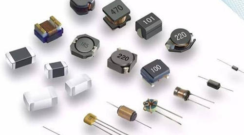
- Resistors (R): Current-limiting devices marked with resistance values or color codes.
- Capacitors (C): Energy-storage components with clear polarity markings on polarized types.
- Integrated Circuits (U/IC): Pin 1 is indicated by a dot or notch on the package.
- Diodes/Transistors (D/Q): Polarity and pin functions marked by bars or printed symbols.
How to Read PCB Silkscreen Markings and Labels?
Silkscreen labels display component designators, polarity, test points, and pin numbers to assist with assembly, testing, and diagnosis.
Silkscreen text matches reference designators in schematics and BOM documents.
Polarity indicators prevent reversed installation of sensitive components.
Test points (TP) are marked for debugging and electrical parameter measurement.
Connector pin labels ensure correct wiring and interface connections.
How to Trace Copper Traces and Signal Paths on a PCB?
Tracing circuits from the power input toward output sections helps you understand logical signal flow.
Begin at power connectors and follow traces to voltage regulators and main integrated circuits.
Use a multimeter in continuity mode to verify connections between components.
Differentiate power, ground, and signal traces by trace width.
Separate high-speed and low-speed paths to identify noise-reduction design principles.
How to Read Multilayer Circuit Boards and Inner Layers?
Multilayer PCBs use stacked layers for power, ground, and signal routing, connected by vias for compact layout.
Vias connect inner layers to surface traces for space-efficient routing.
Dedicated inner ground and power planes improve stability and reduce electromagnetic interference.
Blind and buried vias enable high-density miniaturized designs.
Layer stack-up labels specify the total layer count and the function of each layer.
What Tools Are Needed to Read a Circuit Board Accurately?
A digital multimeter, magnifier, schematic documentation, and anti-static tools ensure accurate and safe PCB analysis.
- Digital multimeter for continuity testing and voltage measurement.
- Magnifier or microscope for reading tiny SMD component markings.
- Schematic and BOM for cross-referencing physical and logical circuit design.
- Anti-static equipment to protect sensitive electronic components.
How to Read a Circuit Board Without a Schematic?
Locate power and ground, identify core ICs, map I/O connectors, and group components by function to infer circuit purpose.
First identify the main power input and voltage regulation section.
Locate key components such as microcontrollers, FPGAs, and interface chips.
Use connectors to determine input, output, and communication functions.
Group components into power, signal, control, and protection circuits.
How to Read Polarity Markings on PCB Components?
Polarity markings prevent component damage and circuit failure; common indicators include bars, dots, and flat edges.
- Electrolytic capacitors: a colored stripe marks the negative terminal.
- Diodes: a bar indicates the cathode side.
- Integrated circuits: a dot or notch shows the Pin 1 position.
- LEDs: a flat edge denotes the cathode pin.
How to Read a Circuit Board for Automotive Electronics?
Automotive PCBs are engineered for high-temperature resistance, vibration tolerance, and stable voltage performance.
Automotive BMS PCBs monitor battery cells in electric vehicles to ensure safe charging and discharging.
Engine control PCBs feature high-temperature layouts and anti-interference routing.
ADAS interface boards use shielded traces to protect sensor signals from interference.
We support on-demand customization and provide free DFM reports for automotive PCBs.
How to Read a Circuit Board for Industrial Control & Automation?
Industrial PCBs prioritize noise immunity, electrical isolation, and long-term reliability in harsh operating environments.
PLC I/O PCBs use isolated signal paths for factory automation equipment.
Motor drive PCBs use heavy copper traces for high-current handling and improved thermal management.
Sensor interface boards resist interference from industrial machinery and power systems.
How to Read a Circuit Board for Consumer Electronics & Communications?
Consumer and communication PCBs focus on miniaturization, high density, and RF signal integrity.
Smartphone mainboards use HDI design for compact component placement.
Router and base station PCBs maintain clean signal paths for stable wireless communication.
Wearable device PCBs use flexible or ultra-thin layouts for space efficiency.
FAQ: Frequently Asked Questions About Reading a Circuit Board
1. What do R, C, U, D, and Q mean on a circuit board?
R = resistor, C = capacitor, U = integrated circuit, D = diode, Q = transistor; these designators match schematic references.
2. How can I identify positive and negative terminals on PCB components?
Look for stripes, dots, or flat edges; capacitors and diodes have clearly marked polarities.
3. Why are some PCB traces wider than others?
Wider traces carry higher current levels, while narrow traces are used for low-power signal transmission.
4. What is the difference between a schematic and a physical PCB?
A schematic shows logical circuit connections, while a PCB displays physical layout and copper routing.
5. How do I locate ground (GND) on a circuit board?
Ground typically appears as large copper planes connected to mounting holes or power connector terminals.
6. Can I learn to read a circuit board without formal electronics training?
Basic PCB reading is achievable with this guide; advanced analysis requires fundamental circuit knowledge.
7. What common errors occur when reading a circuit board?
Missing polarity checks, blurred markings, and unrecognized test points often lead to misinterpretation.
8. How can I find broken or open traces on a PCB?
Use a multimeter in continuity mode to detect open circuits or cold solder joints.
9. What are vias and why are they used on PCBs?
Vias are conductive holes that connect layers in multilayer boards, enabling compact and efficient routing.
10. How do I correctly interpret high-frequency PCB layouts?
Focus on impedance control, matched trace lengths, and ground plane isolation for signal integrity.
11. What does “TP” stand for on a circuit board?
TP means test point, used for debugging, measurement, and quality inspection.
12. How can I distinguish power traces from signal traces?
Power traces are wider to carry higher current; signal traces are narrower and routed away from noise sources.
EBest PCB provides professional custom circuit board manufacturing for automotive electronics, industrial control, consumer electronics, and communications equipment. We support on-demand customization and offer free DFM reports to optimize your design for manufacturability and reliability. For inquiries or orders, contact us at sales@bestpcbs.com.