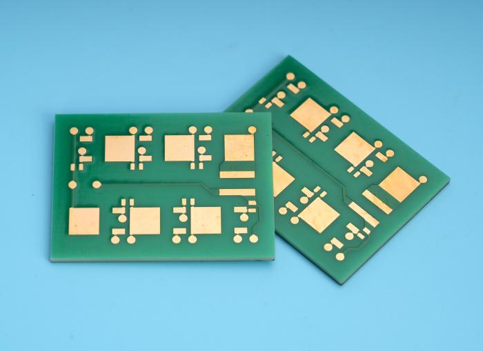
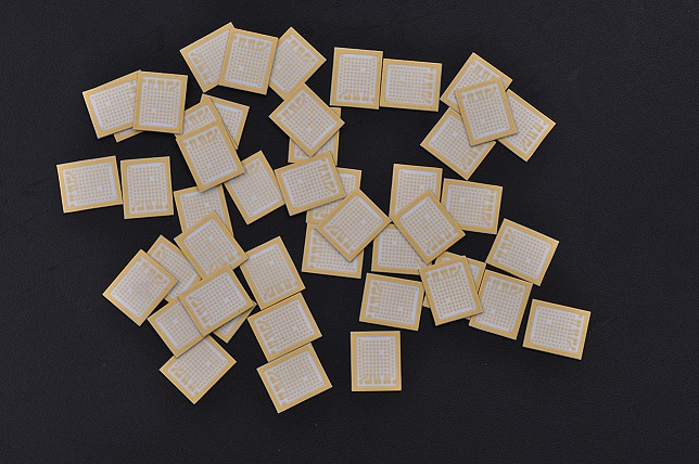
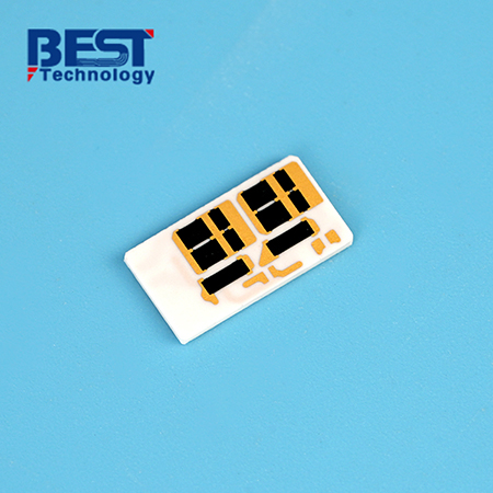
What is LTCC?
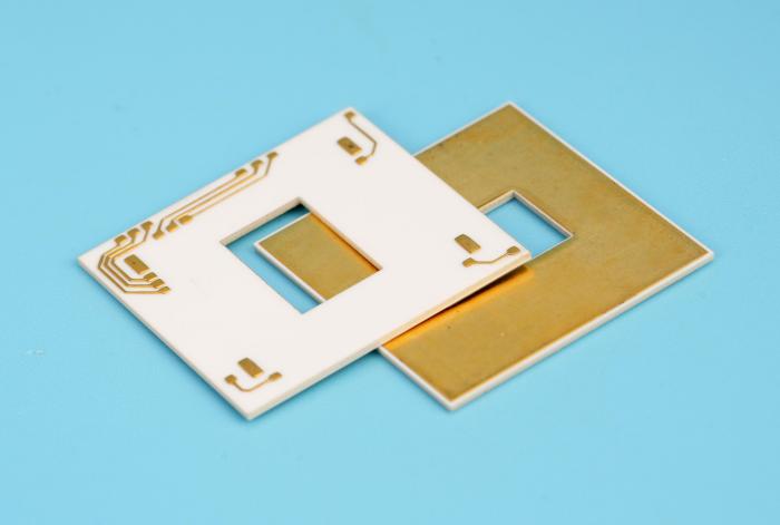
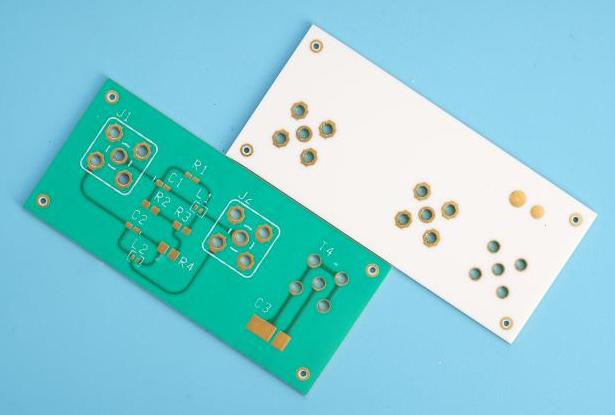
What is LTCC?LTCC low temperature cofired ceramic technology.What is the full name of LTCC?LTCC Ceramic PCB English full name Low temperature cofired ceramic, low temperature cofired ceramic technology is a multilayer circuit made by stacking unfired cast ceramic materials together, with printed interconnecting conductors, components, and circuits inside, and sintering the structure into an integrated ceramic multilayer material.

What are the advantages of LTCC?
- Green: LTCC technology uses materials and production processes that are more environmentally friendly, meeting the requirements of green manufacturing.
- Good compatibility: Compared with traditional high-temperature co-fired ceramic technology, LTCC is more compatible and can be adapted to more application scenarios.
- High production efficiency: LTCC technology has high production efficiency and can meet the needs of mass production.
- Low operating costs: LTCC technology has relatively low operating costs due to its productivity and compatibility advantages.
- High quality factor: In the RF microwave field, LTCC has the advantages of high quality factor, high stability, high integration, etc., which is suitable for high-performance electronic systems.
- Miniaturization and high density: LTCC technology can realize the miniaturization and high density of the circuit, which is conducive to the compact design and light weight of the system.
- Excellent electrical properties: LTCC material dielectric constant can be changed in a wide range, increasing the flexibility of circuit design, and at the same time has excellent high-frequency high-Q characteristics, the use of frequency can be as high as tens of GHz.
- High conductivity: the use of Ag, Cu and other metal materials with high conductivity as a conductor material, is conducive to improving the quality factor of the circuit system.
- Good temperature characteristics: good temperature characteristics, such as smaller coefficient of thermal expansion, smaller temperature coefficient of dielectric constant, etc., to ensure the stability and reliability of the circuit.
- High-temperature characteristics: can adapt to high current and high-temperature characteristics requirements, and has a better thermal conductivity than ordinary PCB circuit substrate, to improve the life and reliability of the circuit.
- Non-continuous production process: allows for inspection of raw substrates, improving yield and reducing costs.
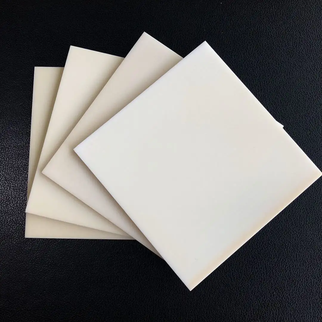
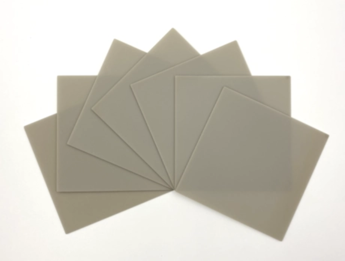
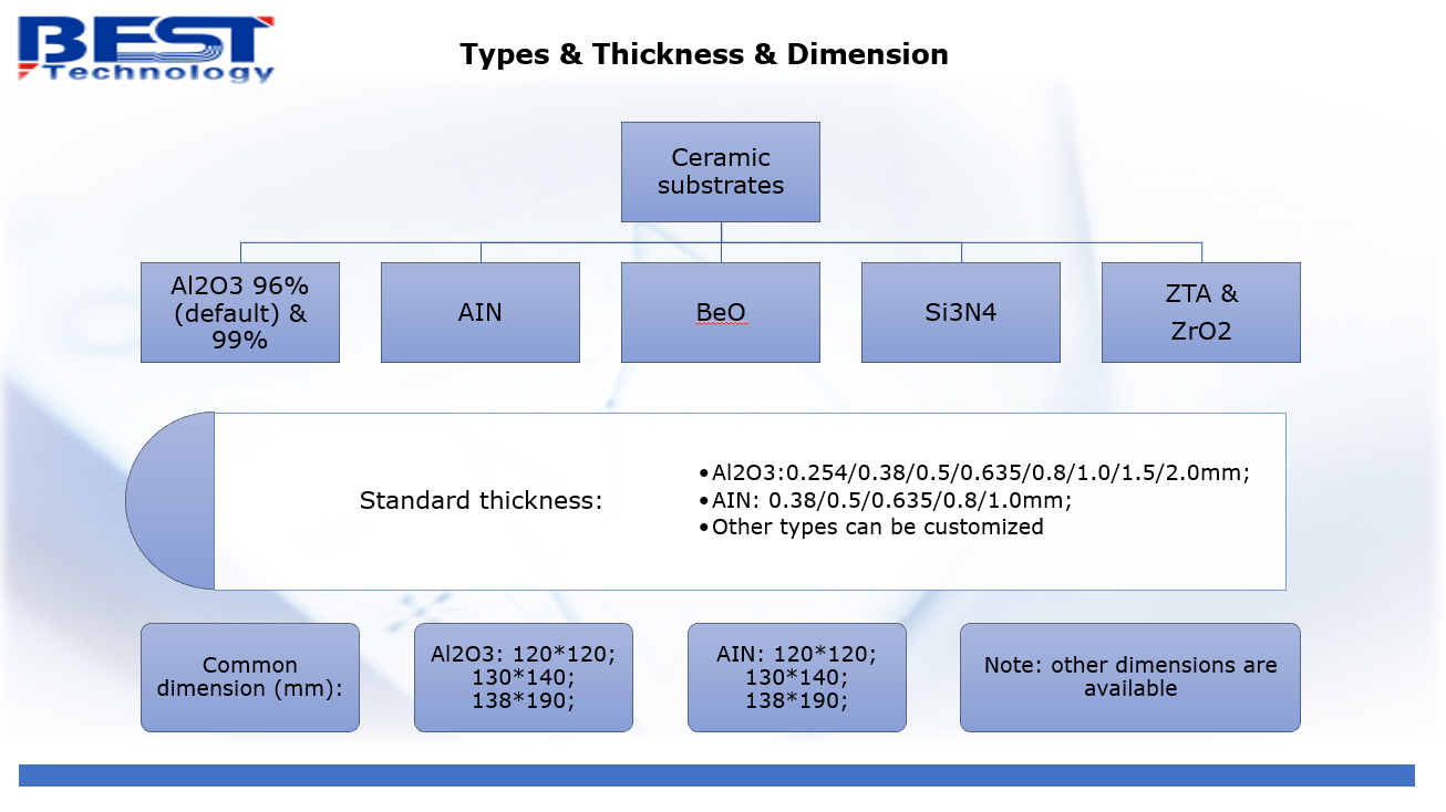
What are LTCC materials?
LTCC materials can basically be categorized into two main groups:
① Low dielectric constant materials (εr below 10), which are mainly used for passive integration, system level packaging and multilayer circuit substrates. In principle, the dielectric constant of such materials should be as low as possible to meet the requirements of high-speed signal transmission in the circuit; ② materials with medium to high dielectric constant, mainly used in passive integration, system-level packaging and multilayer circuit substrates.
② materials with medium-high dielectric constant (εr in 10 or more), mainly used to meet the special needs of various types of microwave devices.
From the material composition and structure division, the current low-temperature co-fired ceramic material system can be divided into three major categories: glass ceramics, ceramic-glass composites and glass bonded ceramics.
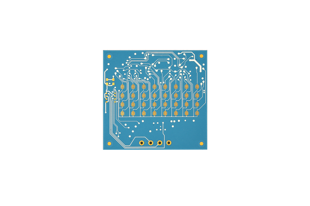
What is the LTCC process?
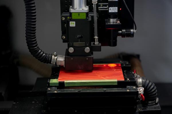
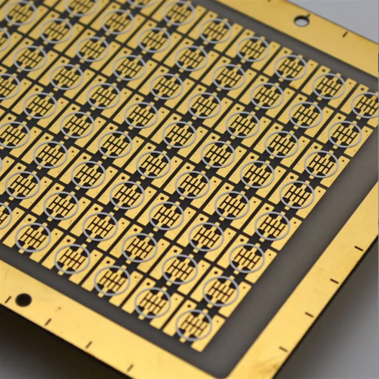
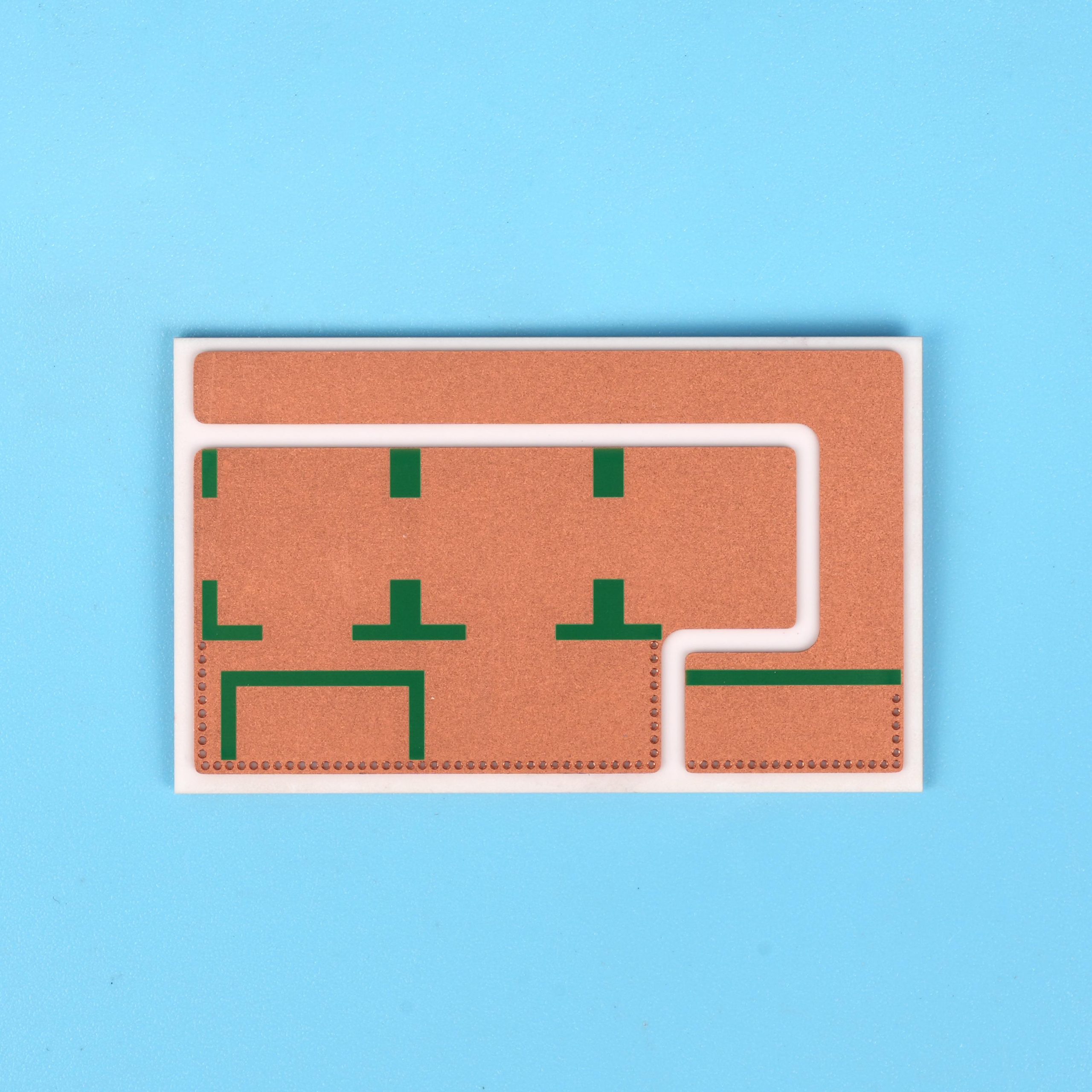
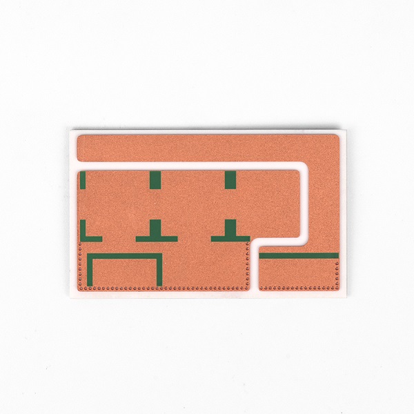
Cast:The purpose of casting is to transform ceramic powders into raw ceramic tapes for subsequent processing. A suitable binder is added to the ceramic powder, which is ball-milled and mixed to form a high-viscosity paste.
Perforation: perforation is a multilayer ceramic substrate manufacturing is extremely critical process technology, perforation hole size, location, precision, etc., directly affect the substrate internal alignment of the pass-through, wiring density, substrate quality and yield.
Fill holes: fill holes is the use of fill holes in the bottom of the machine airbag pressure will be masked filler plate filling paste extruded into the corresponding raw ceramic sheet through-hole, after drying, to complete the metallization process of raw ceramic.
Stacking and hot pressing: Stacking is printed raw porcelain in accordance with the design of the number and order of layers stacked together in a certain temperature and pressure, so that the raw porcelain tightly bonded to form a complete multi-layer substrate blanks.
Slicing: Slicing is to cut the raw porcelain blanks after lamination into raw porcelain blocks according to the design size requirements.
Co-firing: After lamination and slicing, the raw ceramic blocks are put onto the support in the sintering furnace, and sintered into qualified substrates under the appropriate curves and atmospheric conditions.
Inspection: Inspection is the basis for judging the quality of the substrate.
What is the firing temperature of LTCC?
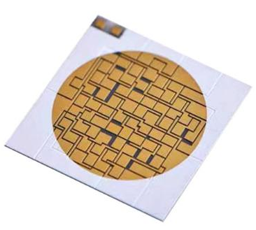
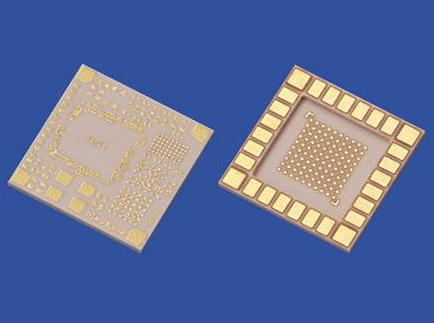
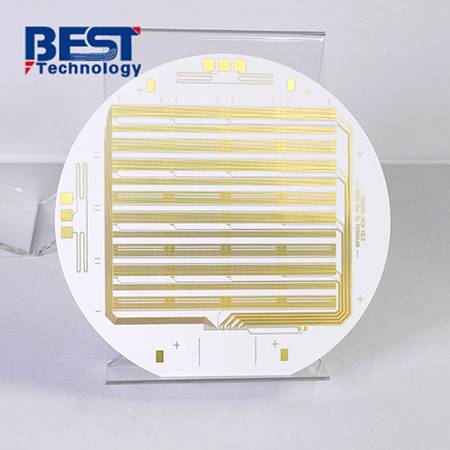
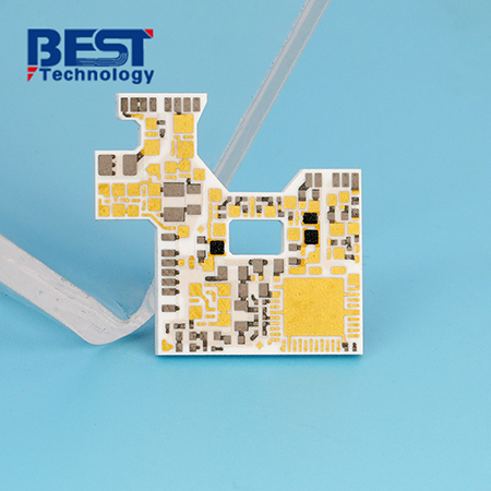
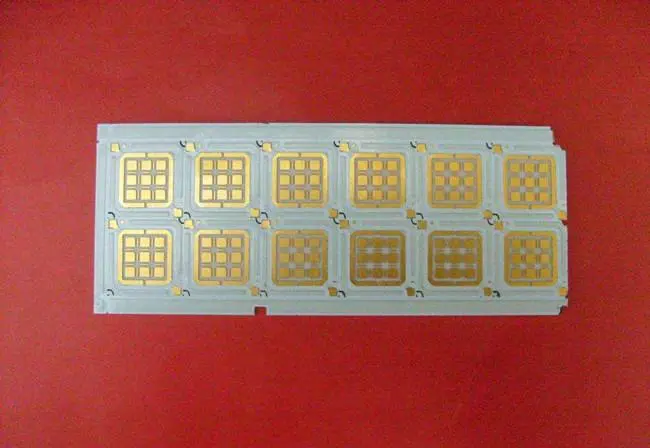
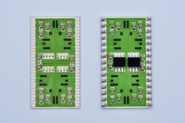
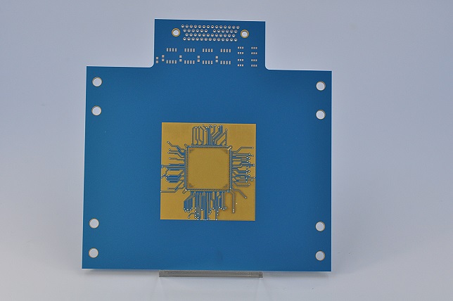
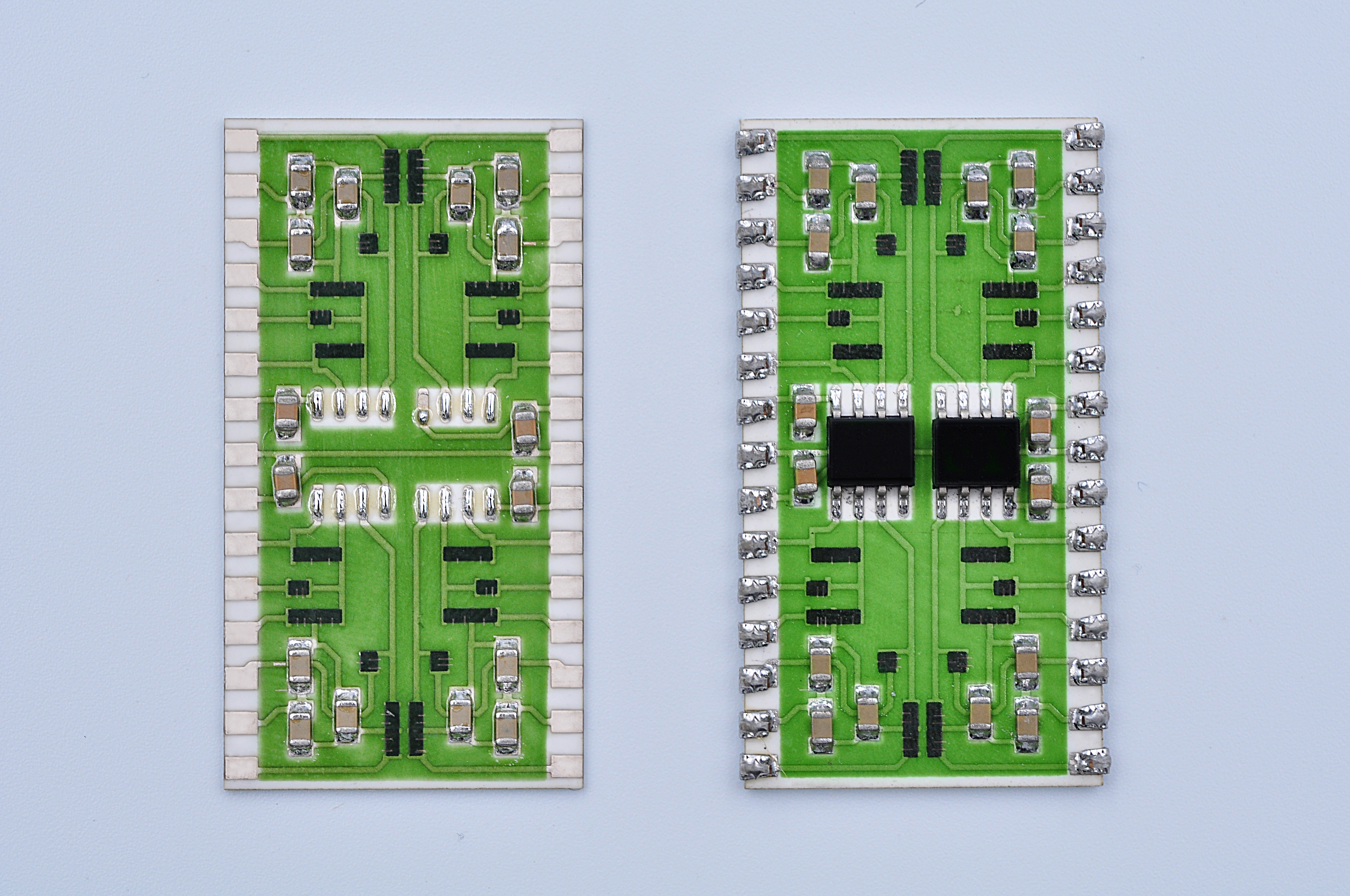
LTCC technology, or Low Temperature Co-Fired Ceramic Technology, is an advanced passive integrated and hybrid circuit packaging technology. This technology introduces a glass phase by adding a certain amount of glass powder to the ceramic slurry, allowing for a firing temperature that can be lower than 950°C. Specifically, the main feature of LTCC technology is the use of low-temperature (800°C~900°C) sintering materials and organic binder/incremental enhancers mixed in a certain ratio to generate raw ceramic wafers or raw embryo wafers by casting, followed by punching and laser punching, metallized wiring and through-hole metallization on the raw ceramic tape, followed by stacking, hot pressing, slicing, and gluing rows, and finally sintering at about 900°C to make multilayer Wiring substrate. This technology is easier to control during the sintering process and has a lower sintering temperature, which enables the realization of passive/active integrated functional modules, further miniaturizing the circuits and making them more dense, and is particularly suitable for components for high-frequency communication.
What is the difference between LTCC and HTCC?
Sintering Temperature: LTCC (Low Temperature Co-fired Ceramics) are generally sintered at temperatures between 800°C and 950°C, while HTCC (High Temperature Co-fired Ceramics) are sintered at temperatures between 1600°C and 1800°C. This difference in temperature directly affects the temperature of the components used. This temperature difference directly affects the choice of materials used and manufacturing process.
Materials Used: LTCC primarily uses metals with low melting points such as silver, gold, copper and palladium-silver, while HTCC uses metals with high melting points such as tungsten, molybdenum and manganese. In addition, LTCC uses dielectric materials such as glass-ceramics, ceramic-glass composites, and glass-bonded ceramics, while HTCC mainly uses high-temperature ceramic materials such as alumina and aluminum nitride.
Manufacturing process: The manufacturing processes of LTCC and HTCC are similar, both including the preparation of slurry, casting molding, drying of raw ceramic substrates, drilling of guide through holes, screen printing to fill the holes, screen printing lines, stacked sintering and other steps. However, the differences in firing temperatures and materials used result in different specific operations during the manufacturing process.
Areas of application: Due to LTCC’s lower sintering temperature and the use of low melting point metals, it is more suitable for high frequency circuits, RF modules, microwave circuits, and so on. HTCC, on the other hand, due to its higher sintering temperature and use of high melting point metals, is more suitable for high temperature, high power and high frequency applications such as power electronics, sensors and aerospace electronics.
What is the difference between LTCC and MLCC?
Materials: LTCCs use dielectric materials such as glass ceramics, ceramic-glass composites, and glass-bonded ceramics, while MLCCs use barium titanate (BaTiO3), titanium oxide (TiO2), calcium zirconate (CaZrO3), or other dielectric ceramic materials.
Sintering Temperature: LTCC is generally sintered between 800°C and 950°C, which is a low temperature sintering, while MLCC is generally sintered between 1100°C and 1350°C, which is a high temperature sintering.
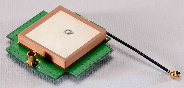
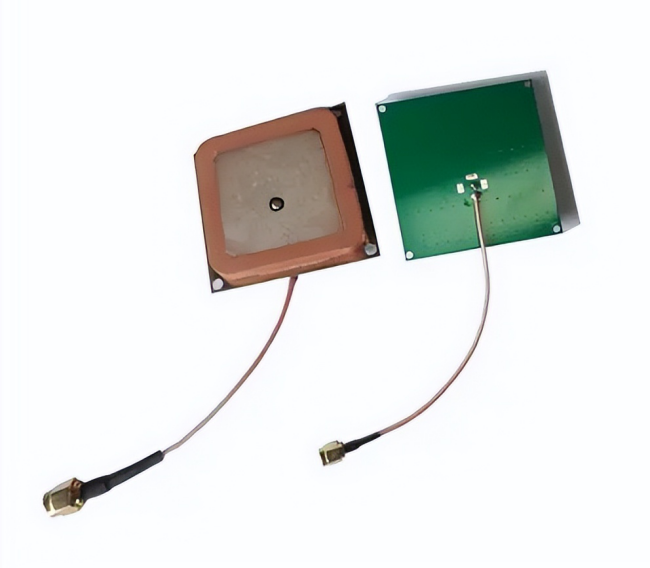
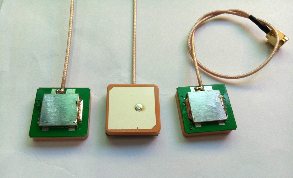
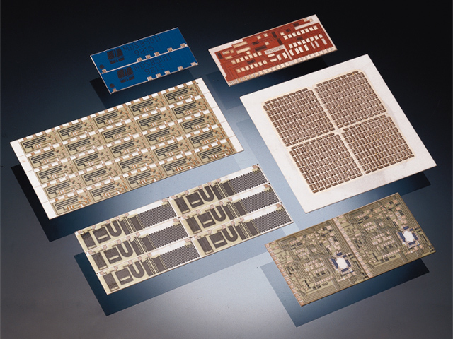
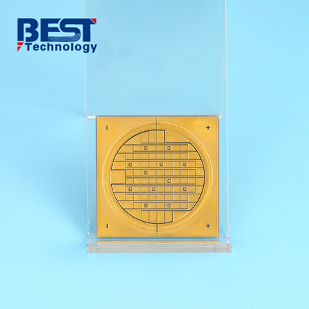
Product type: LTCC technology is mainly used for manufacturing filters, diplexers, couplers, baluns, antennas, ceramic substrates, ceramic package housings, etc., while MLCC is mainly used for capacitors.
Application areas: LTCC application areas are mainly focused on high frequency circuits, RF modules, microwave circuits and other areas that require high frequency characteristics; MLCC is widely used in consumer electronics, automotive electronics, communication equipment and many other areas.
Manufacturing process: LTCC’s manufacturing process involves laser drilling, microvia slurry injection, precision conductor paste printing, etc., which enables the integration of passive components; MLCC’s manufacturing process focuses on the basic construction and sintering process of multilayer ceramic capacitors.
Application of ltcc?
Communication field: LTCC technology is widely used in high-frequency communication components, especially in emerging fields such as 5G communication, Internet of Things, artificial intelligence, etc. Its high-density packaging technology can meet the demand for miniaturization and high-density of electronic components in these fields.
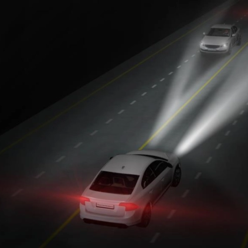
Automotive electronics: with the development of automotive electronics technology, the control system of modern automobiles depends more and more on electronic and information technology. LTCC technology can provide a high temperature, high humidity working environment to ensure the high reliability of the circuit system, so it has important applications in the field of automotive electronics.
Medical equipment: LTCC technology can greatly reduce the size of the three-dimensional structure of the circuit design, to adapt to the needs of medical equipment for miniaturization, high performance, and therefore has a wide range of applications in the field of medical equipment.
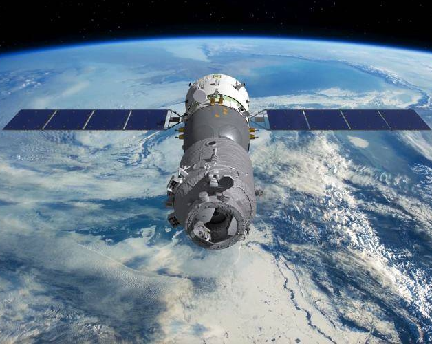
Aerospace: LTCC technology was first applied in aviation, aerospace and military electronic equipment, such as the development of satellite control circuit components, showing its reliability and high performance in extreme environments.