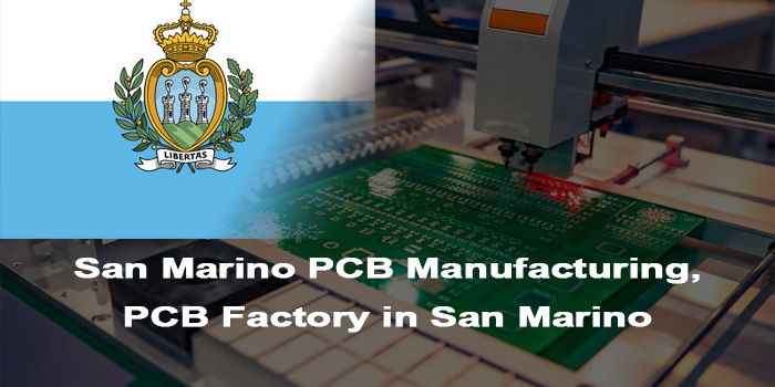
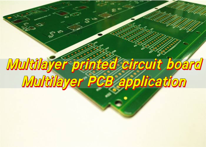
San Marino’s industrial sector relies heavily on small and medium-sized enterprises, with electronics being a key component. San Marino PCB manufacturingplays a vital role in supporting local electronic device production, from traditional machinery to emerging tech products. As a trusted San Marino PCB manufacturer, we understand the unique demands of the region’s market, delivering tailored services that align with local industrial characteristics. San Marino PCB manufacturing is not just about producing circuit boards; it’s about providing reliable support to keep local businesses competitive in the global electronics landscape.
Are You Facing These Problems of San Marino PCB Manufacturing?
Do you struggle with hidden design flaws that only emerge during production, leading to costly rework and delayed timelines for your San Marino PCB projects?
Is it challenging to find a PCB Factory in San Marino that offers fast prototyping without compromising on precision for urgent orders?
Are you dealing with inconsistent quality control in mass production, resulting in high defect rates for your PCB San Marino products?
Do you lack access to cost-effective solutions for complex designs, making your San Marino PCB manufacturing projects financially unsustainable?
Is coordinating the entire process from design validation to final delivery a hassle due to fragmented service providers in the San Marino PCB market?
Turnkey Solution from Requirement to Delivery
Free DFM Analysis: We conduct thorough design for manufacturing checks to identify and resolve potential flaws upfront, eliminating rework risks for your San Marino PCB projects.
Flexible Prototyping & Production: Our San Marino PCB plant offers 24-hour rapid prototyping and scalable mass production, balancing speed and precision for all order sizes.
Strict Quality Oversight: Full inspection for mass production and standardized quality control processes ensure consistent performance of every PCB San Marino product we deliver.
Cost-Optimized Solutions: We tailor cost-sensitive plans for complex designs, helping reduce overall expenses of your San Marino PCB manufacturing projects without quality trade-offs.
End-to-End Coordination: Our dedicated team manages the entire process, from design validation to logistics, simplifying your San Marino PCB project execution.
Why Choose EBest(Best Technology) for PCB Manufacturer in San Marino?
24-Hour Rapid Prototyping: Emergency orders are prioritized, with 24-hour turnaround for prototyping at our San Marino PCB factory.
19 Years of Expertise: Decades of experience in San Marino PCB manufacturing enable us to streamline processes and cut unnecessary costs.
Free DFM Analysis: Complimentary design validation to avoid production issues and optimize manufacturability of your San Marino PCB.
Global Certifications: Adherence to ISO9001:2015, ISO13485:2016, IATF16949, REACH and RoHS standards for compliant San Marino PCB products.
Competitive Pricing: We offer transparent, market-leading prices for San Marino PCB manufacturing with no hidden costs.
Cost-Sensitive Design Support: Our team optimizes designs to reduce material and production costs for your San Marino PCB projects.
Fast & Reliable Delivery: 99.2% order on-time delivery rate, ensuring your PCB San Marino projects stay on schedule.
Premium Quality Control: 100% full inspection for mass production and strict multi-stage QC processes to achieve ultra-low defect rates.
Customized Solutions: Tailored services for diverse industry needs, from standard to high-precision San Marino PCB manufacturing.
Types of San Marino PCB Manufacturing Services We Offer
We provide a full range ofSan Marino PCB manufacturing services, covering rapid prototyping, mass production, and specialized product lines. Our offerings include HDI PCBs for precision devices, multi-layer PCBs for complex circuit demands, rigid-flex PCBs for flexible installation scenarios, and high-frequency PCBs tailored for 5G and communication equipment. As a professional San Marino PCB company, we align our services with diverse industry application needs.
Our San Marino PCB manufacturing capabilities extend to handling intricate designs and strict performance standards across sectors. Every service integrates our core strengths of quality, speed and cost-efficiency, ensuring that both small-batch prototyping and large-scale production projects meet the highest reliability and compliance requirements for PCB San Marino clients.
Quality Certifications for San Marino PCB Manufacturing
ISO9001:2015: This quality management system standard integrates PDCA cycle and risk-based thinking, establishing a rigorous quality control framework for our San Marino PCB manufacturing processes to enhance customer satisfaction.
ISO13485:2016: Specifically designed for the medical device industry, it emphasizes regulatory compliance and full-life-cycle traceability, meeting the high safety requirements of medical-grade PCB San Marino products.
IATF16949: The automotive industry’s quality standard, ensuring our automotive-related San Marino PCB products can withstand extreme temperature cycles and mechanical vibrations with zero critical defects.
AS9100D: The top global quality standard for aerospace, exceeding general quality requirements to meet the high-reliability demands of aerospace-grade San Marino PCB manufacturing.
REACH: Complies with EU environmental regulations, restricting the use of hazardous substances in San Marino PCB products to ensure ecological safety.
RoHS: Prohibits harmful substances such as lead and mercury, ensuring our San Marino PCB products are environmentally friendly and compliant with global green production trends.
Project Background: An electronics company located in San Marino required high-precision multilayer PCBs for automotive-grade industrial control equipment. They had strict delivery time requirements and needed the PCBs to comply with the IATF16949 quality standard, which was a critical step in upgrading their production line.
Project Requirements: 12-layer PCBs, with a line width/spacing of 5mil (close to the industry limit of 4mil/4mil), 200 prototype samples + 5000 units for mass production, a total turnaround time of 15 days (including validation), and full compliance with the IATF16949 automotive quality system standard.
Project Challenges
The 5mil line width/spacing requirement demanded laser drilling accuracy of ±25μm, exceeding traditional PCB manufacturing capabilities.
The 15-day turnaround time was 40% shorter than the industry standard of 25 days for similar projects.
IATF16949 requires a CPK ≥ 1.33 (corresponding to a defect rate of 63 PPM), requiring zero critical defects.
Solution
We activated our 24-hour emergency prototype production line at our San Marino PCB factory, reducing prototype delivery time by 50%.
We employed UV laser drilling technology (accuracy ±10μm) to achieve stable 5mil line width/spacing.
We implemented a three-stage AI-driven inspection process (AOI + X-ray + electrical testing), achieving a defect detection rate of 99.8%.
We conducted free DFM analysis, optimizing 8 design points and improving manufacturability by 32%.
Results
Prototype samples were delivered within 22 hours (12% ahead of the promised 24 hours); mass production was completed 2 days ahead of schedule, shortening the total cycle by 13%. The final defect rate was 0.03% (300 PPM), far below the IATF16949 requirement of 63 PPM. The customer’s equipment successfully passed 500 hours of high-temperature cycle testing, and we secured a three-year long-term contract for the customer’s San Marino PCB manufacturing needs.
How to Get A Quote for Your San Marino PCB Manufacturing?
To obtain a PCB production quote, follow these structured steps:
Compile essential design files including Gerber, Bill of Materials (BOM), and mechanical drawings. Ensure files are in universal formats compatible with manufacturing standards.
Define physical parameters: board dimensions, layer count, and copper weight. These directly influence material usage and production complexity.
Select material specifications: choose between standard FR-4 or specialized substrates like high-frequency laminates. Specify surface finishes such as ENIG, HASL, or immersion silver based on application needs.
Confirm order quantity and delivery urgency. Higher volumes often reduce per-unit costs, while expedited timelines may require premium pricing.
Submit all specifications through an online quoting platform or interface. Provide detailed parameters without omitting critical data to ensure accurate pricing.
Compare quotes from multiple sources by evaluating turnaround time, quality certifications, and cost breakdowns. Prioritize suppliers with transparent communication and technical compliance.
Welcome to contact us if you have any request for San Marino PCB manufacturing: sales@bestpcbs.com.
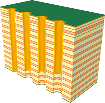
Multilayer printed circuit board is a circuit board built from three or more conductive copper layers laminated together with insulating material. Unlike single- or double-sided boards, multilayer PCBs stack internal signal and power layers between outer layers, allowing complex circuits to fit into a much smaller footprint.
What is a multilayer PCB?
Multilayer printed circuit board is a circuit structure that combines three or more conductive copper layers into a single, unified board. These layers are separated by insulating materials and bonded together under heat and pressure to form a compact electrical platform.
In practical electronics, a multilayer printed circuit board allows designers to place signal layers, power planes, and ground planes in carefully controlled positions. This internal structure improves electrical stability while reducing electromagnetic interference.
As products continue to shrink while performance expectations rise, multilayer printed circuit boards have become the backbone of modern electronic systems. Smartphones, medical equipment, automotive electronics, and industrial controls all rely on this technology to meet demanding requirements.
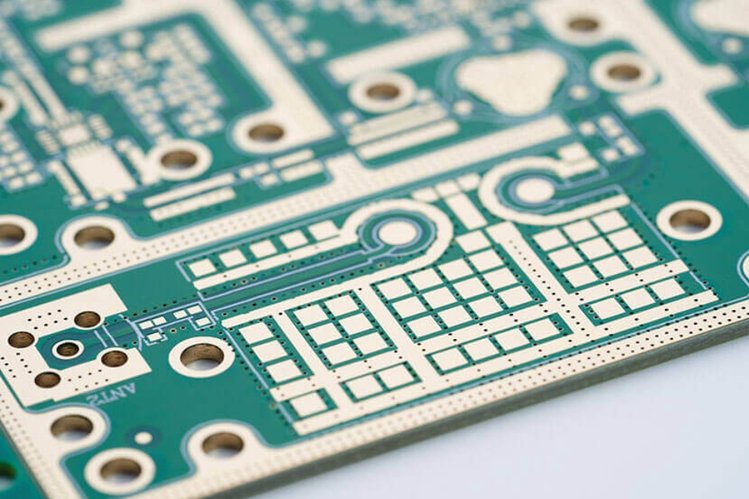
From a manufacturing standpoint, multilayer PCB production requires precise process control. Layer alignment, dielectric thickness, copper balance, and via reliability all influence final performance. At EBest Circuit (Best Technology), multilayer printed circuit boards are produced as part of a fully integrated Turnkey EMS service, ensuring design intent and production reality stay aligned.
How to identify multi-layer PCB?
Identifying a multi-layer PCB usually starts with visual inspection, but surface clues alone are often not enough. Unlike single-layer boards, multilayer designs hide most of their complexity inside the board structure.
One common indicator is the presence of plated through holes that connect multiple layers. These vias typically appear filled or copper-lined, suggesting internal interconnections. Dense via fields are often associated with multilayer printed circuit boards, especially in high-speed or high-density designs.
Board thickness can also provide hints. Multilayer PCBs are often thicker than simple boards, even when designed for compact products. The additional dielectric layers add measurable depth.
For accurate identification, manufacturers use cross-sectional analysis or fabrication drawings. These clearly show the number of copper layers and their arrangement. It is defined, documented, and verified before production begins.
How can you tell how many layers a PCB has?
Determining the exact number of layers in a PCB requires more than observation. The most reliable method is reviewing the fabrication documentation, where the stack-up is clearly specified. This document lists each copper layer, dielectric material, and thickness in sequence.
In a production environment, cross-section testing is commonly used. A small sample of the board is cut and polished so the internal layers can be counted under magnification. This method is precise and often used for quality validation in multilayer PCB manufacturing.
Electrical testing can also provide indirect clues. The number of reference planes affects impedance behavior and signal integrity. Experienced engineers can infer layer complexity based on performance characteristics, but this approach is supplementary rather than definitive.
For customers working with Turnkey EMS providers like EBest Circuit (Best Technology), layer count transparency is standard practice. Every multilayer printed circuit board process begins with a confirmed stack-up, ensuring consistency from prototype to volume production.
What material is used for multilayer PCB?
The most common material used in multilayer printed circuit boards is FR-4, a glass-reinforced epoxy laminate. FR-4 offers a balance of mechanical strength, electrical stability, and cost efficiency.
For more demanding environments, alternative materials are often selected. High-Tg laminates improve thermal performance and dimensional stability. Low-loss materials support high-speed signal transmission by reducing dielectric losses.
Copper foil is used for conductive layers, with thickness selected based on current requirements and impedance design. The dielectric layers between copper planes control capacitance, signal propagation, and thermal behavior. Material selection directly influences power bus decoupling on multilayer printed circuit boards, especially in high-current designs.
How to design a multilayer PCB?
Designing a multilayer PCB begins with system requirements, not routing convenience. Engineers first define signal integrity goals, power distribution needs, and thermal constraints.
A well-designed multilayer printed circuit board separates functions across layers. Signal layers are placed adjacent to solid reference planes. Power planes are distributed to minimize voltage drop and noise.
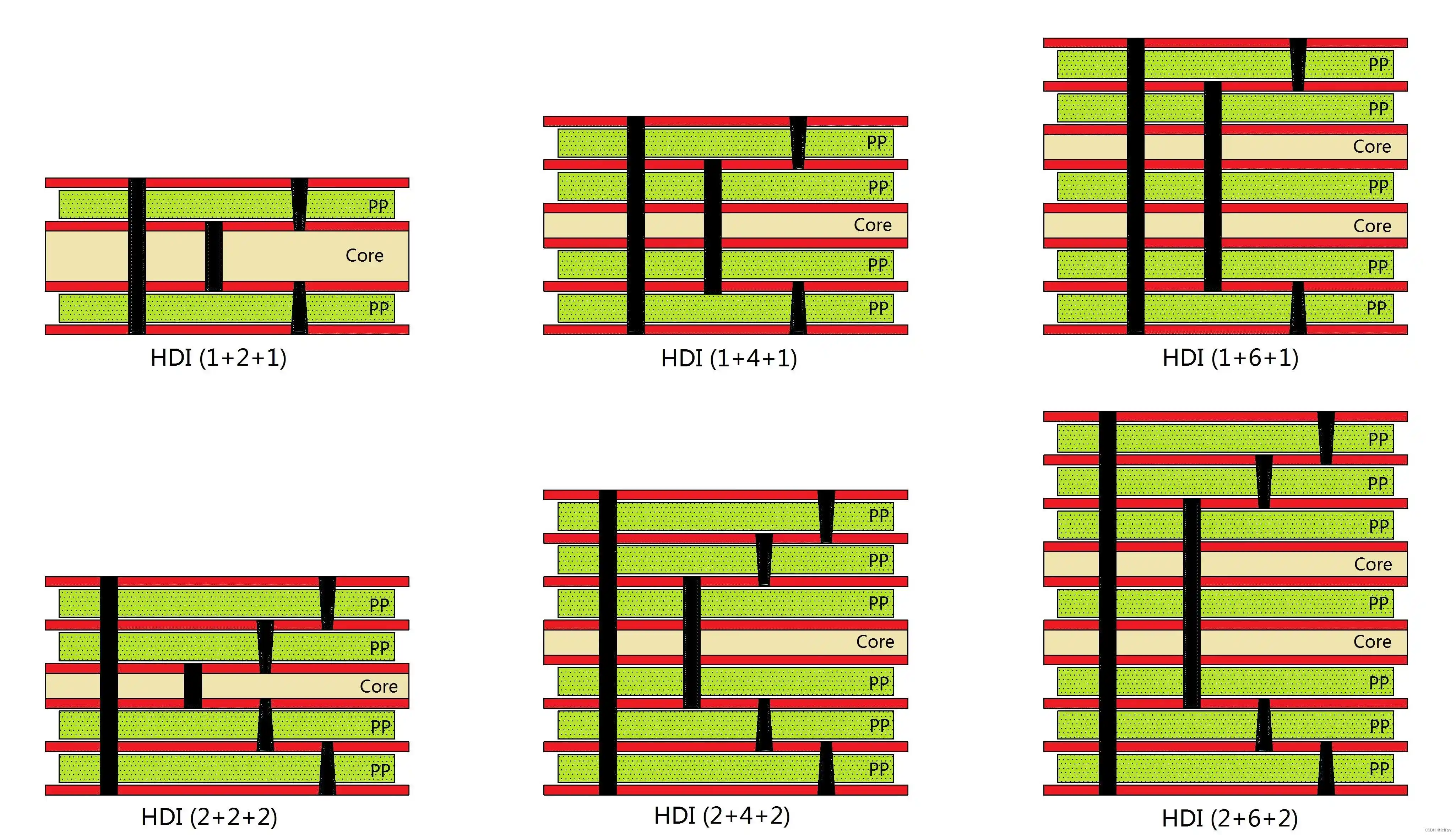
Via strategy is another critical element. Through vias, blind vias, and buried vias each serve different purposes. High-speed signal optimization at differential vias in multilayer printed circuit boards requires careful geometry control to maintain impedance and timing balance.
Simulation plays an important role in modern design. Analytical evaluation of via plate capacitance for multilayer printed circuit boards and packages helps engineers predict parasitic effects before fabrication.
At EBest Circuit (Best Technology), design support is closely tied to manufacturing expertise. Design-for-manufacturability reviews ensure that multilayer PCB designs translate smoothly into reliable production, even for complex stack-ups.
What is the highest number of layers in a PCB?
There is no absolute limit to the number of layers in a PCB, but practical constraints define realistic boundaries. Commercial multilayer printed circuit boards commonly range from four to twenty layers. Advanced systems may use thirty or more layers when required.
In high-performance computing and aerospace applications, extremely high layer counts have been achieved. These designs demand precise control of materials, lamination cycles, and registration accuracy. Each added layer increases complexity and cost.
More layers provide routing flexibility and power integrity, but they also introduce manufacturing challenges. Balance is essential.
Experienced manufacturers guide customers toward optimal solutions rather than maximum complexity. The goal is not to use the most layers, but the right number of layers to meet performance and reliability goals.
What is the purpose of having multiple layers in a PCB?
The primary purpose of multiple layers in a PCB is functional separation. Different electrical roles are assigned to dedicated layers, improving performance and predictability. Signal layers carry data. Power layers distribute energy. Ground layers provide stable references.
This separation enhances signal integrity by reducing noise coupling and crosstalk. It also supports efficient power distribution, which is critical in modern electronics with fast switching devices.
Multilayer printed circuit boards also enable compact product design. By routing signals vertically through vias, designers reduce board area while maintaining functionality.
Thermal performance is another key benefit. Internal copper planes act as heat spreaders, helping manage temperature rise. When designed correctly, multilayer structures contribute directly to long-term reliability.
What are the advantages of multilayer PCBs?
Multilayer PCBs offer several compelling advantages that make them the preferred choice for advanced electronics.
One major benefit is improved electrical performance. Shorter signal paths and controlled impedance support high-speed operation.
Another advantage is mechanical stability. Laminated layers create a rigid structure that resists warping and vibration.
Design flexibility also increases with layer count. Engineers can route complex circuits without overcrowding, improving yield and manufacturability.
From a system perspective, multilayer printed circuit boards enable integration. More functionality fits into less space, reducing assembly complexity.
How do multilayer PCBs work?
Multilayer PCBs work by distributing electrical functions across stacked conductive layers. Signals travel through copper traces on designated layers, while power and ground planes provide stable electrical environments.
Vias connect these layers vertically, creating three-dimensional routing paths. This structure allows complex interconnections without excessive surface congestion.
The internal planes also act as capacitive elements. Power bus decoupling on multilayer printed circuit boards benefits from closely spaced power and ground layers.
Manufacturing precision ensures that each layer aligns correctly. Lamination bonds layers into a single unit, while drilling and plating create reliable interconnections. The result is a cohesive electrical platform designed to perform consistently.
What is the difference between single layer and multilayer PCB?
The difference between single layer and multilayer PCB lies in complexity, capability, and application scope. A single-layer board has one conductive layer and is suitable for simple circuits. It offers low cost and straightforward manufacturing.
A multilayer PCB, by contrast, supports complex routing and higher performance. Multiple layers enable better signal control, power distribution, and noise reduction.
Single-layer boards struggle with high-speed signals and dense layouts. Multilayer printed circuit boards handle these challenges with structured stack-ups and dedicated planes.
The choice depends on requirements. Simple products benefit from simplicity. Advanced systems demand multilayer solutions.
Common multilayer PCB application scenarios
Multilayer PCB application spans nearly every advanced electronic sector.
Consumer electronics rely on multilayer printed circuit boards to support compact, feature-rich devices. Smartphones and tablets are prime examples.
In medical electronics, multilayer designs support precision, reliability, and miniaturization. Diagnostic equipment and monitoring systems depend on stable signal integrity and controlled power distribution.
Automotive systems use multilayer PCBs for safety-critical functions. Engine control units, driver assistance systems, and infotainment platforms all benefit from multilayer architecture.
Industrial equipment also relies heavily on multilayer PCB application. Automation, robotics, and power control systems require robust designs that withstand harsh environments.
Across all these scenarios, manufacturing consistency matters. EBest Circuit (Best Technology) integrates multilayer PCB manufacturing with assembly and testing, delivering complete Turnkey EMS solutions that support diverse applications.
Conclusion:
Multilayer printed circuit boards form the foundation of modern electronics. They enable compact design, stable performance, and functional integration across industries. From material selection to stack-up design, every decision shapes reliability and efficiency.
Choosing the right partner is just as important as choosing the right layer count. If you are planning a multilayer PCB project or need full Turnkey EMS support, EBest Circuit (Best Technology) is ready to help.
Medical PCB assemblies are the critical, intelligent core of modern medical electronics, enabling everything from patient monitoring to life-saving therapeutic interventions. This article provides a comprehensive guide to navigating the unique challenges of sourcing and manufacturing reliable, compliant, and scalable medical PCB assemblies with the speed demanded by today’s healthcare innovation cycles.
Medical device development teams often face a unique mix of regulatory, reliability, and time-to-market pressures that standard PCB suppliers are not equipped to handle.
Heavy compliance burden: ISO 13485, FDA QSR, and IEC 60601 add time and complexity to PCB assembly for medical projects.
Zero tolerance for defects: Any assembly error risks device failure, recalls, and patient safety.
Prototype-to-production gap: Few suppliers support both fast PCB prototype assembly and scalable medical PCB assembly services.
Cost vs reliability conflict: Cheap medical PCB assembly options often undermine long-term quality.
Long lead times: Complex multilayer or rigid-flex PCB assembly delays validation and launch schedules.
A medical-focused manufacturer addresses these issues through systems, processes, and infrastructure designed specifically for regulated medical electronics.
Built-in compliance: ISO 13485 quality systems embedded across all operations.
Controlled manufacturing: SPC, AOI, and X-ray inspection ensure high-reliability medical PCB assembly.
Scalable workflows: Quick turn medical PCB assembly using the same processes as volume production.
Cost control by design: DFM-driven sourcing without compromising medical device PCB assembly integrity.
Rapid delivery: Dedicated lines and medical devices PCB assembly in stock for fast turnaround.
At EBest Circuit (Best Technology), we specialize in overcoming these exact challenges. With two decades of focused expertise, we provide end-to-end medical PCB assembly services that blend stringent quality control with remarkable agility. Our facility is purpose-built to deliver scalable medical PCB assemblies with quick delivery, ensuring your innovations move swiftly from concept to clinic. Pls feel free to contact us at sales@bestpcbs.com to start a conversation about your PCB assembly for medical project.
What Are Medical PCB Assemblies Used for in Medical and Healthcare Electronics?
Medical PCB assemblies are the fundamental building blocks that bring intelligence and functionality to healthcare technology. They are found in any device that diagnoses, monitors, or treats a patient, requiring exceptional reliability and precision.
Diagnostic Equipment: Imaging systems (MRI, CT, ultrasound), blood analyzers, and glucose monitors.
Therapeutic Devices: Infusion pumps, ventilators, cardiac defibrillators, and neuromodulators.
Laboratory & Surgical Tools: DNA sequencers, automated lab equipment, and robotic surgical arms.
In summary, medical PCB board assembly is ubiquitous in modern medicine, forming the reliable electronic foundation for devices that improve and save lives.
What Makes Medical PCB Assembly Different From Standard PCB Assembly?
Medical PCB assembly operates under a fundamentally different set of expectations, where compliance, traceability, and risk control are integral to every production step rather than optional quality enhancements.
Aspect
Standard PCB Assembly
Medical PCB Assembly
Quality Standards
ISO 9001
ISO 13485, ISO 14971
Reliability Focus
Functional performance
High-reliability, lifecycle-driven
Cleanliness Control
Basic flux removal
Ultrasonic cleaning, ionic testing
Testing & Inspection
Visual + electrical
AOI, X-ray, ICT, functional test
Documentation
Assembly records
Full DHR, lot traceability
In essence, the distinction is not limited to added inspections or certifications; medical PCB assembly reflects a system-level commitment to validated processes, documented risk management, and complete traceability—principles that exist to protect patients, not just products.
What Are the Key Process Controls in Medical PCB Assembly?
Compliance is non-negotiable. Key standards include:
ISO 13485: The international standard for Quality Management Systems specific to medical devices.
FDA 21 CFR Part 820 (QSR): The US Food and Drug Administration’s Quality System Regulation.
IEC 60601-1: The safety standard for medical electrical equipment.
To meet these, rigorous process controls are implemented:
Compliant Material Management: Use of certified, long-lifecycle components from approved vendors; strict moisture-sensitive device (MSD) handling.
Comprehensive Inspection: AOI for surface defects, X-Ray for BGA and via integrity, and high-magnification visual inspection.
Cleaning & Contamination Control: Validated cleaning processes to achieve low ionic contamination levels per IPC-5701.
Full Traceability: Barcode tracking of PCBs and components throughout assembly, linking all process data to each unique serial number.
Adherence to these requirements and controls transforms a standard PCB assembly into a certified, reliable medical PCB assembly.
What Design Challenges Commonly Affect High-Reliability Medical PCB Assembly?
Design for Manufacturing (DFM) and Design for Reliability (DFR) are critical. Common challenges include:
Miniaturization & High Density: Packaging complex functionality into small, wearable, or implantable devices requires advanced rigid-flex PCB assembly and microvia technology.
Signal Integrity: Isolating sensitive analog signals (e.g., ECG, EEG) from digital noise in mixed-signal designs.
Thermal Management: Efficiently dissipating heat in sealed, compact enclosures to ensure component longevity.
Power Integrity: Ensuring stable, clean power delivery to sensitive analog and RF circuits.
Long-Term Reliability: Designing for 10-15+ year lifespans, considering factors like thermal cycling, mechanical stress, and conformal coating compatibility.
Proactive collaboration with your medical PCB assembly manufacturer during the design phase is essential to mitigate these challenges and ensure a manufacturable, reliable product.
When Do OEMs Need Quick Turn Medical PCB Assembly During Product Development?
Speed is crucial in medical device development without sacrificing compliance. Quick turn medical PCB assembly is vital during:
Concept Validation: Building initial functional prototypes to test core ideas.
Design Iterations: Rapidly incorporating design changes and testing new versions.
Clinical Trial Units: Producing small batches of fully compliant devices for pilot studies or regulatory submissions.
Pre-Production Runs: Finalizing manufacturing processes before committing to full-scale volume.
Urgent Design Changes: Addressing issues found in verification testing or preparing for a derivative product.
A partner offering fast PCB prototype assembly supplier for medical devices capabilities within a quality framework accelerates innovation and reduces time-to-market.
Why Do Buyers Choose a China Medical PCB Assembly Manufacturer for Medical Projects?
Buyers choose a China medical PCB assembly manufacturer when they need a practical combination of medical-grade capability, scalable capacity, and disciplined cost control—without sacrificing the process rigor required for regulated products.
1) Mature, Scalable Manufacturing Capacity for NPI and Volume
The first driver is throughput and repeatability. Many medical programs must move from prototypes to pilot builds, then into stable volume—often with unpredictable ramp curves.
Flexible capacity planning: China-based EMS ecosystems commonly support quick pivots between prototype, pre-production, and volume.
High-mix, high-volume experience: Facilities are typically set up to run diverse SKUs while maintaining stable yield.
Parallel production resources: The ability to run multiple lines (SMT + THT + test) shortens bottlenecks during ramp-up.
Fundamentally, medical programs rarely fail because of “design only”; they fail when production cannot scale cleanly with consistent quality.
2) Strong Cost-Performance Ratio Without “Cheapening” the Build
Serious buyers are not chasing the lowest quote; they are optimizing total landed cost (cost + yield + rework + delays + compliance overhead).
Lower conversion cost at scale: Labor, factory overhead, and supply chain leverage often reduce assembly cost per unit.
Better cost control through DFM: Many manufacturers run strong manufacturability review loops to prevent rework drivers (fine-pitch bridging, voiding risk, poor stencil strategy).
Purchasing power on standard parts: Larger BOM volumes can translate into better pricing, lead-time priority, and alternative sourcing options.
When a supplier can improve first-pass yield and reduce rework, the “cheapest” build is often the one with the fewest surprises—not the lowest line-item price.
3) Deep Supplier Ecosystem and Faster Component Procurement Options
China’s electronics manufacturing clusters provide dense upstream support that can reduce procurement friction.
Broader sourcing channels: Easier access to alternates, second sources, and regionally stocked inventory.
Faster response to shortages: Buyers often benefit from quicker substitutions when parts go EOL or go on allocation.
Integrated services nearby: Stencil houses, tooling, test fixture shops, conformal coating, cable harness, and box build are frequently close to the assembly site.
In medical device timelines, procurement delays can be as damaging as engineering delays.
4) Increasing Availability of Medical-Grade Systems and Traceability
For medical projects, the deciding factor is not geography—it is whether the system can withstand audits and sustain compliance.
ISO 13485 capability is more common than before: Many suppliers have built medical-focused QMS frameworks to compete globally.
Traceability infrastructure: Lot tracking for components, solder paste, process parameters, and test records is now a baseline expectation.
Documentation discipline: Buyers often require records that support DHR-style documentation packages and controlled revision management.
If the supplier can prove traceability, process control, and change management, the risk profile becomes manageable.
5) Process Technology and Inspection Tooling That Matches Medical Complexity
Medical electronics frequently includes miniaturization, mixed-technology assembly, and reliability-critical soldering—areas where process technology matters.
Advanced inspection coverage: AOI and X-ray are often standard for fine-pitch, QFN/QFP, and BGA-heavy builds.
Process controls for consistency: Controlled reflow profiling, SPI (where available), and defined workmanship criteria reduce variability.
Test readiness: Many manufacturers can support ICT/flying probe strategies and functional test setup when the program is properly planned.
Better detection earlier in the process reduces escapes, field failures, and costly investigation loops.
6) Program Management and Turnaround Speed for Competitive Time-to-Market
Medical teams frequently operate on compressed schedules—design iteration, verification builds, clinical timelines, and launch windows.
Shorter build cycles for iteration: Faster feedback loops between engineering and manufacturing accelerate design stabilization.
More responsive engineering support: DFM feedback, stencil optimization, and assembly process suggestions can arrive quickly when systems are mature.
Coordinated NPI ramp: A capable partner can keep the same process discipline from prototype through production.
Time-to-market is a cost. A delay in validation or launch is often more expensive than a small delta in per-unit assembly price.
7) What Smart Buyers Check Before They Commit
To ensure the value proposition is real, experienced buyers validate capability with objective checkpoints:
Certifications: ISO 13485 (and ISO 9001 as baseline); confirm scope and validity.
Traceability depth: Component lot, process parameter, inspection/test record linkage.
Inspection and test coverage: AOI/X-ray strategy, acceptance criteria, and defect escape controls.
Change control: ECO process, AVL control, and substitution approval workflows.
Medical program references: Evidence of sustained quality on regulated products.
All things considered, buyers choose a China medical PCB assembly manufacturer because the best-qualified providers combine scalable capacity, cost discipline, and increasingly mature medical-grade quality systems—a mix that supports both aggressive timelines and stringent reliability expectations.
Top 10 Medical PCB Assembly Supplier in China
While many claim expertise, the leaders distinguish themselves through:
Certified Medical Focus (ISO 13485, FDA registered)
For regulated medical devices, buyers should validate ISO 13485 scope, traceability depth, and audit readiness rather than relying on scale alone.
What Capabilities Define Reliable Medical PCB Assembly Factories?
For medical electronics, reliability is paramount. EBest Circuit (Best Technology) demonstrates its capability as a qualified medical PCB assembly partner through a commitment to stringent quality standards, advanced manufacturing precision, and comprehensive control over the entire production process.
EBest Circuit establishes reliability on a foundation of advanced technical capabilities, enabling the production of complex PCBs for applications ranging from patient monitors to advanced imaging systems.
High-Density Interconnect (HDI) & Miniaturization: EBest Circuit (Best Technology) excels in HDI processes, capable of producing laser-drilled micro-vias as small as 0.10mm (4 mil) and conductor traces/spaces down to 0.075mm (3mil), which is critical for miniaturized medical implants and portable devices.
Advanced Layer & Material Expertise: The company manufactures complex multilayer boards (up to 50 layers routinely) and is proficient with a wide range of materials, including high-frequency/RF boards (Rogers, Taconic), Metal Core PCBs (MCPCBs) for thermal management, and heavy copper boards (up to 20 oz inner layer) for high-current applications.
Stringent Tolerances: EBest Circuit (Best Technology) maintains tight controls, such as a hole position tolerance of ±0.05mm and impedance control within ±5Ω (<50Ω) or ±10% (≥50Ω), ensuring signal integrity and manufacturing consistency essential for medical devices.
2. Quality Assurance, Certifications, and Testing Regime
EBest Circuit (Best Technology)’s commitment to quality is validated by relevant certifications and a robust, in-house inspection infrastructure.
Medical-Specific Certifications: EBest Circuit (Best Technology) holds ISO 13485:2016 certification, the quality management standard specific to medical devices, alongside IATF 16949 and ISO 9001:2015.
Comprehensive In-House Testing: The company operates an effective failure analysis lab equipped with advanced tools, including 3D Automated Optical Inspection (AOI), X-Ray Inspection (AXI) for BGAs, flying probe testers for electrical verification, and micro-section analysis for validating internal layer integrity.
Regulatory Compliance: EBest Circuit (Best Technology) ensures compliance with RoHS and REACH directives, guaranteeing that materials meet environmental and safety standards.
3. Controlled Environments and Full Turnkey Service
EBest Circuit (Best Technology) provides end-to-end control and security, which is crucial for medical device manufacturing.
Supply Chain Control: Through its full turnkey service model, EBest Circuit (Best Technology) manages component sourcing from authorized distributors to avoid counterfeit parts, ensuring full traceability—a critical regulatory requirement.
End-to-End Integration: By managing everything from PCB fabrication and component procurement to assembly and final box-build, EBest Circuit (Best Technology) simplifies the supply chain, reduces lead times, and maintains single-source accountability.
4. Specialized Engineering Expertise
EBest Circuit (Best Technology) supports its clients with a team of engineers experienced in the regulatory and technical demands of medical device electronics. This expertise encompasses design for manufacturability (DFM) and a focus on creating reliable, manufacturable products from the initial design stage.
In summary, EBest Circuit (Best Technology) positions itself as a reliable medical PCB assembly partner through its ISO 13485:2016 certification, advanced in-house manufacturing and testing capabilities, and a secure, full turnkey process that guarantees quality, traceability, and compliance from concept to final product.
How Should You Evaluate a Long-Term Medical PCB Assembly Supplier for Medical Production?
Choosing a partner is a strategic decision. Evaluate based on:
Certifications & Audit Readiness: Valid ISO 13485 certificate and willingness for customer/regulatory audits.
Technical Expertise & DFM Support: Ability to review designs and suggest improvements for reliability and cost.
Transparency & Communication: Clear, proactive communication and willingness to share process data and reports.
Scalability & Financial Stability: Evidence of capacity to grow with your production needs over the long term.
Cultural Alignment: A partnership mindset focused on your success and quality, not just transaction completion.
The right medical PCB assembly supplier acts as an extension of your own quality and engineering team.
How Do You Choose Between Cheap Medical PCB Assembly and High Reliability?
This is a critical cost-vs-risk decision.
“Cheap” Medical PCB Assembly: Often quotes low piece-part prices but may cut corners on material quality, process controls, or testing. This introduces immense risk of field failure, costly recalls, and regulatory non-compliance. The long-term cost of a failure far outweighs initial savings.
High-Reliability Medical PCB Assembly: Invests in robust systems, qualified materials, and comprehensive testing. The initial cost is higher, but it provides certainty, safety, and protects your brand reputation and liability.
The choice is clear: for medical devices, high reliability is non-negotiable. Partner with a wholesale high quality medical PCB board assembly provider that optimizes value, not just initial price.
Who Is the Right Fast PCB Prototype Assembly Supplier for Medical Devices and Equipment?
Best Technology stands out because we deliver fast PCB prototypes without compromising medical-grade discipline, ensuring early builds are both quick and production-representative.
Key Advantages
True quick-turn with control: Rapid prototype builds follow a defined NPI workflow, driven by engineering—not shortcuts.
Production-level quality from day one: Prototypes use the same assembly controls and inspections applied in volume manufacturing.
Seamless prototype-to-production transition: Identical processes and engineering oversight reduce transfer risk and rework.
DFM-led risk reduction: Early manufacturability feedback improves yield, reliability, and schedule predictability.
Schedule reliability: Disciplined sourcing and build planning protect critical development timelines.
In summary, Best Technology combines speed, discipline, and scalability, making us the right fast PCB prototype assembly partner for medical devices and equipment.
In a nutshell, Medical PCB assemblies are the vital enablers of next-generation healthcare technology, demanding an unparalleled commitment to quality, reliability, and speed. Successfully navigating this landscape requires a partner that understands the stringent regulatory environment, possesses deep technical expertise, and can deliver scalable solutions with quick turnaround times.
EBest Circuit (Best Technology) is precisely that partner. With our dedicated medical focus, certified processes, and seamless pipeline from fast PCB prototype assembly to high-volume production, we empower innovators to bring safe, effective medical devices to market faster. Pls feel free to contact us anytime at sales@bestpcbs.com for your medical PCB assembly quote.
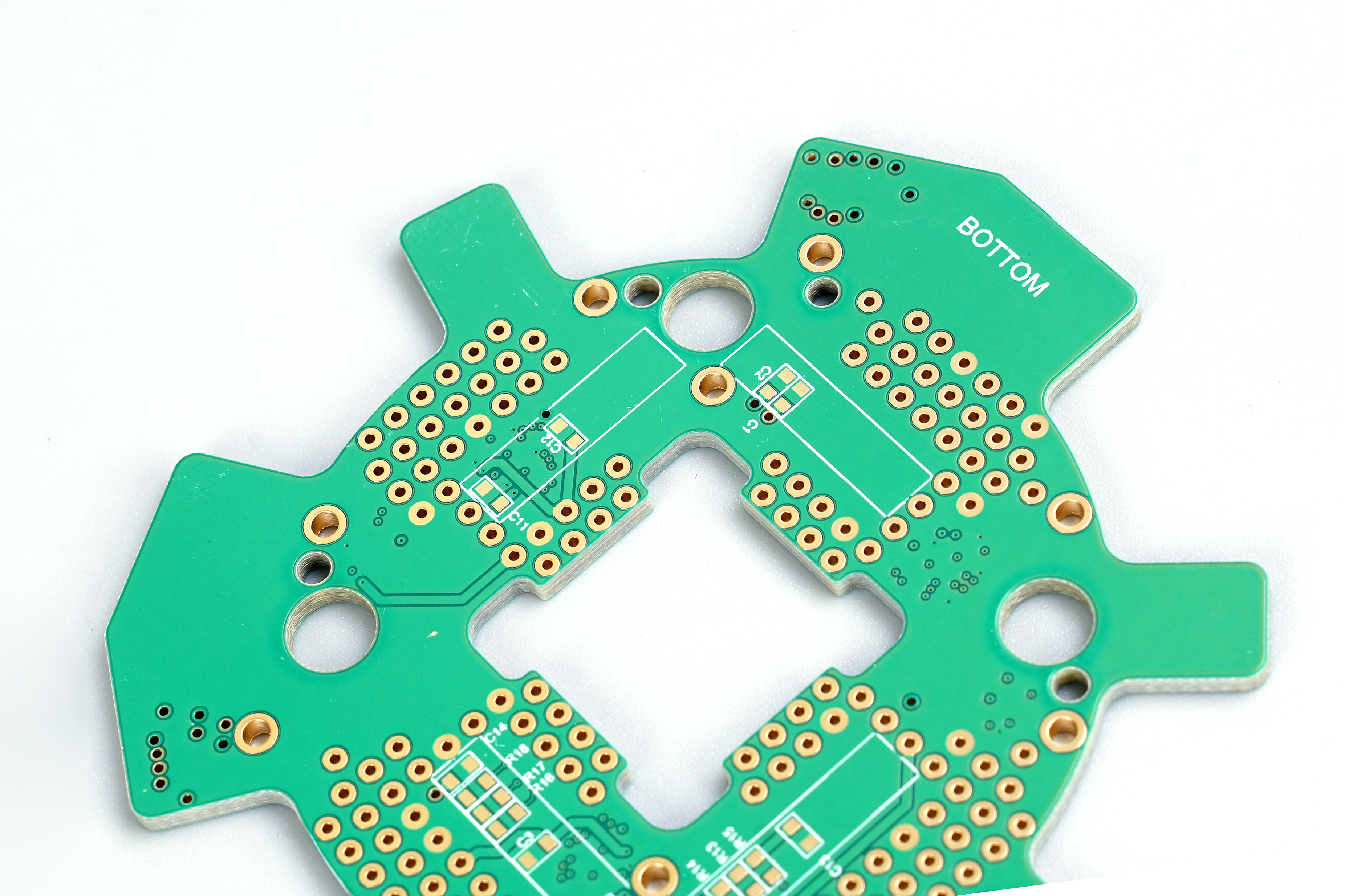
What are circuit boards made of? Are mainly made of a fiberglass epoxy substrate (FR-4) that provides strength and insulation. For special applications, flexible plastic or metal-core materials may also be used.
A thin layer of copper is bonded to the surface and etched into traces to carry electrical signals between components. On top, a solder mask (often green) protects the copper from damage and short circuits, while a silkscreen layer adds labels for assembly and testing.
What Are Printed Circuit Boards Made Of?
Printed circuit boards are made of multiple bonded layers rather than a single material. These layers work together to support electrical connections, protect conductors, and keep the board stable during manufacturing and operation.
At the core of most boards is an insulating substrate. This substrate provides the mechanical foundation of the PCB and prevents unwanted electrical conduction between copper layers. Copper foil is laminated onto this substrate to form traces, pads, and planes that carry signals and power.
Between and around these layers are resin systems that bind everything together. On the outer surfaces, protective coatings such as solder mask are applied to shield copper from oxidation and contamination. Surface finishes are then added to ensure reliable soldering during assembly.
The exact materials vary by application, but the principle remains the same. A PCB is a controlled stack of insulating, conductive, and protective materials designed to work as a single structure.
What Material Are Circuit Boards Made Of?
Circuit boards are made from a combination of insulating materials and conductive metals. No single material can meet all electrical, thermal, and mechanical requirements on its own, so PCBs rely on carefully matched material systems.
The most important insulating materials include fiberglass-reinforced epoxy, polyimide films, ceramic substrates, and metal-backed laminates. These materials prevent electrical shorts while supporting the physical structure of the board.
Copper is the primary conductive material used in circuit boards. It forms the signal traces, power planes, and ground planes that connect electronic components. Copper thickness can vary depending on current requirements and thermal needs.
Resins are used to bond layers together and control properties such as heat resistance and moisture absorption. Protective coatings, including solder mask, protect exposed copper and improve assembly reliability.
What Is the Most Common PCB Material?
The most common PCB material used worldwide is FR4. It is the default choice for a wide range of electronic products, from consumer devices to industrial equipment and many medical systems.
FR4 is widely adopted because it offers a reliable balance between performance and cost. It provides good electrical insulation, strong mechanical stability, and sufficient heat resistance for standard lead-free soldering processes.
Another reason FR4 is so common is consistency. Supply chains for FR4 laminates are mature, making it easy to source in large volumes.
PCB Substrate FR4 Explained
FR4 is a fiberglass-reinforced epoxy laminate. The structure consists of woven glass fiber cloth impregnated with epoxy resin and cured under heat and pressure. This creates a rigid, electrically insulating material with good dimensional stability.
The fiberglass provides strength and resistance to warping. The epoxy resin binds the fibers together and provides insulation. Together, they form a substrate that can withstand mechanical stress and repeated thermal cycles.
FR4 has stable electrical properties for low to moderate frequency applications. Its dielectric constant remains relatively consistent across typical operating temperatures, which supports predictable signal behavior.
There are different grades of FR4. High-Tg FR4 offers improved heat resistance for demanding assemblies. Low-loss FR4 reduces signal attenuation in higher-speed designs. Halogen-free FR4 meets environmental compliance requirements.
Despite these variations, the core concept of PCB substrate FR4 remains the same. It is designed to be reliable, manufacturable, and cost-effective across a wide range of applications.
What Are the Different Types of Circuit Boards?
Circuit boards can be classified by their structure and substrate material. Each PCB type reflects a different material strategy.
Rigid circuit boards are the most common type and are typically made with FR4 substrates. They provide strength and stability for fixed installations.
Flexible circuit boards use thin, bendable substrates such as polyimide. These boards can flex and fold, making them ideal for compact devices and moving assemblies.
Rigid-flex boards combine rigid FR4 sections with flexible interconnects. This design reduces the need for connectors and improves reliability in vibration-sensitive environments.
Metal core circuit boards replace traditional fiberglass substrates with aluminum or copper bases. These boards improve heat dissipation and are widely used in LED lighting and power electronics.
Ceramic circuit boards use materials such as alumina or aluminum nitride. They handle high temperatures and harsh environments, making them suitable for aerospace and industrial applications.
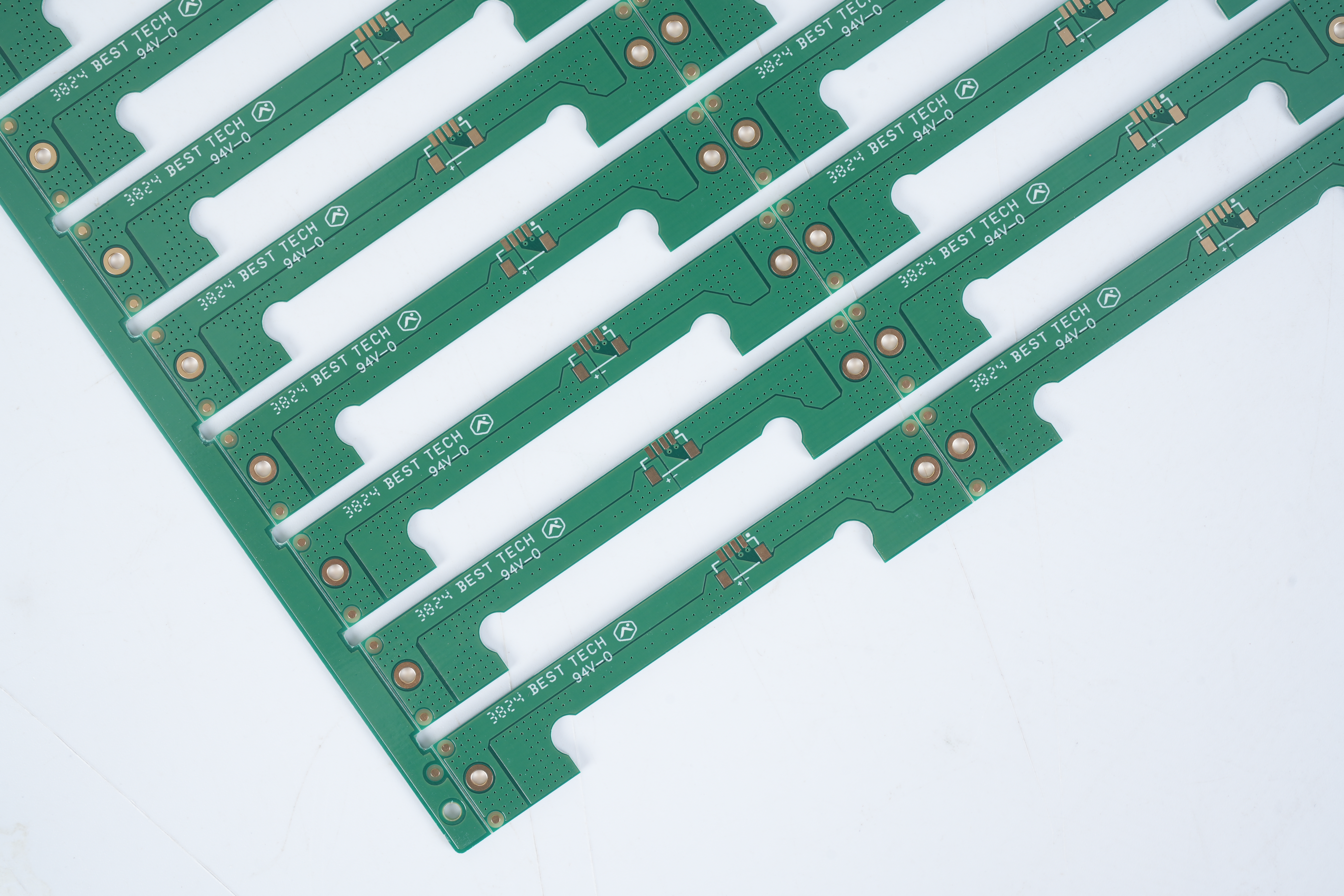
Why Are Circuit Boards Green?
Most circuit boards are green because of the solder mask applied during fabrication. The green color is not chosen for appearance alone. It provides practical benefits during manufacturing and inspection.
Green solder mask offers high contrast against copper traces and silkscreen markings. This makes visual inspection easier for operators and improves accuracy for automated optical inspection systems.
Green solder mask also has stable curing characteristics and consistent performance under heat. It has been refined over decades, making it reliable and widely available.
Although other colors are used for branding or special purposes, green remains the industry standard.
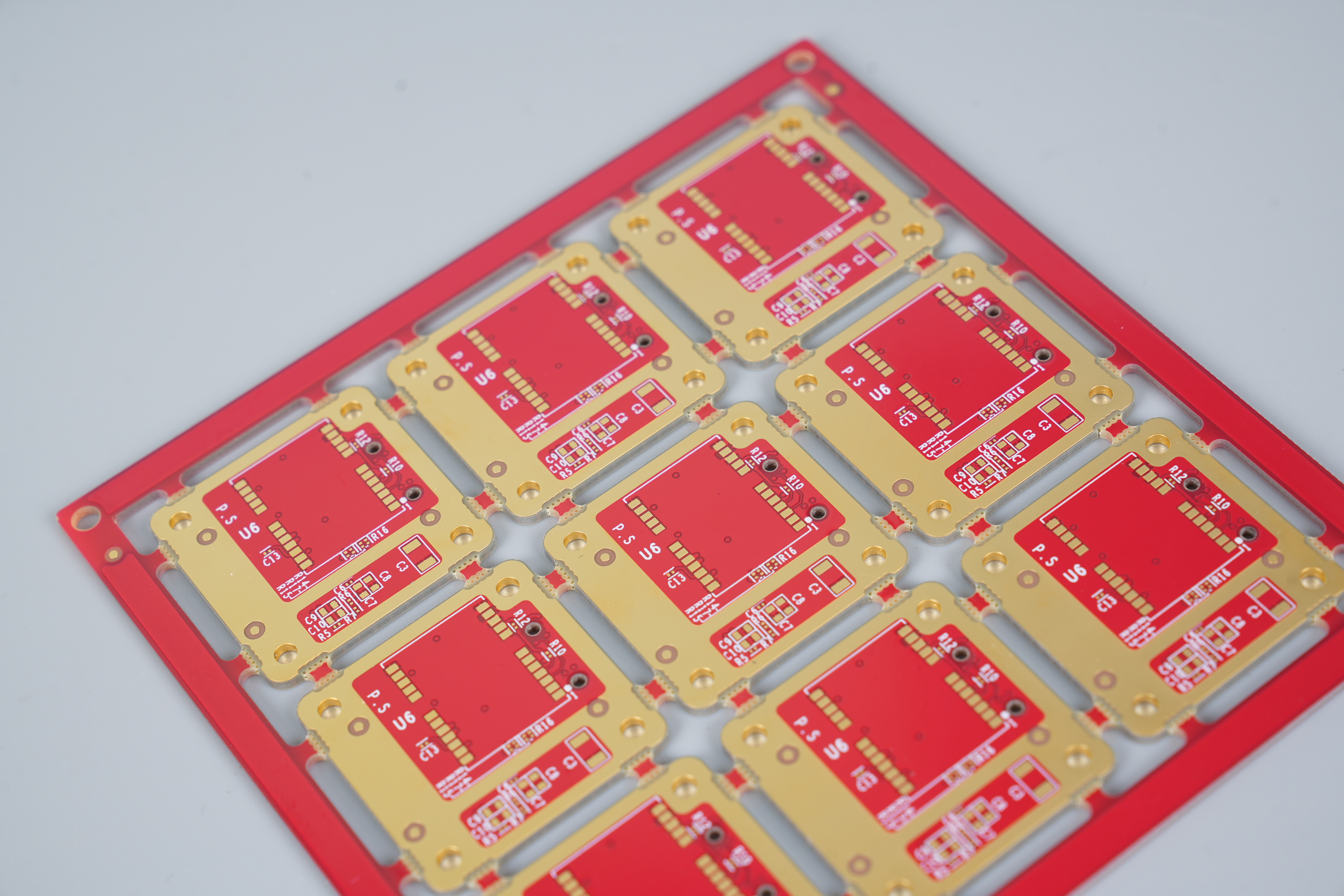
What Are Green Circuit Boards Made Of?
Green circuit boards are made of the same materials as other printed circuit boards. The green color comes solely from the solder mask layer applied to the outer surfaces.
Beneath the green solder mask, the board typically consists of an FR4 or similar insulating substrate, copper conductors, and resin systems that bond the layers together. The solder mask covers copper areas that should not be soldered and leaves openings where components are attached.
The green pigment does not change electrical or thermal performance. Its function is protective and visual rather than structural.
So when asking what are green circuit boards made of, the correct explanation is that they are standard PCBs with a green protective coating on top.
What Is the Purpose of the Solder Mask on a Circuit Board?
The solder mask serves several critical functions on a printed circuit board. Its primary purpose is to prevent solder from flowing onto unwanted areas during assembly.
By insulating exposed copper traces, the solder mask reduces the risk of solder bridges, especially in dense layouts with fine-pitch components. This directly improves assembly yield and reduces rework.
The solder mask also protects copper from oxidation, moisture, and chemical exposure. This protection extends the life of the PCB and improves long-term reliability.
In addition, solder mask openings define where solder paste should be applied. This helps control solder joint shape and consistency, which is important for mechanical strength and electrical performance.
Without solder mask, circuit boards would be far more vulnerable to defects and environmental damage. Its role is essential in modern PCB manufacturing.
Conclusion:
So, what are circuit boards made of? They are built from layered materials that include insulating substrates, copper conductors, resin systems, and protective coatings. Green circuit boards owe their color to solder mask, a layer that protects copper and improves assembly quality.
If you need support selecting PCB substrate material or evaluating PCB substrate types for your project, professional guidance can make a meaningful difference.
For technical inquiries or manufacturing support, please contact: sales@bestpcbs.com
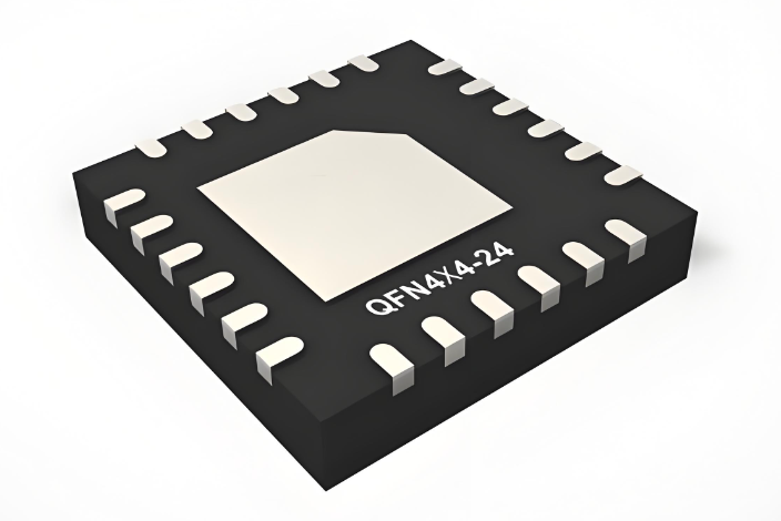
A QFN package, short for Quad Flat No-Lead, is a surface-mount integrated circuit package designed for compact layouts and efficient electrical performance. The term QFN meaning refers to a square or rectangular IC package that uses exposed copper pads instead of protruding leads for electrical connection.
Because of its low profile and short signal paths, QFN has become a preferred choice in modern electronics where space efficiency and signal integrity are critical.
What Does QFN Stand For?
A QFN package (Quad Flat No-Lead) is a surface-mount IC package with exposed pads on the underside instead of protruding leads. Electrical connections are made through metallized terminations located on the package bottom perimeter, often combined with a central exposed thermal pad.
From a manufacturing perspective, QFN packages reduce parasitic inductance and resistance while enabling compact PCB layouts. This is why they are widely used in RF devices, power management ICs, microcontrollers, and high-speed digital components.
Key structural characteristics include:
Flat, leadless body profile
Bottom-side copper pads for electrical connection
Optional exposed pad for thermal and ground connection
Compatibility with standard SMT reflow processes
Types of QFN Packages
QFN packages are available in several structural variations to address different thermal, mechanical, and manufacturing requirements.
Common types include:
Standard QFN – Flat, no-lead design with perimeter pads and optional exposed thermal pad
Wettable Flank QFN – Modified sidewalls that allow visible solder fillets for AOI inspection
Dual-Row QFN – Two rows of pads to support higher pin counts
Air-Cavity QFN – Used in RF and microwave designs to reduce dielectric loss
Each QFN package type balances solderability, inspection capability, and electrical performance differently, which directly impacts PCB assembly strategy.
Advantages of QFN Packages
The popularity of the QFN package is driven by several clear technical advantages.
Key benefits include:
Smaller footprint compared to QFP and other leaded packages
Excellent thermal performance via exposed center pad
Low electrical parasitics, improving signal integrity
Improved mechanical stability due to large solder contact area
Reduced EMI, particularly in high-frequency designs
For dense layouts and performance-critical circuits, QFN often delivers measurable gains over traditional packages.
Disadvantages of QFN Packages
Despite its strengths, the QFN package also introduces specific manufacturing challenges that must be addressed during design and assembly.
Limitations include:
Difficult visual inspection since joints are hidden underneath
Higher assembly sensitivity to stencil design and reflow profile
Rework complexity, especially for center thermal pads
Less forgiving to PCB flatness issues
These drawbacks do not make QFN inferior, but they do demand tighter process control compared to leaded alternatives.
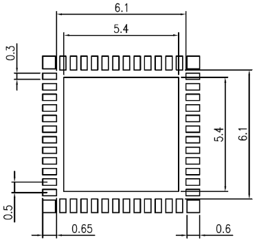
QFN Package Sizes
QFN package sizes are standardized by body dimensions, pin count, and pad pitch, allowing designers to balance I/O density, thermal performance, and routing complexity. While QFN packages are often described simply as “small” or “compact,” the available size range is far broader than many engineers expect.
Common Standard QFN Body Sizes
The following QFN package sizes are widely used across consumer, industrial, and automotive electronics:
2 × 2 mm – Ultra-compact sensors, low-power analog ICs
3 × 3 mm – LDOs, small MCUs, interface ICs
4 × 4 mm – Mixed-signal ICs, power management devices
5 × 5 mm – MCUs, RF transceivers, motor drivers
6 × 6 mm – Connectivity chips, signal processors
7 × 7 mm – High-pin-count controllers, automotive ICs
8 × 8 mm – Power ICs with enhanced thermal needs
10 × 10 mm – High-density logic, networking ICs
12 × 12 mm and larger – RF front ends, industrial control ICs
These sizes are typically specified as body size × body size, not including solder fillets.
QFN Package Sizes by Pin Count
Pin count scales with package size and pad pitch. Typical configurations include:
8–16 pins – 2 × 2 mm to 3 × 3 mm
20–32 pins – 4 × 4 mm to 5 × 5 mm
40–64 pins – 6 × 6 mm to 7 × 7 mm
64–100+ pins – 8 × 8 mm to 10 × 10 mm and above
Higher pin counts often use dual-row QFN designs to maintain reasonable pad pitch while increasing I/O density.
Typical QFN Pad Pitch Options
Pad pitch directly affects PCB routing and soldering tolerance:
0.4 mm – Ultra-fine pitch, HDI recommended
0.5 mm – Common for compact QFN packages
0.65 mm – Easier routing and assembly
0.8 mm – Larger QFN formats with higher power handling
Pad pitch usually ranges from 0.4 mm to 0.65 mm, which directly affects stencil thickness, solder paste selection, and placement accuracy.
How to Solder a QFN Package on PCB?
Soldering a QFN package requires controlled SMT processes rather than manual techniques.
A standard workflow includes:
1. Solder paste printing using a precisely designed stencil
2. Accurate pick-and-place alignment with vision correction
3. Reflow soldering using a controlled temperature profile
4. Post-reflow inspection, typically X-ray rather than AOI
Hand soldering is generally impractical for QFN due to the hidden pads and thermal mass of the exposed center pad.
Key Considerations in QFN Package Soldering
Pad design should match QFN pitches, with the exposed pad extended 0–0.15 mm and 40–60% via opening to balance solder volume and heat dissipation.
Moisture control requires pre-baking QFN components (e.g., 125 °C for 4 hours) to avoid popcorn defects during reflow.
Stencil thickness and aperture design should be optimized (≤0.12 mm, segmented thermal pad openings) to improve paste release and reduce voiding.
Reflow profiling must tightly control ramp rate, soak time, and peak temperature to achieve complete solder activation without component floating.
Manual soldering, if necessary, should use flux-assisted hot-air heating with uniform thermal distribution to avoid localized damage.
Inspection methods should combine edge wetting checks with X-ray analysis to identify hidden solder defects under the package.
How Are QFN Packages Made?
The manufacturing process of a QFN package differs from leaded packages such as QFP.
Typical steps include:
Leadframe stamping or etching
Die attach to exposed thermal pad
Wire bonding to perimeter pads
Mold encapsulation
Singulation into individual packages
Because the package relies on a leadframe rather than formed leads, the result is a compact, mechanically robust IC with excellent thermal conduction paths.
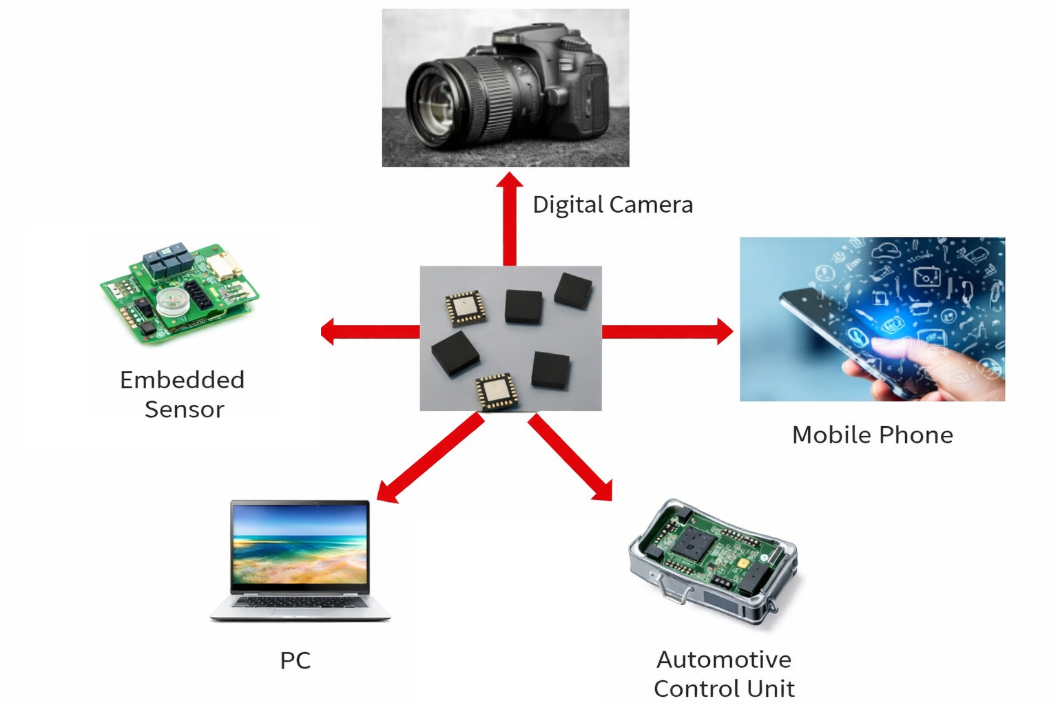
QFN Package Applications
QFN packages are widely adopted across industries that demand compact form factors and stable electrical behavior.
Typical applications include:
Consumer electronics and wearables
RF and wireless communication modules
Automotive control units
Power management ICs
Industrial sensors and embedded controllers
In many of these applications, QFN replaces QFP specifically to reduce board area and improve performance margins.
What Is a QFP Package and How Does It Differ Structurally?
A QFP (Quad Flat Package) uses gull-wing leads extending outward from all four sides of the package body. These visible leads make inspection easier but introduce longer electrical paths and larger footprints.
While QFP packages were once dominant in microcontrollers and ASICs, their size and lead geometry limit their usefulness in modern compact designs.
Structurally, a QFP package features:
External leads visible around the perimeter
Larger pad spacing on the PCB
Easier manual soldering and optical inspection
Increased susceptibility to lead damage during handling
What Is the Difference Between QFN and QFP?
The QFN vs QFP comparison is one of the most common questions during IC selection.
Key differences include:
Aspect
QFN
QFP
Leads
No external leads
Gull-wing leads
Footprint
Smaller
Larger
Thermal performance
Excellent
Moderate
Inspection
X-ray required
Visual AOI possible
Assembly tolerance
Tighter
More forgiving
QFP remains attractive for prototypes and low-complexity designs, while QFN is favored in production-level, space-constrained electronics.
How to Choose the Right IC for Your PCB?
Selecting between a QFN package and a QFP package depends on practical design priorities rather than preference alone.
Consider QFN if:
PCB space is limited
Thermal dissipation is critical
High-speed or RF signals are involved
Consider QFP if:
Easy inspection and rework are required
Assembly capability is limited
The design is still in early prototyping
Matching the package type to your manufacturing maturity is often more important than theoretical performance advantages.
FAQ
1. What does QFN mean in electronics?
QFN means Quad Flat No-Lead, referring to an IC package with bottom-side pads and no protruding leads.
2. Is QFN better than QFP?
QFN is not universally better, but it offers superior size efficiency and thermal performance compared to QFP.
3. Can QFN be hand-soldered?
In most cases, no. QFN requires reflow soldering for reliable results.
4. Why does QFN need X-ray inspection?
Because solder joints are hidden beneath the package, visual inspection is not possible.
5. What surface finish works best for QFN?
ENIG and OSP are commonly used due to their flatness and solderability.
Liechtenstein’s electronic manufacturing sector, focused on industrial control and medical devices, depends on trusted PCB manufacturer in Liechtenstein for high-precision support. Its emphasis on precision drives demand for specialized services, yet balancing speed, cost and EU compliance poses a core challenge. A reliable PCB manufacturer in Liechtenstein must meet strict local standards and tight timelines, making it vital to identify trusted Liechtenstein PCB manufacturers, their capabilities, and pain points.
Top PCB Manufacturer in Liechtenstein
Company Name
Core Business
Key Advantages
Process Capabilities
Lead Time
EBest Circuit Co., Limited
Single/double/multi-layer PCBs for industrial/medical
Localized service, strict QC, EU compliance
HDI, impedance control, ENIG/HASL
7-10d (std), 3-5 day
Triesen Quick-Proto PCB GmbH
Prototypes/low-volume for R&D/startups
R&D-friendly pricing, fast iteration
2-12 layer, laser drilling
1-3d (proto), 4-7day
Liechtenstein Auto-Elec Circuits GmbH
Automotive-grade PCBs for control modules
IATF16949, high-temp resistance
Impedance matching, lead-free finish
9-13d (std), 5-8 day
Balzers IoT PCB Technologie GmbH
IoT sensor PCBs for smart devices
Cost-effective, IoT-focused design
4-8 layer, SMT integration
5-9d (std), 2-4 day
Gamprin Precision PCB GmbH
Multi-layer PCBs for high-end industrial/medical
16-layer capability, strict QA
HDI, blind/buried vias
10-15d (std), 14-20 day
Pain Points of PCB Manufacturer in Liechtenstein
Prototyping delays often occur due to limited local production capacity,failing to meet rapid iteration needs of projects.
High material costs and small order volumes lead to uncompetitive pricing for Liechtenstein PCB prototyping services.
Design inconsistencies with manufacturing capabilities result in rework, as local suppliers lack proactive analysis support.
Strict EU environmental regulations increase production costs, which are often passed on to customers by Liechtenstein PCB factory.
Limited technical support for high-frequency and HDI PCBs, restricting the development of high-end electronic products.
Unstable lead times for bulk orders due to reliance on imported raw materials and components.
Inadequate quality inspection for small-batch orders, leading to potential performance risks in final products.
Full-Process Guarantee from Requirement to Delivery
Pre-production Design Optimization: Provide free DFM analysis to resolve design-manufacturing inconsistencies, reducing rework rates and saving project time for PCB Liechtenstein projects.
Flexible Production Scheduling: Dedicated production lines for prototyping and small batches, eliminating delays caused by capacity constraints and ensuring rapid response.
Cost Control System: Bulk material procurement and optimized production processes to offer competitive pricing without compromising quality for Liechtenstein PCB manufacturing.
Compliance-Oriented Production: Integrate EU environmental standards into every process, ensuring products meet REACH and RoHS requirements without additional costs.
High-End Technical Support: Professional team specialized in high-frequency and HDI PCBs, providing customized solutions for complex Liechtenstein PCB needs.
Stable Supply Chain: Global strategic partnerships with raw material suppliers to avoid lead time fluctuations for bulk orders.
Full-Process Quality Inspection: Implement AOI automatic detection and manual full inspection for all orders, regardless of batch size, to ensure zero defective products delivery.
Real-Time Order Tracking: Digital management system allows customers to monitor production progress anytime, enhancing transparency for PCB manufacturer in Liechtenstein services.
Why Choose EBest(Best Technology) for PCB Manufacturer in Liechtenstein?
Competitive Pricing: Optimize cost structure via bulk material procurement, average reducing Liechtenstein PCB project budgets by 15%-20%, with transparent pricing no hidden costs.
24-Hour Rapid Prototyping: Dedicated emergency lines, finish prototyping in 24 hours for 6-layer and below standard specs, matching urgent iteration needs.
High On-Time Delivery Rate: 99.2% on-time delivery for all orders, supported by global supplier partnerships and intelligent production scheduling.
Strict Quality Control: 18-process full inspection (AOI/X-ray/electrical testing), product yield stable above 99.5%, zero defective delivery guaranteed.
19 Years of Industry Experience: Deep expertise in Liechtenstein PCB manufacturing, serving 500+ local clients, optimizing processes to cut 10% unnecessary costs.
Free DFM Analysis: Proactive pre-production optimization, reducing design rework rate by 40%+, shortening project cycles by 72 hours on average.
Comprehensive Certifications: Hold ISO9001:2015, ISO13485:2016, IATF16949, AS9100D, REACH & RoHS, covering 100% local high-end industry requirements.
Localized Service: Nearby service center with ≤4-hour response, 200+ annual on-site support for Liechtenstein PCB company partners.
Customized Solutions: Support 2-32 layer PCB customization, 60%+ order volume for small batches, adapting to diverse technical demands.
Liechtenstein PCB Prototyping Service We Can Offer
Our rapid prototyping service is tailored for Liechtenstein PCB projects, addressing the core pain points of local quick-turn needs with technical strength and efficient delivery. Equipped with 3 dedicated emergency production lines and mature precision manufacturing capabilities, we balance speed and accuracy to support rapid project iteration. We cover 2-24 layer prototyping, with minimum line width/spacing of 3mil/3mil and warpage controlled at ≤0.3%, ensuring compatibility with complex designs.
Unlike local services plagued by capacity constraints, our one-stop prototyping supports diverse processes (ENIG, HASL, OSP) and materials (FR-4, aluminum substrate), with impedance deviation controlled within ±10% for high-frequency demands. This combination of speed, precision and flexibility cuts local prototyping cycles by 40%+, making us the trusted partner for urgent, high-quality PCB Liechtenstein prototyping needs.
1. Submit Clear Requirements: Send standardized design files (Gerber, DXF) along with specific demands — material type (e.g., FR-4, aluminum substrate), layer count, surface finishing (ENIG/HASL/OSP), and order quantity. Files can be submitted via email or our official platform, with a recommended naming format for quick sorting.
2. Free Professional Evaluation: For standard Liechtenstein PCB prototyping requests, our team completes DFM analysis (to pre-check manufacturability and optimize designs) and cost assessment within 2 hours, reducing potential rework risks upfront.
3. Transparent Quotation Confirmation: Receive a detailed quotation with itemized costs, clear lead time commitment, and corresponding quality standards. No hidden fees — all expenses (processing, material, testing) are fully disclosed.
4. Simplified Order Placement: Confirm the quotation and pay the deposit (30% of total amount as standard). We immediately issue an order confirmation with detailed production milestones, including pre-production check and delivery cutoff times.
5. Real-Time Progress Tracking: Monitor Liechtenstein PCB manufacturing progress via our digital system anytime. Automatic notifications are sent for key nodes (production start, quality inspection, shipment), ensuring full process transparency.
Welcome to contact us if you have any request for PCB prototyping: sales@bestpcbs.com.
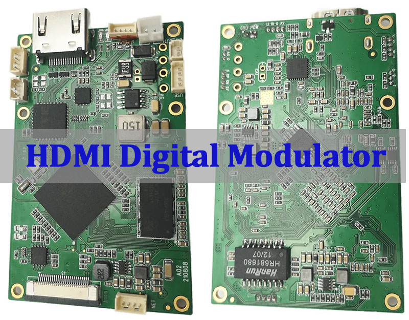
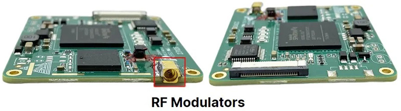
An HDMI digital modulator is a critical device that converts high-definition multimedia interface (HDMI) signals into broadcast-standard RF signals for distribution over coaxial cable networks. This article delves into the core PCB design and PCBA manufacturing challenges and services required to build reliable digital HDMI modulators.
Developing a high-performance HDMI modulator often exposes design teams to a set of tightly coupled PCB and PCBA challenges.
Extremely Complex PCB Layout High-speed HDMI, digital processing, and RF circuitry must coexist on dense multi-layer boards.
Severe Signal Interference Crosstalk, EMI, and noisy power rails degrade RF modulation quality.
Thermal Management Issues Heat from FPGAs, encoders, and RF stages impacts stability and lifetime.
Component Sourcing & Assembly Risks Fine-pitch BGAs, RF shielding, and long-lifecycle IC availability increase build difficulty.
Inconsistent Yield and Performance PCB impedance variation and SMT process drift reduce production yield.
Addressing these risks requires a PCB and PCBA partner with proven experience in high-speed and RF-integrated designs.
Advanced Multi-Layer PCB Design 8+ layer stack-ups with controlled impedance and clear digital/RF partitioning.
Signal and Power Integrity Control Pre-layout and post-layout analysis to suppress EMI and crosstalk.
Thermal and Reliability Engineering Optimized materials, thermal vias, and heat dissipation strategies.
DFM-Driven Component Procurement Verified sourcing combined with assembly-focused design optimization.
Targeted Functional and RF Testing ICT, RF signal validation, and thermal stress testing for each HDMI digital RF modulator.
At EBest Circuit (Best Technology), we are a specialized PCB fabrication and turnkey PCBA assembly manufacturer focused on complex, high-frequency, and mixed-signal PCB and PCBA products like modulators. Our core advantage lies in comprehensive DFM analysis and BOM optimization, supported by R&D, PCB, and PCBA engineers with over 20 years of hands-on experience, who provide practical manufacturing-focused recommendations to ensure your HDMI digital modulator PCB or SMT design is optimized for reliable mass production. Contact us at sales@bestpcbs.com to transform your design into a robust product.
What Is an HDMI Digital Modulator From a PCB and PCBA Perspective?
From a PCB and PCBA standpoint, an HDMI digital modulator is a convergence of several high-performance electronic subsystems on a single, complex printed circuit board. Its core function—encoding and modulating an HDMI stream into an RF signal—dictates a challenging integration of diverse technologies.
High-Speed Digital Interface: The HDMI input stage requires a multi-gigabit serial link, demanding controlled impedance routing (typically 100Ω differential) and strict length matching on the PCB.
Digital Processing Core: An FPGA or dedicated encoder chip performs video compression (e.g., MPEG-2/H.264) and multiplexing. This area requires dense BGA fanouts, clean power planes, and often external DDR memory.
RF Modulation & Upconversion: This is the heart of the digital HDMI to RF modulator. A DAC and mixer translate the digital stream to an intermediate frequency (IF), which is then upconverted to the target RF channel (e.g., QAM, ATSC, DVB-T). PCB layout here is critical to avoid noise injection.
Power Management Network: Multiple, isolated voltage rails (e.g., 1.0V, 1.8V, 3.3V, 5V) with low noise are needed for different ICs. This involves switch-mode regulators and LDOs, placed to minimize switching noise interference.
Output Conditioning & Protection: The final RF signal passes through amplifiers, SAW filters, and protection circuits before reaching the F-connector. Transmission line integrity up to the connector is paramount.
In essence, the PCB for an HDMI digital encoder modulator is a carefully orchestrated platform where digital signal integrity, RF purity, and thermal management must coexist. The PCBA process must then accurately populate and solder this sophisticated board.
How a Digital HDMI Modulator Is Implemented on a Multi-Layer PCB?
Implementing a digital HDMI modulator requires a carefully planned multi-layer PCB architecture to manage high-speed signal routing, power integrity, RF isolation, and thermal performance. In practice, an 8–12 layer stack-up is commonly used to separate functional domains and ensure stable operation.
Typical Multi-Layer PCB Stack-Up Overview
Layer
Primary Function
Key Considerations
L1 (Top)
Components, HDMI & RF signals
Controlled-impedance routing
L2
Solid ground plane
Clean return path, shielding
L3
Digital signal routing
Control and logic signals
L4
Power plane (Core voltage 1)
Noise-sensitive digital power
L5
Power plane (RF / analog)
Isolated RF power regions
L6
Internal digital signals
FPGA / encoder switching
L7
Solid ground plane
Reference for bottom signals
L8 (Bottom)
Power & large components
Regulators, bulk passives
The stack-up structure prioritizes signal reference integrity, power isolation, and RF containment rather than routing density alone.
Functional Partitioning of the PCB
Partitioning is critical in HDMI digital modulator designs. The PCB is divided into clearly defined zones:
HDMI input and TMDS processing
Digital processing (FPGA / encoder)
RF synthesis and modulation
RF output and matching network
Physical separation between these zones minimizes coupling between noisy digital sections and sensitive RF circuitry.
RF Shielding and Grounding Strategy
Sensitive RF blocks such as VCOs, mixers, and output drivers are protected using:
Grounded copper pour fences on the top layer
Dense via stitching tying fences to internal ground planes
Short, low-inductance ground connections
This approach effectively creates localized Faraday cages that suppress EMI and prevent digital noise from contaminating the RF spectrum.
Via Structure and Thermal Management
A combination of via types is required to support both signal escape and thermal control:
Through vias for general connectivity
Blind and buried vias for dense BGA fan-out
Thermal vias under FPGAs, encoders, and RF amplifiers
Thermal vias conduct heat into internal planes or toward bottom-side heatsinks, improving long-term reliability and frequency stability.
It is clear that this structured, multi-layer PCB methodology is essential for building a stable and manufacturable HDMI digital RF coaxial modulator. It allows HDMI processing, digital control, and RF modulation subsystems to operate concurrently without mutual interference, while maintaining consistent performance across production volumes.
Key PCB Design Challenges in an HDMI Digital RF Modulator
Designing the PCB for an HDMI digital RF modulator presents a unique set of challenges where digital and RF design disciplines collide. Success hinges on anticipating and mitigating these issues from the first layout.
Mixed-Signal Coexistence & Isolation: The primary challenge is isolating the noisy digital domain (FPGA, switching regulators) from the sensitive RF analog domain. This requires careful floor planning, the use of separate ground planes that are tied together at a single point (often near the power input), and strategic placement of moats (splits in power planes).
Impedance Control Across the Board: Different signals have different requirements:
HDMI: 100Ω differential pairs.
RF Traces: 50Ω single-ended (e.g., from mixer to amplifier).
DDR Memory: Specific single-ended impedance (e.g., 40Ω). The PCB stack-up must be calculated to achieve these impedances simultaneously across different layers and trace widths.
Thermal Management at the PCB Level: High-power components (FPGA, RF PA) concentrate heat. The PCB itself must act as a heat spreader. This involves using thick copper planes (2oz+), arrays of thermal vias under components, and designing keep-out areas under thermally sensitive parts like crystal oscillators.
Power Integrity (PI) Design: The digital core can draw current in large, fast bursts, causing voltage droop. A robust PI network involves using multiple decoupling capacitors of different values (bulk, ceramic) placed very close to IC power pins, and ensuring low-impedance power delivery networks (PDNs) through wide planes and short connections.
Material Selection for RF Performance: While FR-4 is sufficient for digital sections, the final RF output stage, especially for higher frequencies or in an HDMI digital QAM modulator, may require a low-loss, stable dielectric material like Rogers (RO4350B) for the critical RF traces to minimize signal attenuation and phase noise.
Addressing these challenges requires not just software skill, but profound experience in mixed-signal and RF PCB design—a core service for a reliable manufacturing partner.
Why HDMI Digital COAX Modulator Designs Require Careful Signal Integrity Control?
The “COAX” in HDMI digital COAX modulator underscores its final output: a clean, broadcast-quality RF signal on a coaxial cable. Signal Integrity (SI) control is the discipline that ensures the digital bits are accurately transformed into this analog waveform, free from distortion that could disrupt video reception.
Clock Integrity is Paramount: Any jitter (timing noise) in the system clock or the video pixel clock can propagate through the encoding and modulation chain, manifesting as phase noise in the RF output. This leads to a degraded modulation error ratio (MER) and pixelation on screens. Careful, isolated routing of clock lines with guard traces is essential.
Managing Return Paths: High-speed signals follow the path of least inductance back to their source. If a discontinuity (like a split in the reference ground plane) exists under a critical trace, the return current will find an alternative, longer path, creating a loop antenna and radiating EMI. Ensuring uninterrupted ground planes beneath all high-speed traces is a fundamental SI rule.
Controlling Crosstalk: Aggressive routing in dense areas can cause crosstalk, where energy from one trace couples to another. In a modulator, crosstalk from a digital bus into an RF or clock trace can introduce spurious noise. SI practices like maintaining 3W spacing (trace center-to-center spacing equal to three times the trace width) between sensitive lines mitigate this.
Transmission Line Effects at RF: At the operating frequency of the RF output (e.g., 50-1000 MHz), even short traces behave as transmission lines. Impedance mismatches at connectors or component pads cause reflections, leading to standing waves and reduced output power. Perfect 50Ω matching from the modulator IC output to the F-connector is the goal.
In summary, SI control in a digital COAX to HDMI modulator (or its more common counterpart, the HDMI to coax device) is what separates a functional prototype from a reliable, high-performance product suitable for commercial deployment.
HDMI Digital QAM Modulator Architecture and Its Impact on PCBA Assembly
An HDMI digital QAM modulator employs Quadrature Amplitude Modulation to deliver high data rates over cable systems. Its architecture directly influences the complexity and requirements of the PCBA assembly process.
The core chain involves: HDMI Input -> Encoder (MPEG/H.264) -> QAM Modulator IC (with DAC) -> RF Upconverter -> SAW Filter & Power Amplifier -> Output.
This architecture impacts PCBA assembly in several key ways:
Fine-Pitch Components: The QAM modulator and encoder chips often come in fine-pitch QFN or BGA packages (pitch ≤ 0.4mm). This demands:
High-precision solder paste stencil printing.
Advanced SMT placement machines with high accuracy and vision systems.
A controlled reflow soldering profile to ensure proper solder joint formation without bridging or voids.
Sensitive RF Passives: The upconverter stage uses tiny 0201 or 01005-sized inductors and capacitors for matching networks. Their precise placement and soldering are critical for RF performance; even minor misalignment can shift the center frequency or impact output power.
Shielding Can Requirements: To prevent external interference and contain EMI, critical RF sections are often covered with metal shielding cans. This adds a secondary soldering operation (can attachment) and complicates post-assembly inspection and rework. Designs must include a proper PCB landing pattern for the shield.
Test Point Access: The architecture necessitates numerous test points for verifying digital data streams, intermediate frequencies (IF), and final RF power/MER. The PCBA layout must provide physical access for probe tips, which can be challenging in dense layouts, especially under shields.
Therefore, assembling an HDMI digital RF QAM modulator is not a standard SMT job. It requires a PCBA partner with the equipment, process controls, and experience to handle high-density, mixed-technology assembly while maintaining RF integrity.
PCBA Process Considerations for an HDMI Digital ATSC Modulator
An HDMI digital ATSC modulator, designed for the North American Advanced Television Systems Committee standard, has specific PCBA process needs to ensure it meets strict broadcast regulations.
RF Performance-Centric Stencil Design: The solder paste stencil aperture design must be optimized not just for preventing bridging on fine-pitch ICs, but also for depositing the correct volume of paste under RF component pads (like those for SAW filters) to ensure reliable electrical connection and minimal insertion loss.
Controlled Atmosphere Reflow: Using Nitrogen (N2) inert atmosphere during reflow soldering is highly recommended. It reduces oxidation, improves solder wetting for better joint quality, and is crucial for achieving reliable solder joints with lead-free SAC alloys, which are standard for professional equipment.
Conformal Coating for Reliability: Modulators may be deployed in uncontrolled environments (e.g., headends, hotel distribution closets). Applying a conformal coating protects the PCBA from humidity, dust, and minor condensation, enhancing long-term reliability. Masking of connectors and test points is a critical step.
Programmable Device Configuration: The FPGA or system-on-chip will require firmware/bitstream loading. The PCBA process flow must include a step for in-circuit programming (ICP) after assembly, often using a bed-of-nails fixture or a dedicated programming header.
Special Handling for Crystals & VCOs: The temperature-compensated crystal oscillator (TCXO) or voltage-controlled oscillator (VCO) that sets the RF carrier frequency is extremely sensitive to mechanical stress and thermal shock. Process guidelines must minimize board flex and ensure a gentle thermal profile during soldering.
Adherence to these specialized processes is what ensures a digital HDMI ATSC modulator board is not just assembled, but built for stable, long-term operation in the field.
Single Channel Digital HDMI Modulator vs Multi Channel HDMI Digital Modulator in Manufacturing
Choosing between a single channel digital HDMI modulator and a multi channel HDMI digital modulator directly impacts PCB complexity, PCBA scalability, thermal design, and overall manufacturing cost.
Manufacturing-Oriented Comparison Overview
Aspect
Single-Channel Modulator
Multi-Channel Modulator
PCB Design
Compact, lower complexity
Large, high-density, complex
Component Count
Low
High, channel-dependent
Thermal Profile
Localized heat
Distributed high heat
Power Architecture
Simple, low current
Multi-rail, high current
Testing Effort
Short, straightforward
Long, parallel testing
Primary Cost Driver
Components
PCB, assembly, testing
Manufacturing Implications Behind the Comparison
From a production standpoint, single channel digital HDMI modulator builds focus on process repeatability and yield optimization for a relatively simple PCB. The primary challenges lie in fine-tuning impedance control, HDMI signal integrity, and first-pass SMT yield.
In contrast, multi channel HDMI digital modulator manufacturing shifts the challenge toward managing system-level complexity. Replicated HDMI encoding and modulation blocks dramatically increase routing density, thermal load, and power distribution requirements. Yield becomes more sensitive to PCB variation, assembly tolerances, and cumulative thermal effects across channels.
Testing strategy also diverges significantly. Single-channel units can rely on sequential functional validation, while multi-channel designs demand parallel RF and video testing to keep test time and cost under control.
To put it simply, successfully producing both architectures requires a PCBA partner capable of scaling from precision-driven low-complexity builds to high-density, multi-channel system boards, without sacrificing consistency or throughput. Experience with parallel testing, thermal mitigation, and yield control becomes critical as channel counts increase.
SMT Assembly and Testing Challenges in a Multi Channel HDMI Digital RF Modulator
The SMT assembly and testing of a multi channel HDMI digital RF modulator represent the peak of manufacturing complexity for this product category, integrating all previous challenges at a larger scale.
Yield Management on High-Value PCBs: The board incorporates numerous high-cost components (FPGAs, multiple RF ICs). A single soldering defect can render the entire expensive assembly scrap. Processes like Automated Optical Inspection (AOI) and X-Ray inspection for BGAs are mandatory after reflow to catch defects early.
Consistent RF Performance Across Channels: Achieving identical output power, MER, and frequency accuracy for all 4 or 8 channels is difficult. Variations can stem from:
Solder paste volume differences on matching networks.
Slight misalignment of RF components.
Minor inconsistencies in PCB laminate properties across the board panel. Tight process control and statistical process monitoring are essential.
Thermal Warpage During Reflow: Large, dense PCBs are prone to warping during the high-temperature reflow cycle. This can cause open connections (head-in-pillow defects) on large BGA components. Using high-Tg PCB materials and a customized, multi-zone reflow profile with appropriate support in the oven is critical.
Comprehensive Functional Testing Complexity: Testing a single-channel unit involves one HDMI input and one RF output. Testing an 8 channel HDMI digital modulator requires simultaneously feeding 8 HDMI sources and analyzing 8 RF outputs—a significant increase in test fixture complexity, automation, and time. Developing a streamlined, multi-port test system is a major project in itself.
Overcoming these challenges requires a manufacturer with not just assembly capability, but true engineering partnership—offering DFM feedback to simplify assembly, investing in advanced process and test equipment, and possessing the expertise to troubleshoot subtle, channel-to-channel performance variations.
As a final remark, HDMI digital modulators are sophisticated bridges between modern digital video and legacy RF distribution systems, and their reliability is fundamentally determined by their PCB design and PCBA quality. This article has explored the critical considerations, from multi-layer PCB implementation and signal integrity to the nuanced assembly requirements of different modulator types like QAM, ATSC, and multi-channel variants.
At EBest Circuit (Best Technology), we specialize in transforming complex designs—such as HDMI digital RF modulator PCBs and multi channel HDMI digital RF modulator PCBAs—into reliable, high-yield products. Our expertise in advanced PCB fabrication, precision SMT assembly, and rigorous testing is tailored to meet the exacting standards of broadcast and professional AV electronics. Pls feel free to contact our team anytime at sales@bestpcbs.com to discuss your project.
What Is Performance Qualification (PQ) in Medical PCBA Production?
Performance Qualification (PQ) is the documented verification that a validated medical PCBA manufacturing process consistently produces assemblies that meet defined quality and regulatory requirements under normal production conditions.
After Installation Qualification (IQ) confirms that equipment is correctly installed, and Operational Qualification (OQ) confirms that assembly processes operate reliably within defined limits, PQ answers the final and most practical question: Can this process repeatedly deliver compliant medical PCBAs in real production?
For medical electronics, PQ represents the transition from engineering validation to dependable manufacturing reality.
Why Is PQ Essential for Medical PCBA Manufacturing?
Medical devices often operate continuously, support diagnostic decisions, or perform life-sustaining functions. In these applications, a process that works once is not enough.
PQ is essential because it:
Demonstrates long-term process stability
Confirms consistency across operators, shifts, and lots
Reduces the risk of latent defects entering the field
Provides objective evidence for regulatory inspections
Builds OEM confidence for volume production
From a regulatory standpoint, PQ is often the final gate before full production approval.
How Does PQ Differ From Engineering Trials or Pilot Builds?
Engineering trials and pilot builds are typically conducted under controlled conditions with close supervision. PQ, by contrast, is intentionally performed under routine manufacturing conditions.
This means PQ uses:
Standard production operators
Normal shift schedules
Approved work instructions
Regular inspection and test methods
The objective is not to demonstrate ideal performance, but to confirm repeatable, sustainable output under everyday conditions.
How Is Performance Qualification (PQ) Conducted for Medical PCBA?
In medical PCBA production, PQ usually involves multiple production runs designed to represent normal manufacturing variability.
At Best Technology, a typical PQ approach includes:
Manufacturing multiple lots using standard processes
Running production across normal shifts
Applying routine AOI, X-ray, and functional testing
Collecting yield, defect, and rework data
Reviewing trends rather than single-lot results
This approach ensures that performance conclusions are based on process behavior over time, not isolated success.
What Metrics Are Commonly Evaluated During PQ?
PQ focuses on indicators that reflect real manufacturing performance and product reliability. Common metrics include:
First-pass yield (FPY)
Defect rate and defect trends
Rework frequency and causes
Functional test pass rates
Stability of critical process outputs
These metrics help demonstrate that the process remains in control and predictable, which is critical for regulated medical products.
Why Is PQ Especially Important for Medical Device Reliability?
Medical PCBAs may be exposed to long operating hours, thermal cycling, or repeated use over extended lifetimes. Even small variations in assembly quality can accumulate into failures.
PQ provides assurance that:
Quality does not degrade across batches
Process drift is identified and controlled
Assemblies meet specification consistently over time
For diagnostic, monitoring, and life-support devices, PQ is often examined closely during regulatory audits because it directly reflects real-world manufacturing reliability.
What Risks Exist If PQ Is Weak or Incomplete?
Inadequate PQ can lead to serious downstream consequences, including:
Production instability after scale-up
Increased field failure rates
Corrective and preventive actions (CAPA)
Product recalls or shipment holds
Loss of OEM trust
In medical electronics, these risks affect not only manufacturing efficiency but also patient safety and regulatory standing.
IQ vs OQ vs PQ: How Do They Compare in Medical PCBA Validation?
The table below summarizes the distinct roles of IQ, OQ, and PQ within medical PCBA process validation:
Qualification Stage
Primary Focus
Key Question Answered
Typical Scope
When It Is Performed
IQ (Installation Qualification)
Equipment & environment
Is everything installed correctly?
Machines, systems, utilities, calibration
Before process testing
OQ (Operational Qualification)
Process capability
Does the process work within defined limits?
Printing, placement, reflow, cleaning, testing
After IQ
PQ (Performance Qualification)
Production consistency
Can we produce compliant boards consistently?
Yield, defects, trends, real production output
After OQ
Together, these stages form a closed-loop validation framework required for medical PCBA manufacturing.
How Does PQ Build on IQ and OQ?
PQ only has regulatory value when it is supported by solid IQ and OQ foundations:
IQ ensures the manufacturing environment is properly installed
OQ ensures the process is capable and controlled
PQ confirms consistent performance under routine production
Without IQ and OQ, PQ results lack context. Without PQ, IQ and OQ remain theoretical.
How Does Best Technology Support PQ for Medical PCBA Projects?
Best Technology supports medical PCBA customers with a structured PQ approach aligned with ISO 13485 expectations, including:
Stable, validated SMT and test processes
Full production traceability
Data-driven yield and defect analysis
Documentation suitable for OEM and regulatory review
This ensures that medical PCBA production is not only compliant, but sustainably reliable at scale.
How Does PQ Fit Into the Complete Medical PCBA Validation Series?
Performance Qualification is the final confirmation that a medical PCBA process is ready for long-term production. To fully understand its role, it is recommended to review the earlier stages of this series:
What Is Operational Qualification (OQ) in Medical PCBA Assembly?
Operational Qualification (OQ) is the documented evidence that each step of the medical PCBA assembly process operates reliably within predefined and approved operating limits. After Installation Qualification (IQ) confirms that equipment and systems are correctly installed, OQ focuses on a more critical question: does the process actually work as intended under controlled variation?
In medical electronics manufacturing, OQ represents the technical core of process validation. It is where engineering intent, manufacturing capability, and regulatory expectations converge.
Why Is OQ a Critical Requirement for Medical PCBA Manufacturing?
Medical devices rely on electronics that must perform consistently over long service lives, often in safety-critical or continuously operating environments. Final inspection alone cannot guarantee this level of reliability.
OQ is critical because it:
Demonstrates that assembly processes are capable, stable, and repeatable
Defines acceptable process windows rather than relying on nominal settings
Reduces dependence on operator judgment
Provides objective evidence for regulatory audits and OEM reviews
From a regulatory perspective, OQ shows that process risks are understood and controlled, not discovered after failures occur.
Which Assembly Processes Are Typically Validated During OQ?
In medical PCBA assembly, OQ usually covers all process steps that can influence product quality, reliability, or compliance. At (EBest Circuit) Best Technology, typical OQ scope includes:
Component placement: accuracy across different package sizes, fine-pitch components, and placement repeatability
Reflow soldering: temperature profiles validated at minimum and maximum limits, including soak, peak, and cooling zones
Cleaning processes: effectiveness in meeting ionic contamination requirements
Conformal coating (if applicable): thickness consistency, coverage, and curing parameters
Functional and in-circuit testing: stability of results across defined operating ranges
Each process is evaluated not only at nominal conditions but also near its upper and lower operating limits.
How Does OQ Define Safe Process Windows?
One of the primary goals of OQ is to establish validated process windows. Instead of asking whether a process works once, OQ asks whether it continues to work when conditions vary within controlled boundaries.
For example:
Can solder joints remain reliable if reflow peak temperature shifts slightly?
Does placement accuracy remain acceptable across different component densities?
Does cleaning effectiveness remain consistent at different throughput levels?
By answering these questions, OQ transforms unknown variability into documented, acceptable ranges, which is essential for medical PCBA reliability.
Why Is OQ Especially Important for Medical Electronics?
Medical PCBAs often involve:
Fine-pitch and micro-pitch components
High-density interconnects
Mixed SMT and through-hole assembly
Sensitive analog, sensing, or signal-conditioning circuits
These characteristics make medical electronics highly sensitive to process variation. Minor deviations can create latent defects such as marginal solder joints or intermittent connections that pass inspection but fail during use.
OQ reduces this risk by ensuring that assembly processes remain stable even when operating near their defined limits.
How Does OQ Reduce Manufacturing and Patient Risk?
By validating process behavior under controlled variation, OQ helps prevent:
Weak or inconsistent solder joints
Thermal overstress or insufficient soldering
Operator-dependent outcomes
Process drift over time
In medical applications, such issues are not merely quality concerns—they can directly impact device safety, regulatory compliance, and patient outcomes. OQ provides the engineering evidence that these risks are actively managed.
What Do Auditors and Medical OEMs Expect From OQ Documentation?
During audits or supplier qualification reviews, OQ documentation is often examined in detail. Auditors and OEMs typically expect to see:
Clearly defined and justified process parameters
Evidence that limits were intentionally challenged
Repeatable and reproducible results
Documented handling of deviations or anomalies
Well-structured OQ records demonstrate that the manufacturer understands its processes at an engineering level, rather than relying on empirical success alone.
How Does OQ Differ From IQ and PQ?
Although IQ, OQ, and PQ are closely related, each serves a distinct purpose:
IQ confirms that equipment and systems are installed correctly
OQ confirms that processes operate reliably within defined limits
PQ confirms consistent output under normal production conditions
OQ acts as the bridge between installation and production, translating equipment capability into process control.
How Does (EBest Circuit) Best Technology Perform OQ for Medical PCBA Projects?
This approach ensures that medical PCBA assembly processes are not only functional, but technically understood and defensible.
What Comes After OQ in Medical PCBA Validation?
While OQ confirms that processes are capable, it does not yet prove long-term consistency in real production environments. That confirmation is provided by Performance Qualification (PQ), which evaluates routine manufacturing stability across multiple lots and operators.
Related reading:
Performance Qualification (PQ) in Medical PCBA Production
To fully understand how OQ fits within the complete validation framework, it is also recommended to review:
Installation Qualification (IQ) is the documented verification that all equipment, systems, and infrastructure used in medical PCBA manufacturing are installed correctly and conform to approved specifications.
In regulated medical electronics, IQ is not a procedural formality; it is the foundation of process validation.
Before evaluating solder quality, yields, or test results, manufacturers must first prove that the manufacturing environment itself is controlled, traceable, and suitable for medical production. IQ provides this proof in a structured and auditable manner.
Why Is IQ the First Step in Medical PCBA Process Validation?
Medical regulations emphasize process control over end-product inspection. A compliant output cannot compensate for an uncontrolled environment.
IQ is performed first because it:
Establishes baseline manufacturing conditions
Confirms equipment configuration and utilities
Locks approved software and hardware versions
Creates traceable records for future audits
Without IQ, subsequent validation activities such as OQ and PQ lack regulatory credibility.
Which Equipment and Systems Are Included in Medical PCBA IQ?
At Best Technology, IQ for medical PCBA projects typically covers:
SMT pick-and-place machines, including placement accuracy and software revision
Solder paste printing systems and stencil alignment capability
Reflow and curing ovens, including zone configuration and atmosphere control
AOI, SPI, and X-ray inspection systems
Electrical and functional test platforms
ESD protection infrastructure
MES-based traceability systems
Calibration tools and measurement equipment
Each item is verified against predefined installation requirements, including environmental conditions, utilities, configuration, and calibration status.
Why Is IQ Required for Medical PCBA Compliance?
Medical regulations such as ISO 13485 emphasize process control over final inspection. IQ provides documented proof that the manufacturing environment is controlled, repeatable, and auditable.
IQ is essential because it:
Prevents undocumented equipment substitution
Establishes a validated baseline for audits
Supports long-term traceability for regulated devices
Reduces regulatory risk during design transfer and scale-up
Without IQ, even functional medical PCBAs may be considered non-compliant during audits.
What Are the Risks of Skipping or Weak IQ in Medical PCBA?
Incomplete or missing IQ documentation can lead to:
Audit nonconformities
Delayed supplier qualification
Re-validation requirements
Increased regulatory exposure for OEMs
Even when PCBAs pass electrical testing, lack of IQ can result in formal non-acceptance during audits or regulatory reviews.
How Does Best Technology Implement IQ for Medical PCBA Projects?
Best Technology applies a structured IQ approach that includes:
Approved equipment lists and installation records
Verification of utilities and environmental conditions
Calibration status confirmation
MES and traceability validation
Controlled documentation aligned with medical audits
This ensures a repeatable and defensible foundation for all downstream validation activities.
What is the Relation Between IQ and OQ?
IQ confirms that the manufacturing environment is correctly installed, but it does not validate process performance. Once installation is confirmed, manufacturers must demonstrate that assembly processes operate reliably within defined limits. This is achieved through Operational Qualification (OQ).