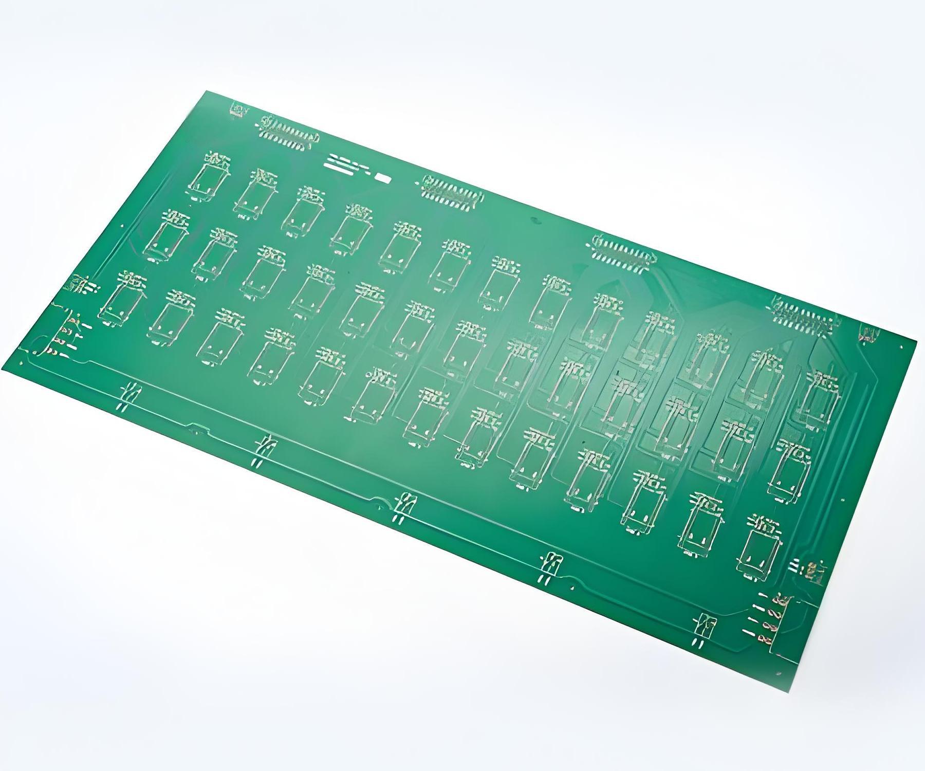
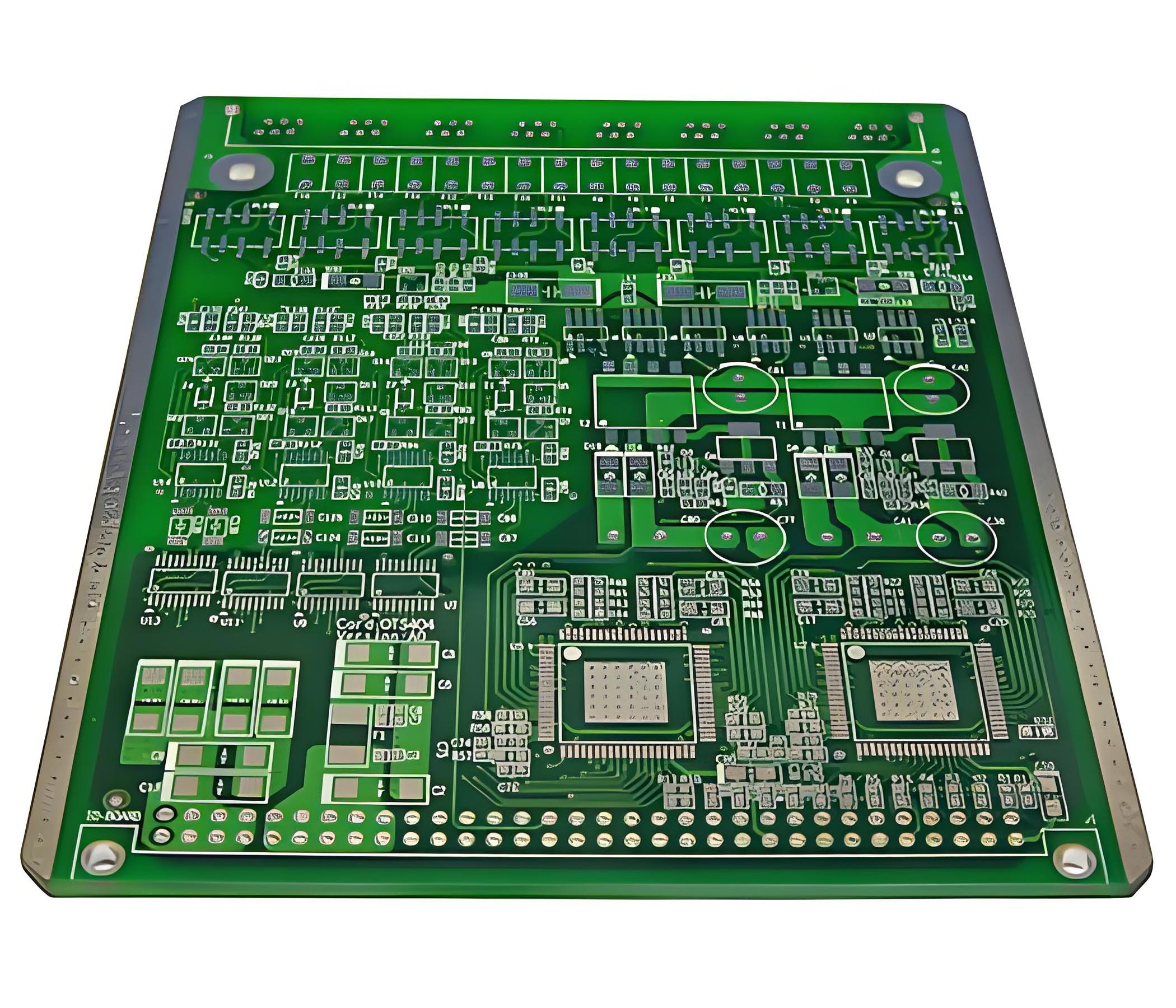
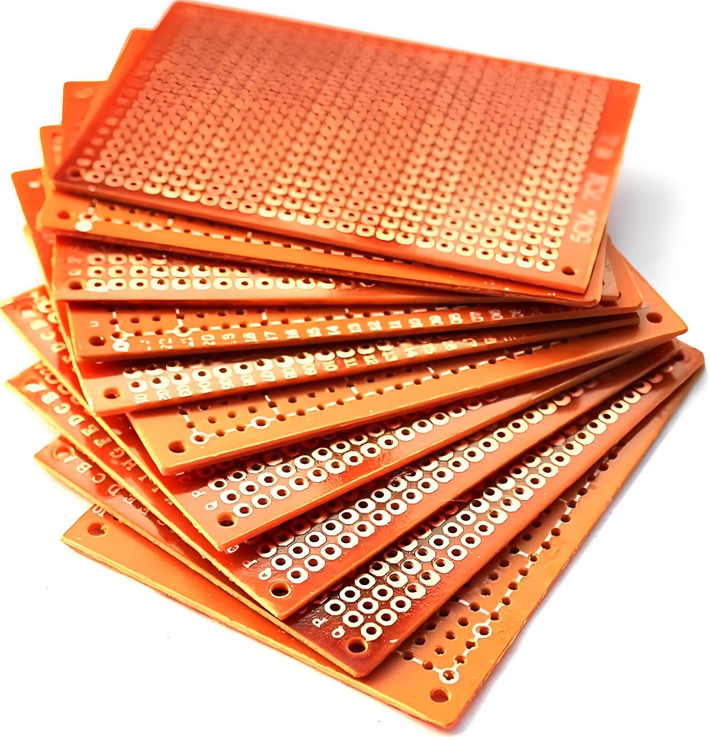
Aluminum base PCB (Printed Circuit Board) is an essential part of modern electronics, particularly for applications where heat dissipation is critical. These PCBs are designed to provide effective heat management, which is why they are widely used in high-power LED systems, automotive electronics, and other devices that generate significant heat. In this article, we’ll explore the key features of aluminum base PCBs, including their thermal properties, construction, and benefits compared to other PCB materials.
What is Aluminum PCB?
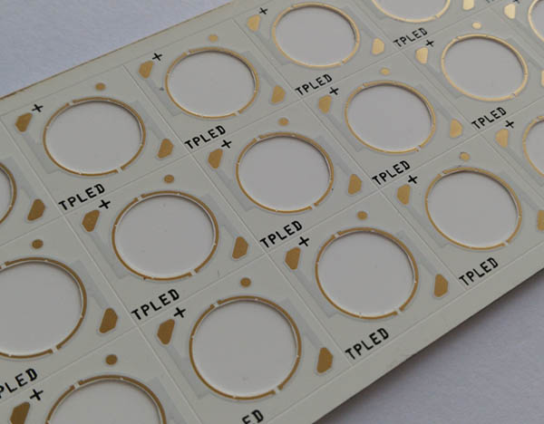
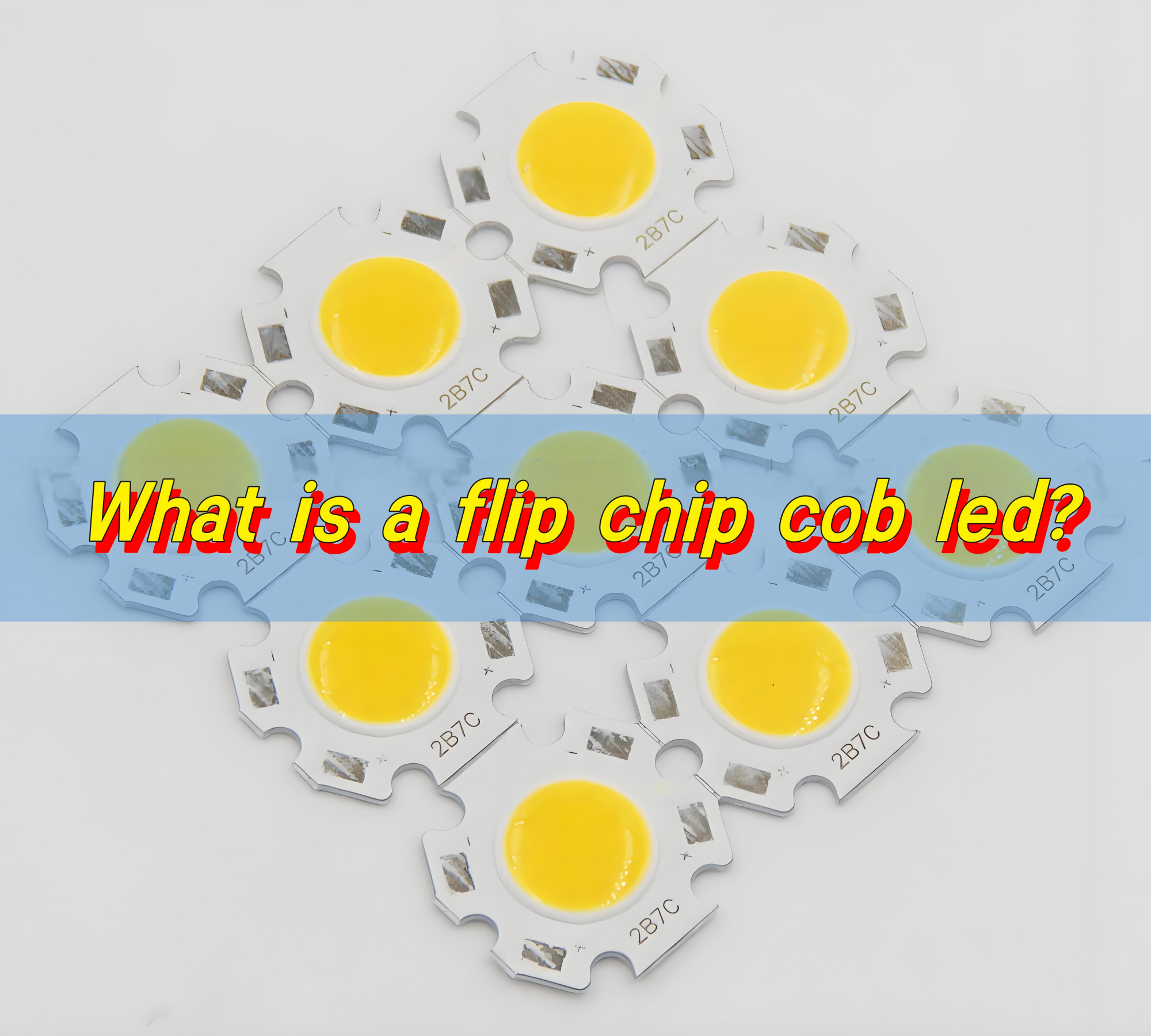
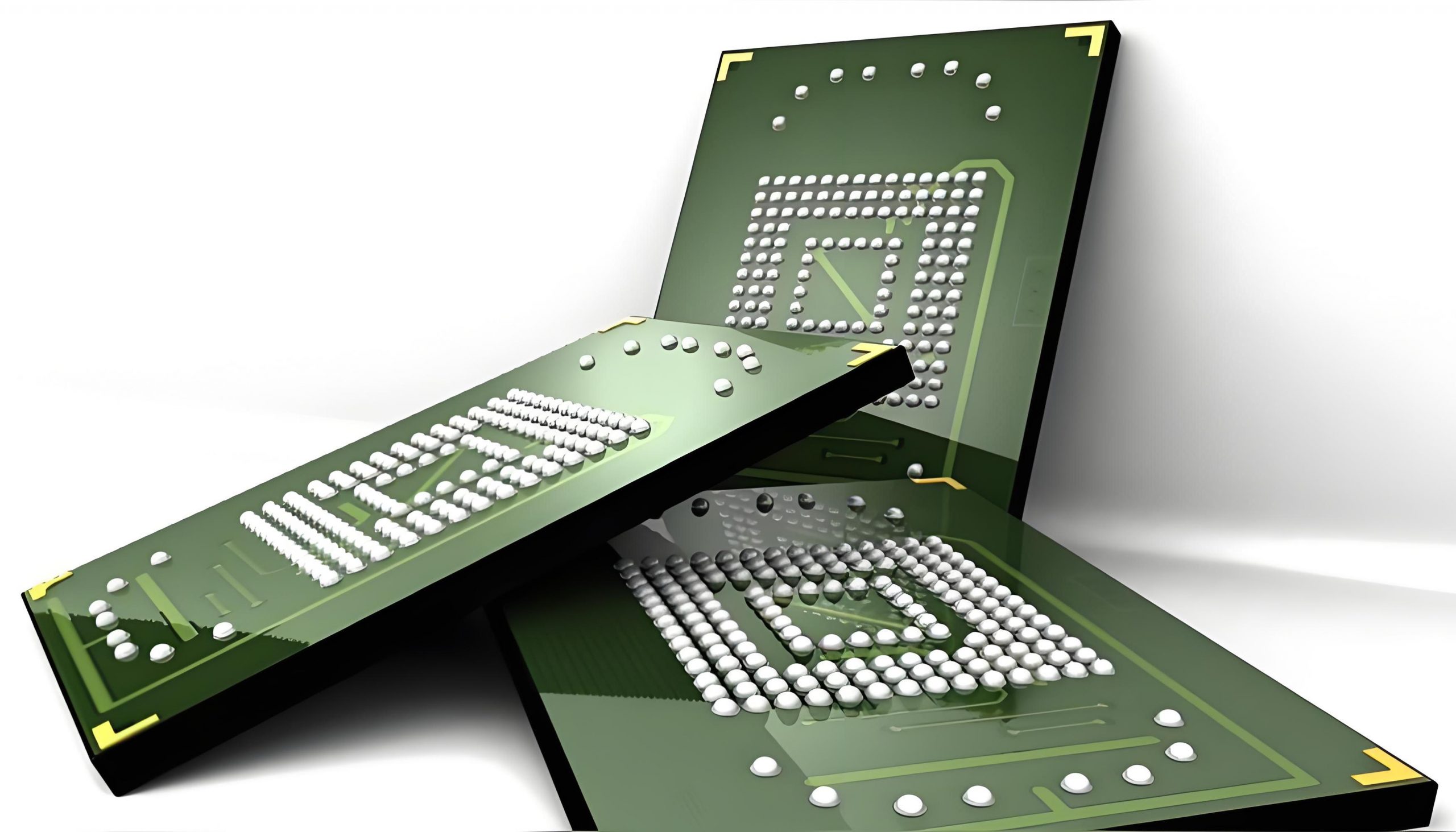
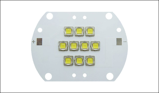
An aluminum PCB is a type of metal-based PCB that uses an aluminum substrate to provide better thermal conductivity. The aluminum material acts as both a conductor for electrical signals and a heat sink to dissipate heat away from sensitive components. Aluminum PCBs are typically used in high-power applications where managing heat is a crucial concern, such as in LED lighting, power supplies, and automotive electronics.
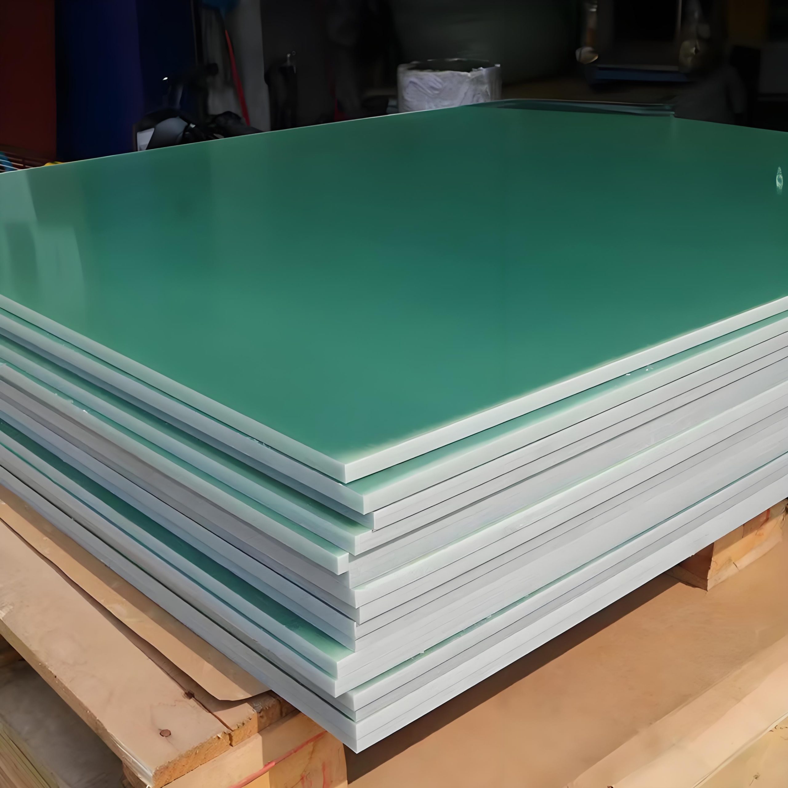
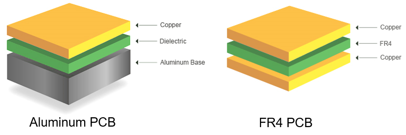
The design of aluminum base PCBs consists of three layers: the copper layer, the dielectric layer, and the aluminum base. The copper layer carries the electrical signals, while the dielectric layer insulates and binds the copper to the aluminum base. This combination ensures both electrical efficiency and heat management.

What is the Thermal Resistance of Aluminum PCB?
The thermal resistance of an aluminum PCB refers to how well the PCB can resist heat transfer. In most cases, aluminum PCBs have a low thermal resistance, meaning they efficiently transfer heat away from the components. The thermal resistance of aluminum substrates is usually between 1.0 and 3.2℃/W. Most aluminum substrates have a thermal resistance greater than 1℃/W, while high thermal conductivity aluminum substrates have a thermal resistance less than 0.5℃/W or lower. For example, the thermal resistance of a tin-sprayed aluminum substrate can reach 1.7℃/W or 3.2℃/W. The specific thermal resistance can depend on the thickness of the copper and dielectric layers, but generally, aluminum PCBs are known for their superior heat dissipation properties.
In comparison to traditional FR4 PCBs, aluminum-based PCBs offer much better thermal management, making them a popular choice for power-hungry devices like high-power LEDs. This efficient heat dissipation helps to maintain the stability and performance of the device, preventing overheating and reducing the risk of failure.
What is the Maximum Temperature for Aluminum PCB?
The maximum temperature an aluminum PCB can withstand depends on the design and the materials used. However, most aluminum base PCBs can operate effectively at temperatures ranging from -40°C to 150°C(Even higher, but may be limited in long-term use). Some specialized designs can even handle more higher temperatures.
Aluminum PCBs are often chosen for their ability to operate in high-temperature environments without compromising performance. This makes them an excellent choice for industries like automotive, telecommunications, and lighting, where high temperatures are common.
How Thick is Aluminum PCB?
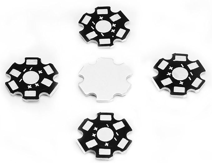
The thickness of an aluminum PCB can vary depending on its application and the heat dissipation requirements. Typically, the aluminum base layer ranges from 0.8mm to 3.0mm, with thicker layers providing better heat dissipation. The thickness of the copper layer also plays a role, as thicker copper helps to better handle high-power applications.
For instance, a 12w LED aluminum base PCB would typically use a copper thickness of about 1 oz/ft² to 2 oz/ft², whereas a 25w LED aluminum base PCB would require a thicker copper layer to handle the increased power. Thicker aluminum layers are used in devices that generate significant heat, such as LED drivers and power supplies.
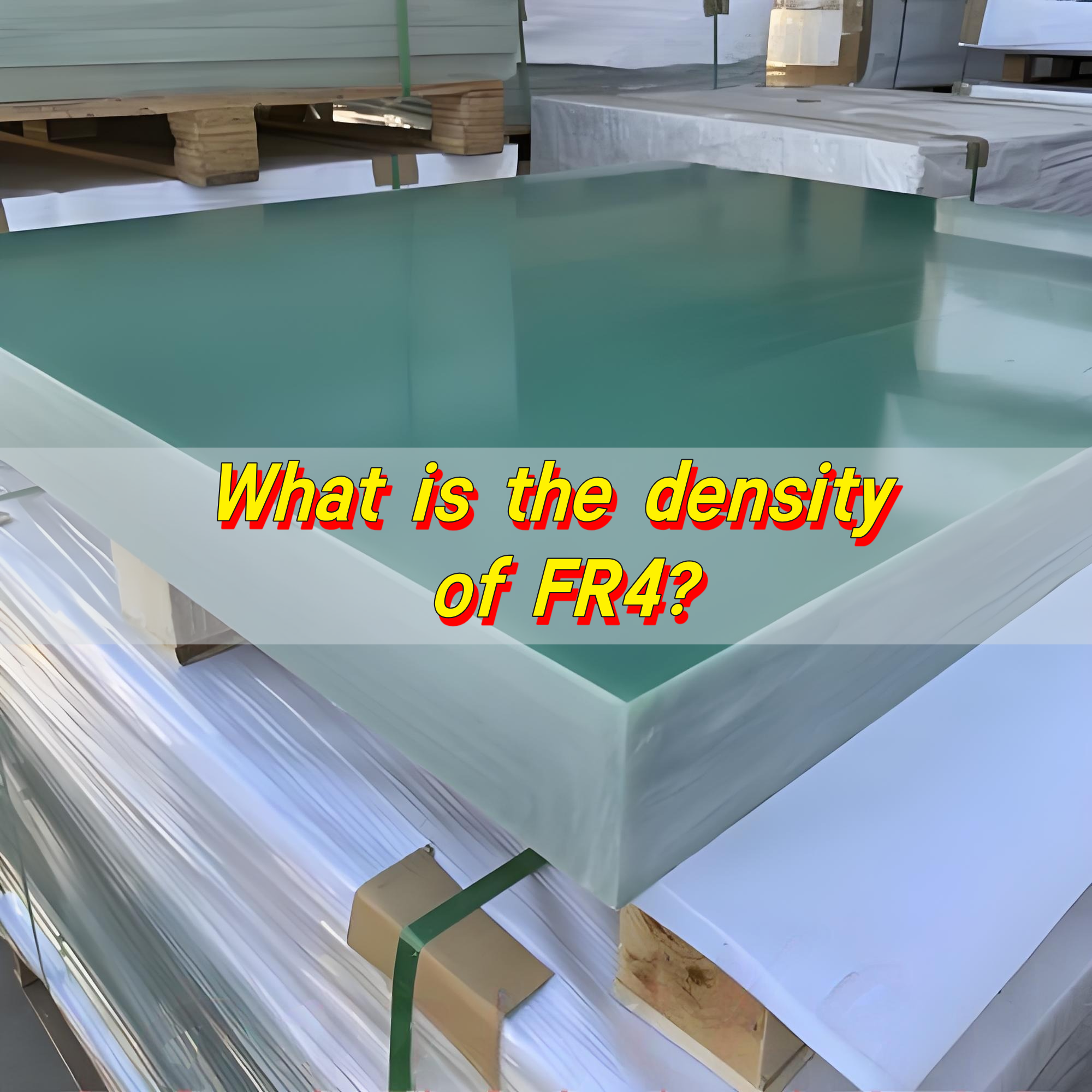
What is the Difference Between FR4 and Aluminum PCB?
The primary difference between FR4 PCBs and aluminum PCBs lies in their substrate material. FR4 is a composite material made of woven fiberglass and epoxy resin, while aluminum PCB uses aluminum as the base layer.
FR4 is widely used for general applications because it is cost-effective and offers good electrical insulation. However, it doesn’t provide the same level of heat dissipation as aluminum PCBs. Aluminum-based PCBs, on the other hand, are specifically designed to manage heat more effectively, which is why they are preferred for high-power applications like aluminum base LED PCBs and metal-based aluminum PCBs.
Another key difference is that aluminum PCBs are generally thicker and more rigid than FR4 boards, offering better mechanical strength. While FR4 is a great choice for lower-power devices, aluminum PCBs are the go-to solution for heat-intensive applications. EBest Circuit (Best Technology) stands out by providing customized, high-quality products with quick turnaround times, all backed by our top-tier customer service.
What is the Best PCB Material for Heat Dissipation?
Aluminum is the best material for heat dissipation when it comes to PCBs. Aluminum base PCBs excel in transferring heat away from sensitive components, ensuring that devices do not overheat during operation. Other materials like copper and ceramic also have good thermal properties, but aluminum provides a balanced combination of cost, performance, and manufacturability.
For high-power devices like LED aluminum base PCBs or metal-based aluminum PCB boards, aluminum is the material of choice due to its excellent thermal conductivity, which helps maintain the optimal performance and longevity of the device.
How Do Aluminum PCBs Work?
Aluminum PCBs work by using the aluminum base to conduct heat away from the components mounted on the board. When an electronic component, such as an LED, operates, it generates heat. In a traditional PCB made from materials like FR4, this heat can build up, causing the components to overheat and potentially fail.
With aluminum PCBs, the heat generated by the components is quickly transferred through the copper and dielectric layers to the aluminum base. From there, the heat is dissipated into the surrounding environment, preventing overheating. This process ensures that the components remain within their safe operating temperature range, thus improving the reliability and lifespan of the device.
For example, aluminum-based LED PCBs are specifically designed to handle the high heat generated by LEDs, keeping them cool and allowing them to operate efficiently without degradation.
Aluminum base PCBs offer superior thermal management, making them ideal for high-power applications that require efficient heat dissipation. From aluminum base LED PCBs to metal-based aluminum PCB boards, these PCBs help prevent overheating, increase reliability, and improve the overall performance of electronic devices. Whether you are designing a 25w PCB LED aluminum star base or a single layer LED aluminum base PCB, aluminum offers excellent heat resistance and thermal conductivity.
When selecting the right PCB material, aluminum base PCBs should be at the top of your list for any application where heat management is a priority. With their ability to handle high temperatures and provide better mechanical strength than traditional materials like FR4, aluminum-based PCBs are the best choice for applications such as LED lighting, power supplies, and other high-power electronics.
Choose aluminum base PCBs for your next project and experience improved performance, longer lifespan, and efficient heat management. EBest Circuit (Best Technology) offers a wide range of aluminum base pcb products with high quality, tailored to meet the specific needs of each customer. Pls feel free to reach out to us at sales@bestpcbs.com for more details.