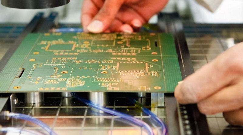
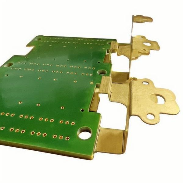
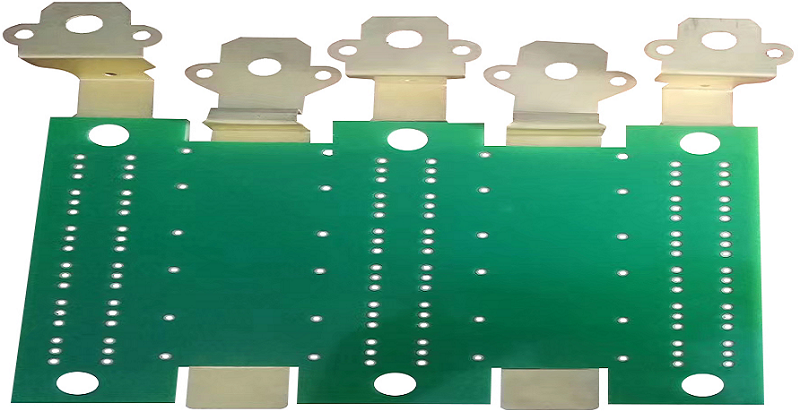
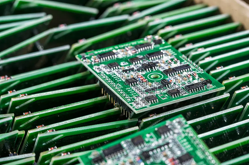
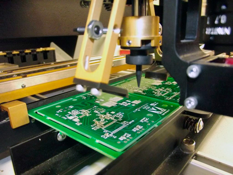
Solid state drive SSD PCB design requires reasonable layout of controllers, flash memory chips, power management modules and interfaces (such as SATA or NVMe), optimization of power supply and ground plane to reduce noise, and consideration of heat dissipation solutions to ensure efficient data transmission and stable operation.

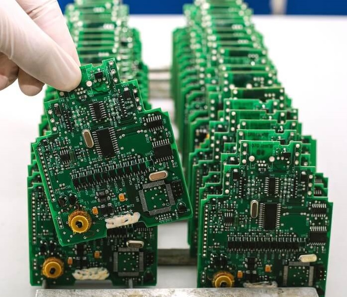
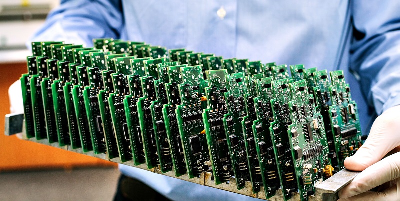
At EBest Circuit (Best Technology), we specialize in high-quality SSD PCB design and manufacturing, offering expert solutions for both consumer and enterprise-grade SSDs. With cutting-edge technology, advanced thermal management, and top-grade materials, we ensure your SSD PCBs deliver optimal performance and reliability.
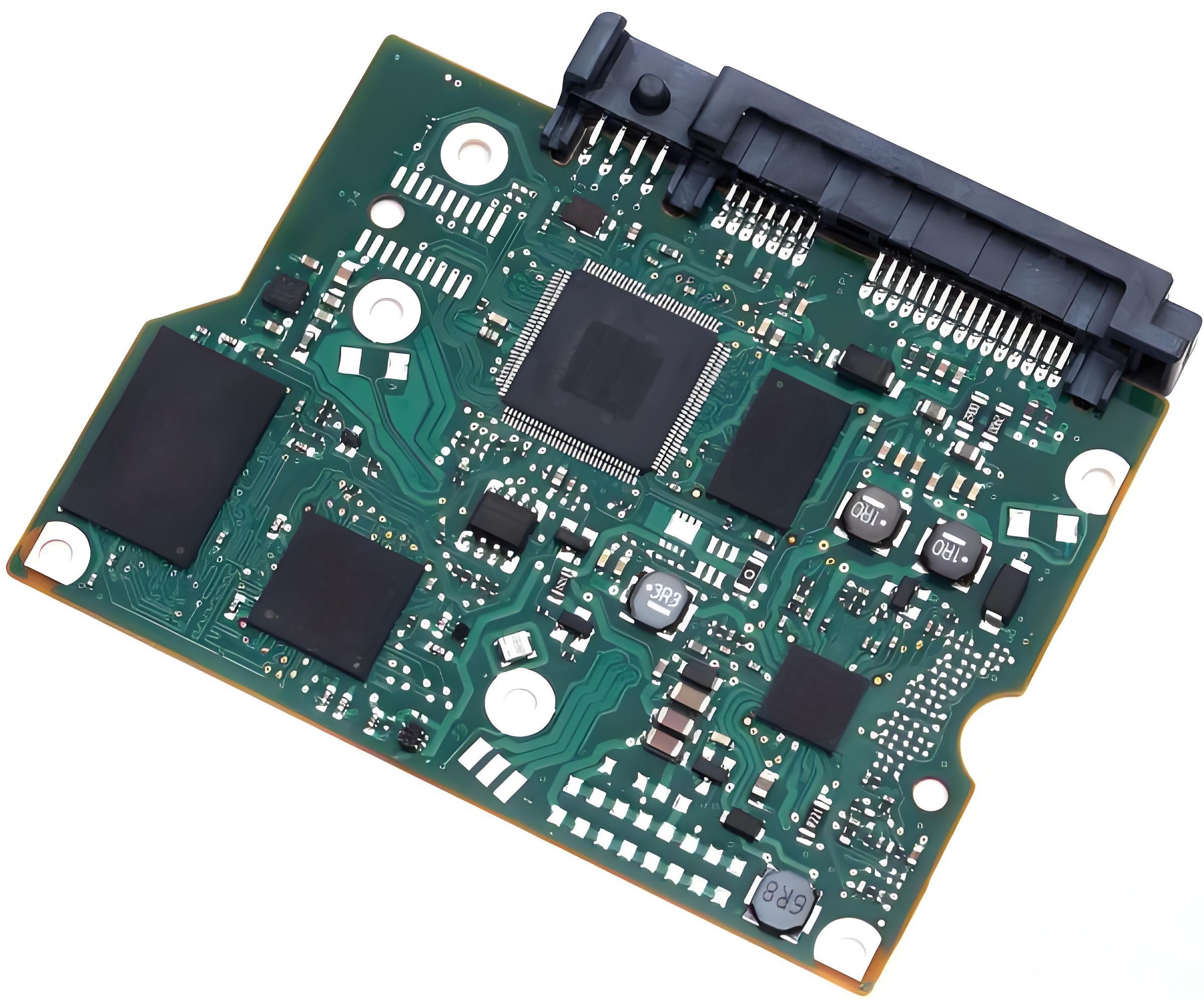
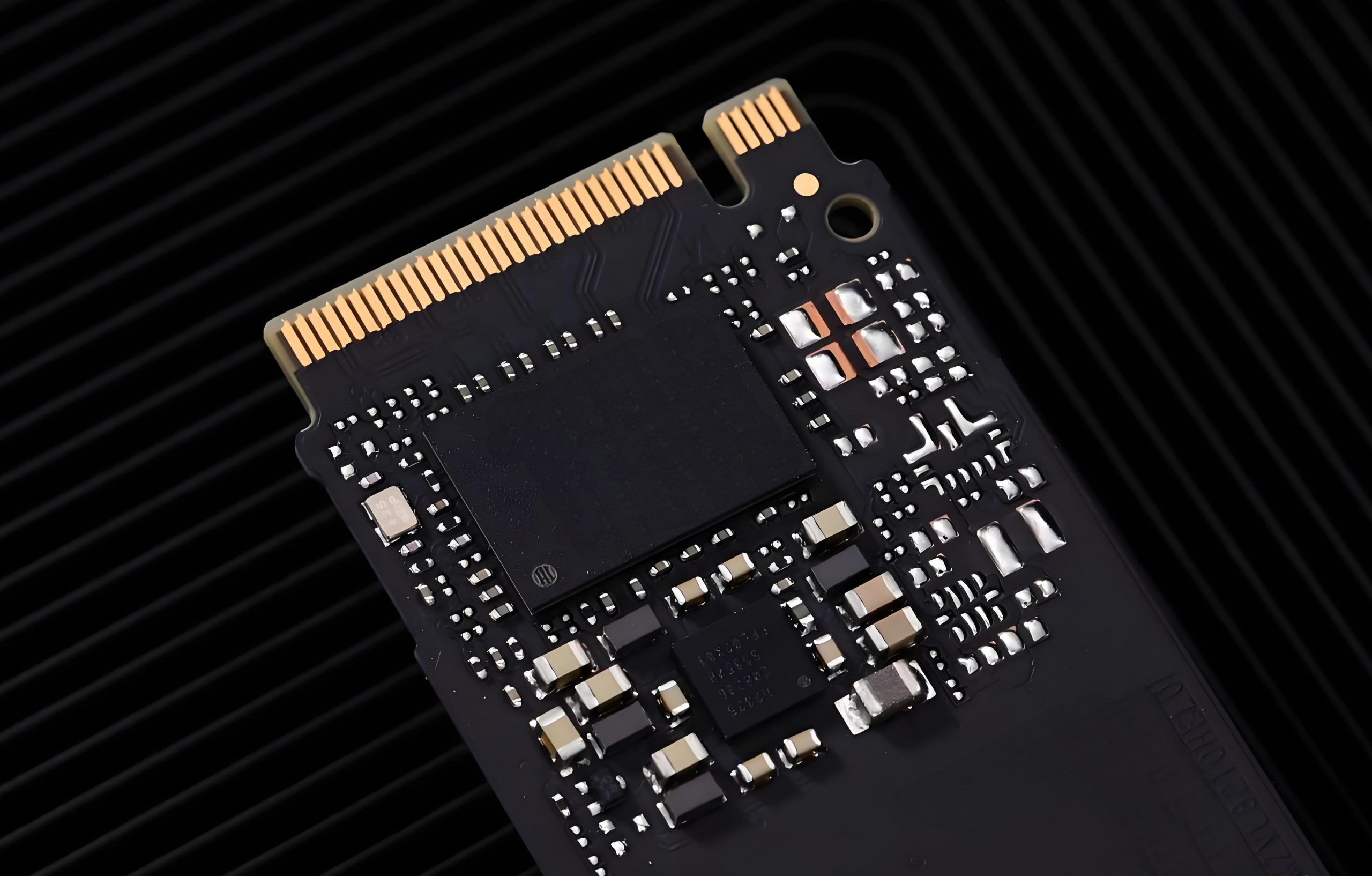
What is SSD PCB?
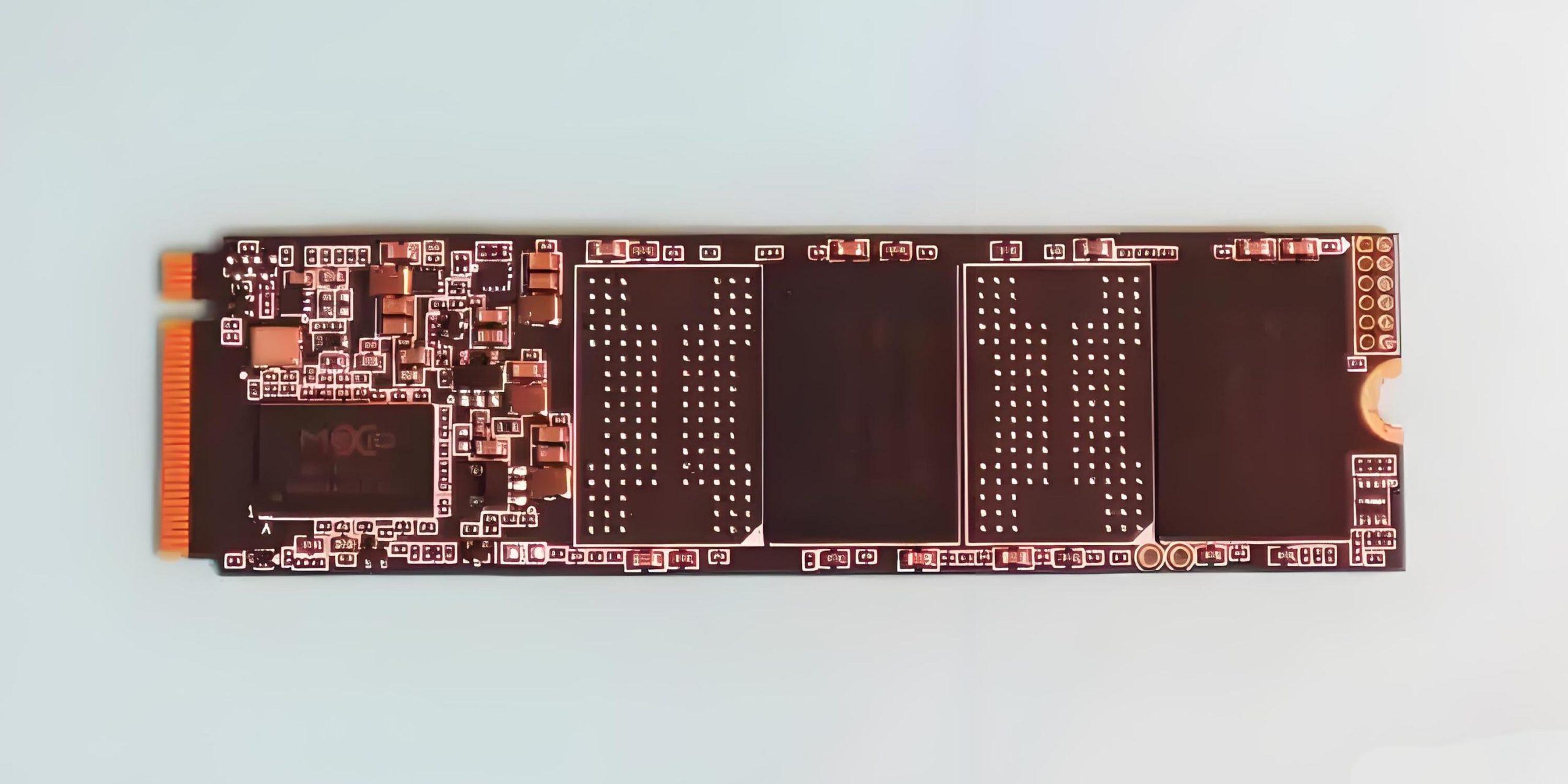
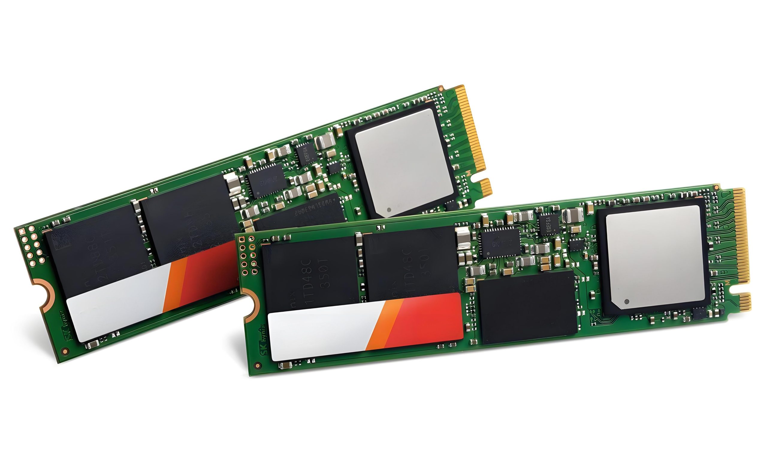
An SSD PCB, or Solid-State Drive Printed Circuit Board, is the backbone of a solid-state drive. It’s the platform that holds the essential components like the flash memory chips, controller, and interface connectors. The PCB provides the electrical pathways that connect these components and ensures smooth communication between them.
At its core, the SSD PCB is what enables the SSD to function as a fast, reliable storage device. Without the proper design and materials, even the best flash memory chips and controllers would not perform optimally.
A well-designed SSD PCB ensures minimal power loss, maximum efficiency, and stable data transfer speeds.
What is SSD PCB design?
SSD PCB design involves creating a blueprint for the SSD’s printed circuit board. This includes selecting the right materials, ensuring optimal routing for electrical signals, managing heat dissipation, and considering layout factors that will allow the SSD to perform at its best.
A good SSD PCB design takes into account factors such as:
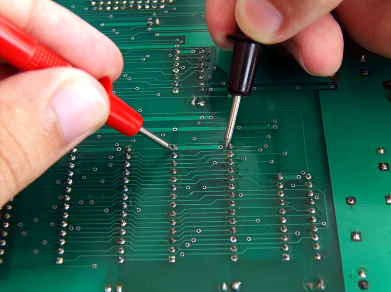
- Electrical Pathways: The routing of signals between memory chips, controllers, and other components is critical. Poor routing can lead to signal interference, which can reduce performance.
- Thermal Management: Poor heat dissipation can lead to overheating, affecting the longevity and reliability of the drive.
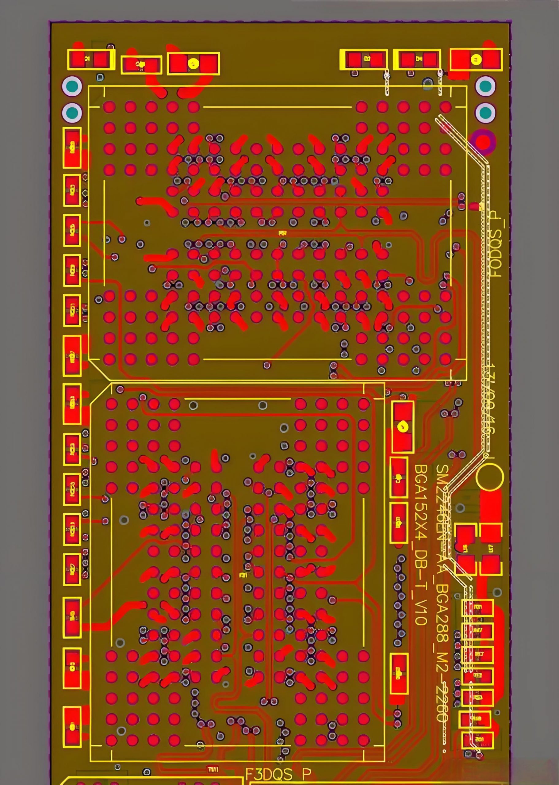
- Component Placement: The arrangement of the components on the PCB impacts the drive’s performance and overall reliability. The design must minimize interference and ensure efficient data flow.
How does PCB design affect SSD speed?
PCB design plays a significant role in determining the speed of an SSD. In fact, the efficiency of the PCB’s layout can make a difference between an average SSD and one that performs at peak speeds.
Proper routing minimizes signal degradation, which is essential for maintaining high-speed data transfer. If the signals are routed inefficiently, delays can occur, slowing down the drive.
Additionally, the use of high-quality PCB materials with low resistance and impedance ensures faster data transfer. The components on the PCB must be placed to avoid interference, and careful design is necessary to keep data access times short and boost read/write speeds.
PCB design: SSD longevity factor?
The longevity of an SSD is another aspect that can be influenced by PCB design. SSDs have a finite number of write/erase cycles due to the nature of flash memory, but good PCB design can help maximize the number of cycles by optimizing power management and ensuring thermal efficiency.
If thermal management is not prioritized in the design, the drive could experience premature failure. Proper heat dissipation allows the components to operate at their optimal temperature, reducing stress on the memory chips and improving the overall lifespan of the drive.
Moreover, optimizing the power delivery system on the PCB helps reduce the wear on the memory chips. Smooth and efficient power distribution ensures that the SSD runs at a steady voltage level, preventing damage to sensitive components.
Why is thermal management critical for SSD PCBs?
SSDs can generate significant heat during operation, especially when performing heavy write operations. If this heat isn’t properly managed, it can cause thermal throttling, where the SSD slows down to prevent damage. In the worst case, excessive heat could lead to component failure and data loss.
To avoid these issues, SSD PCBs are designed with heat sinks, thermal pads, and efficient routing that allow heat to dissipate quickly.
Additionally, using materials with good thermal conductivity ensures that the heat generated by the SSD components is spread out evenly, preventing hot spots.
In high-performance SSDs, effective thermal management can make the difference between optimal performance and premature failure. Therefore, choosing the right PCB materials and layout is essential for maintaining the temperature within acceptable limits.
What is the biggest drawback to SSD drives?
Despite their many advantages, SSDs do have one significant drawback: their limited write endurance. Flash memory in SSDs has a limited number of program/erase cycles. As data is written to and erased from the drive, the memory cells experience wear, which eventually leads to failure.
However, good PCB design can help mitigate this issue by distributing writes evenly across the memory cells. This is done through wear leveling algorithms in the SSD controller. These algorithms ensure that the cells don’t wear out prematurely by spreading data writes across the available memory.
Which lasts longer, HDD or SSD?
In terms of durability and longevity, HDDs (hard disk drives) generally last longer than SSDs in terms of read/write cycles.
However, SSDs offer better performance and reliability in most real-world use cases. While HDDs can be prone to mechanical failures due to moving parts, SSDs, being solid-state, are more resistant to physical shock and damage.
When comparing lifespan, an SSD can endure a few years of heavy usage before the flash memory starts to degrade, while an HDD might last longer under light usage.
What are the best materials for SSD PCBs?
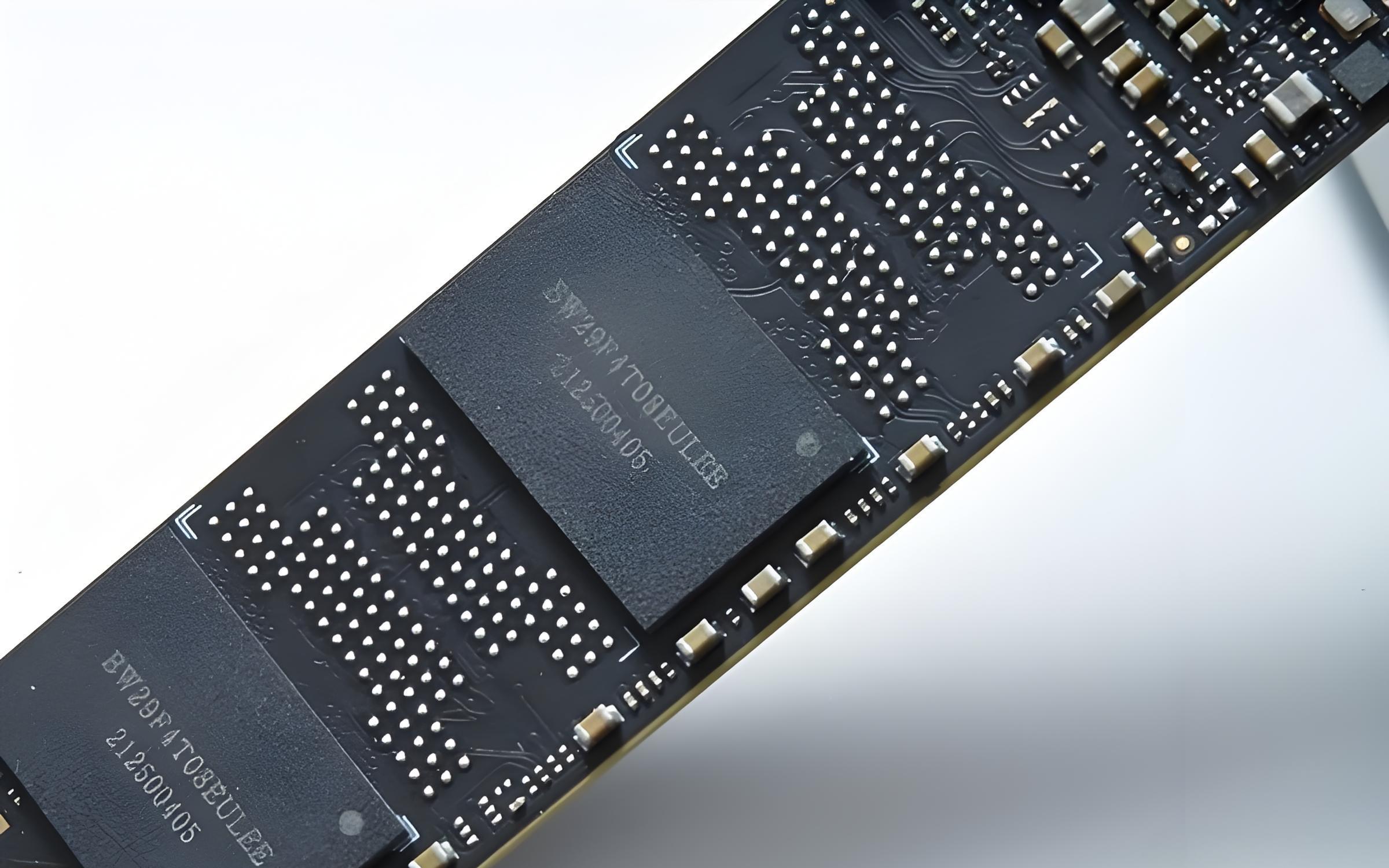
The materials used for SSD PCBs are critical in ensuring both performance and durability. High-quality materials such as FR4, polyimide, and ceramic are commonly used in the production of SSD PCBs.
- FR4: The most commonly used PCB material, FR4 is a fiberglass-based epoxy laminate. It’s affordable and has good electrical insulating properties, making it a standard choice for SSD PCBs.
- Polyimide: Used in flexible and rigid-flexible PCBs, polyimide is a high-performance material with excellent thermal stability and mechanical properties.
- Ceramic: Known for its high thermal conductivity, ceramic is used in some high-end SSD designs to ensure efficient heat dissipation.
In addition to these materials, the selection of high-quality soldering materials and conductive adhesives is essential for ensuring a reliable connection between components.
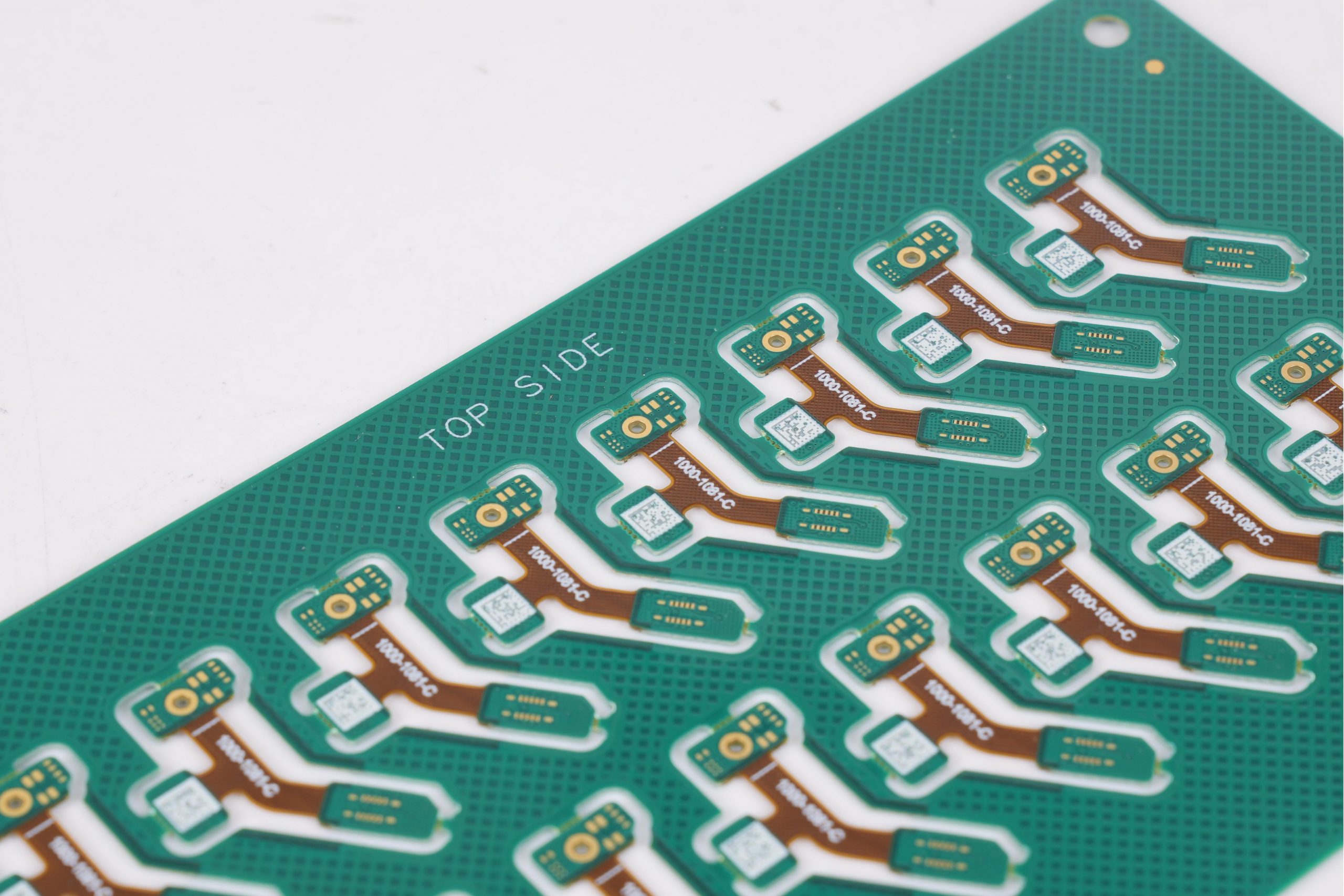
How do multi-layer PCBs benefit SSDs?
Multi-layer PCBs are often used in SSD designs to enhance both performance and density. These PCBs consist of multiple layers of conductive material, allowing for more complex circuit routing without taking up extra space.
Multi-layer PCBs also contribute to thermal management by distributing heat across several layers, reducing the risk of overheating.
Conclusion:
In conclusion, the design of the SSD PCB plays an essential role in determining the drive’s speed, reliability, and longevity. A well-designed SSD PCB ensures optimal performance, efficient thermal management, and long-lasting durability.
For reliable and high-performance SSD PCB design, look no further than EBest Circuit (Best Technology). Our team specializes in designing and manufacturing advanced PCBs tailored to meet the needs of the modern electronic industry. Contact us at sales@bestpcbs.com