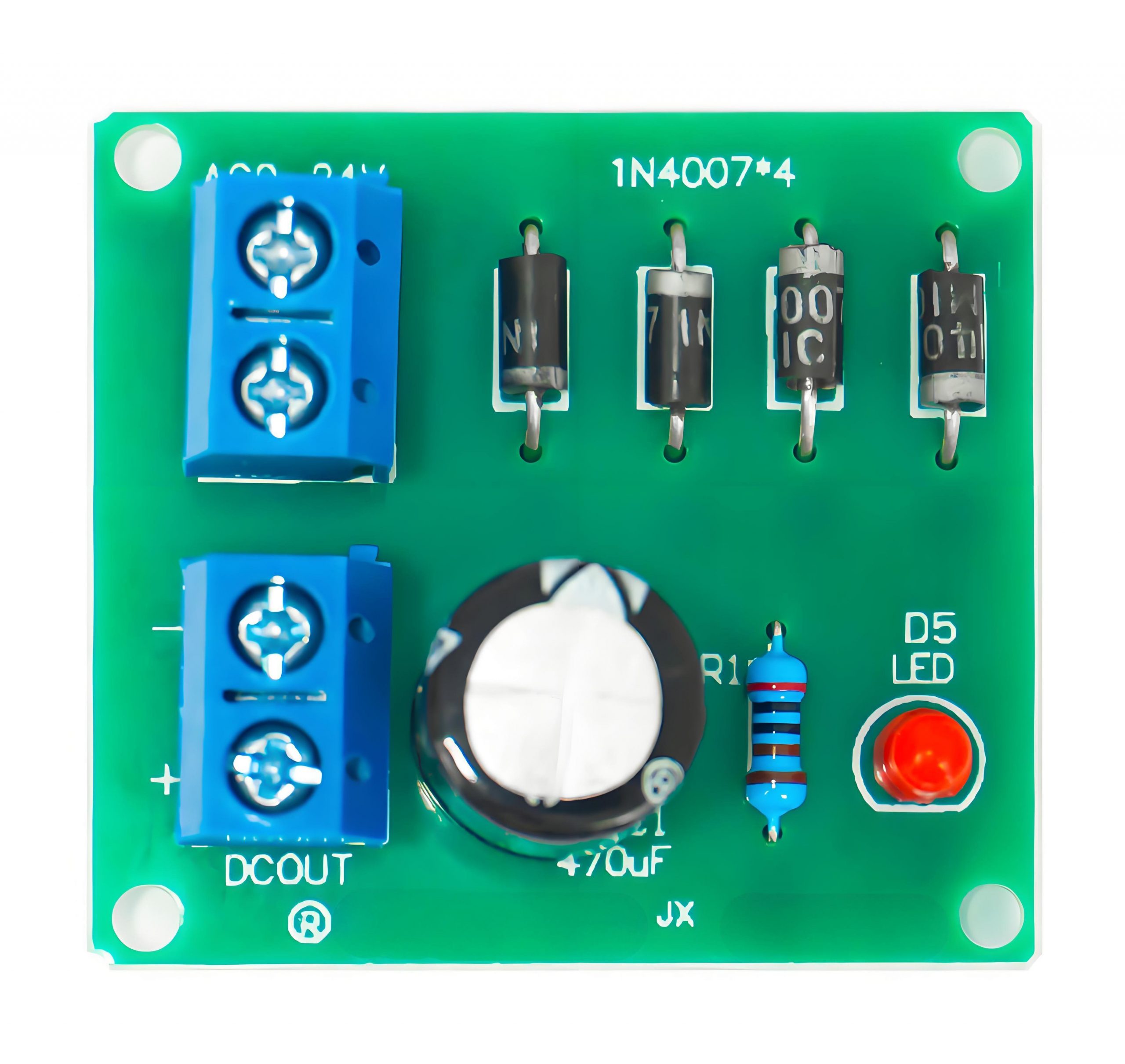
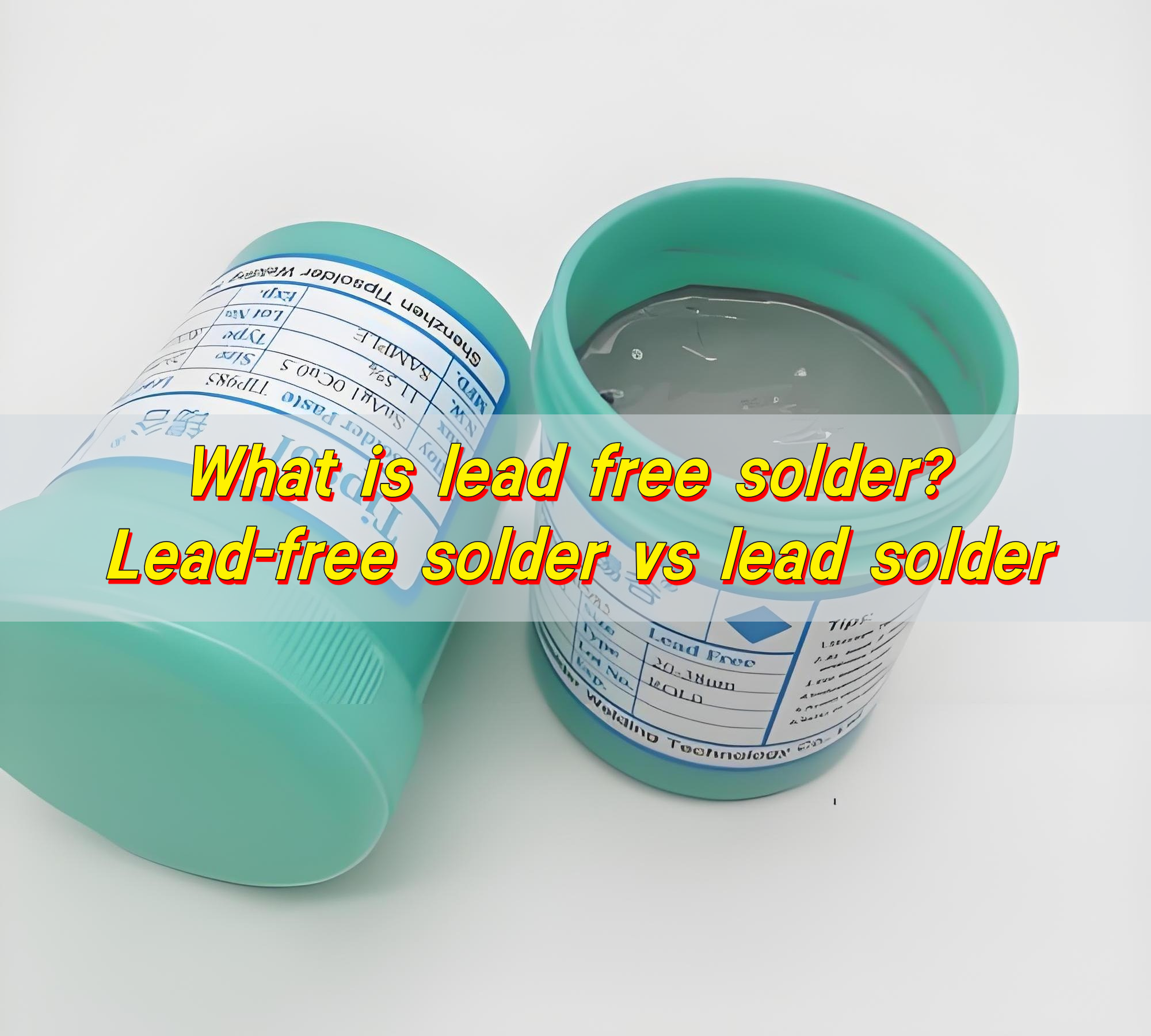
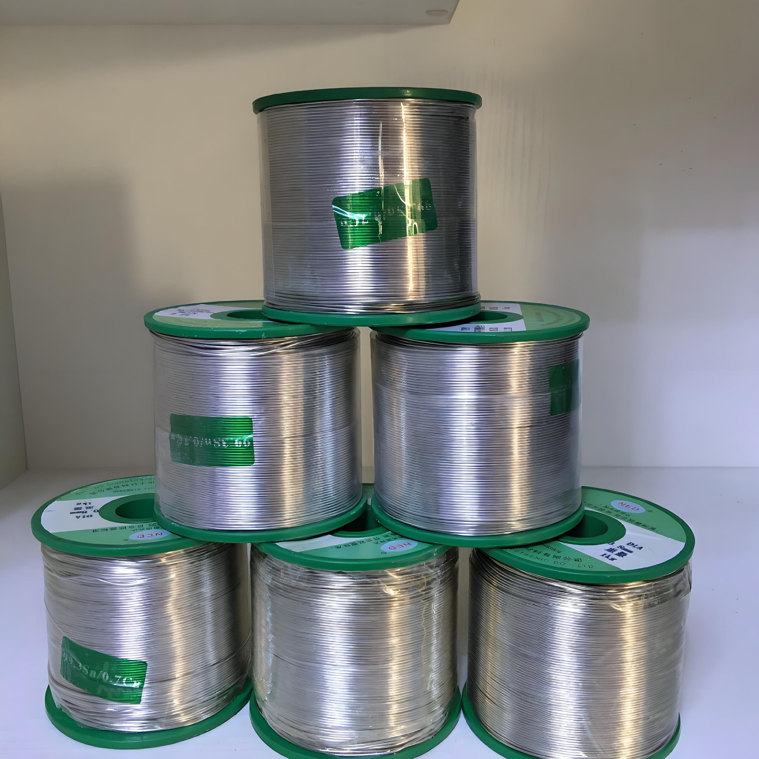
Lead free solder is a welding material that does not contain lead or has a very low lead content. It is mainly composed of metal elements such as tin, silver, and copper, and is used to replace traditional lead-containing solder. It has the characteristics of environmental protection, safety, and reliability, and reduces the harm to the environment and human health.
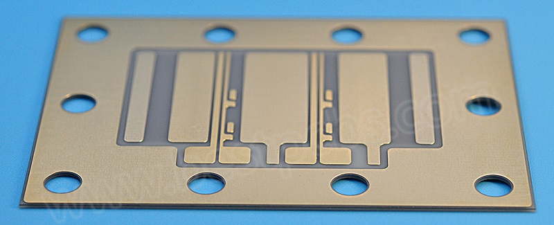
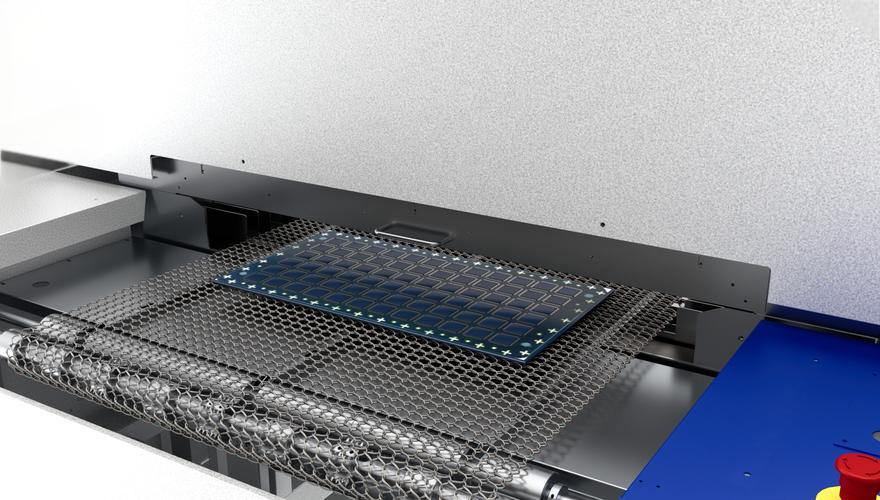
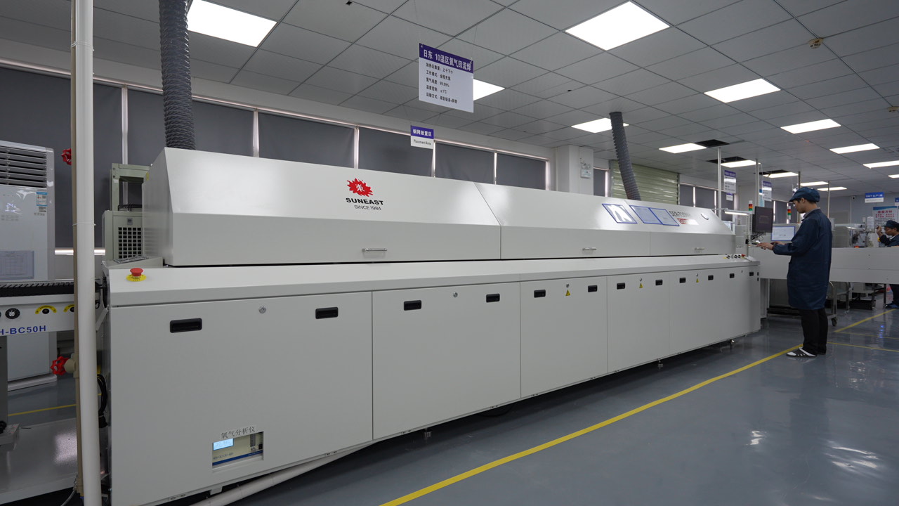
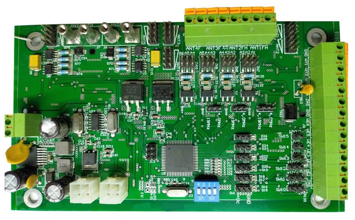
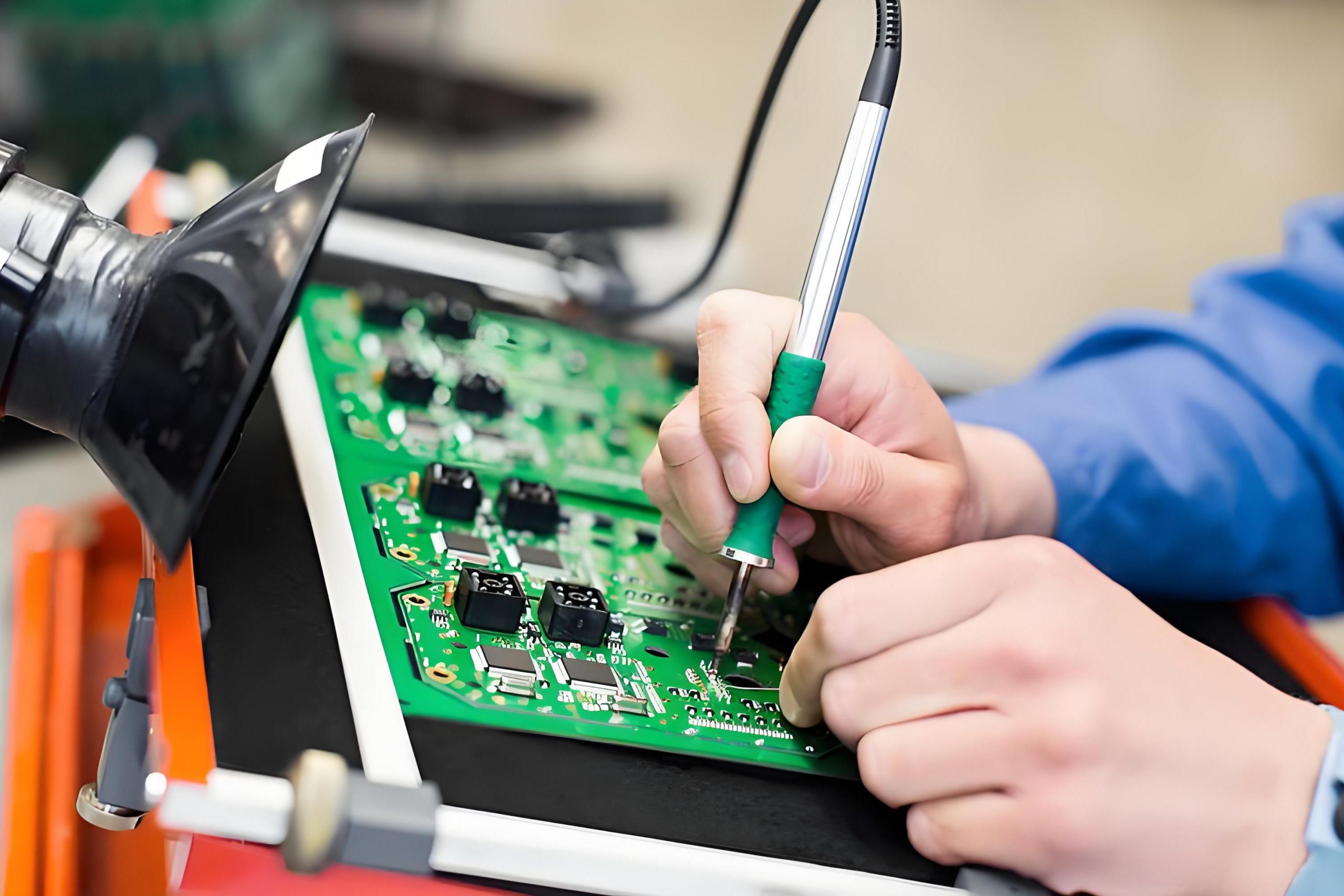
In PCB manufacturing, the use of lead-free solder helps to improve the reliability and durability of products while meeting environmental protection requirements.
What is a lead-free solder?
Lead-free solder refers to a type of solder that doesn’t contain lead. Unlike traditional solder, which is often a blend of lead and tin, lead-free solder typically uses a combination of metals such as tin, silver, and copper.
Lead-free solders are designed to meet environmental and safety regulations, as lead is a toxic substance that can pose serious health risks when it’s exposed to people or the environment.
In simple terms, lead-free solder performs the same task as traditional lead-based solder: it melts and fuses two metal parts together to form a solid electrical connection. The key difference lies in the composition of the material itself.
With the growing demand for safer alternatives, particularly in electronics manufacturing, lead-free solder has risen to prominence.
What is the downside of lead-free solder?
Lead-free solder generally requires higher temperatures to melt compared to traditional lead-based solder. This can lead to potential issues during the soldering process, especially for components that are sensitive to heat.
Another challenge is the difference in workability. Lead-free solder tends to be a bit more difficult to work with because it has a higher viscosity, which means it doesn’t flow as smoothly as leaded solder. This can make it harder to achieve clean, precise solder joints, especially when using manual soldering techniques.
What is lead free solder made of?
Lead-free solder is primarily composed of tin (Sn), but it also contains other metals like silver (Ag), copper (Cu), bismuth (Bi), and sometimes indium (In) or zinc (Zn). The specific mix of metals varies depending on the exact type of lead-free solder used.
Commonly used lead-free solder alloy is a mixture of 96.5% tin, 3% silver, and 0.5% copper, often referred to as SAC305. This particular alloy is favored in electronics manufacturing due to its reliable performance and low risk of corrosion.
Other variations of lead-free solder may include bismuth or indium to lower the melting point or improve the flow characteristics. The choice of materials largely depends on the application and the specific requirements of the soldering process.
Why is lead not used in solder anymore?
The shift away from lead in solder is driven by health and environmental concerns. Lead is a toxic heavy metal that can cause serious health problems, especially when it is ingested or inhaled. Ingesting even small amounts of lead over time can result in lead poisoning, which can affect the nervous system, kidneys, and other organs.
As a result, organizations like the European Union and the Environmental Protection Agency (EPA) have put regulations in place that limit the use of lead in products like electronics and plumbing. These regulations, such as the RoHS Directive (Restriction of Hazardous Substances), require manufacturers to use alternatives to lead in many products, including solder.
Which is better, lead or lead-free solder?
The debate between lead and lead-free solder depends largely on the specific needs of the user. Lead-free solder has clear benefits in terms of health and environmental safety, especially when it comes to meeting regulations like RoHS.
However, lead-based solder is still preferred by some for certain applications because it has a lower melting point, which makes it easier to work with.
For general-purpose use, lead-free solder is often the better choice, particularly in industries where safety and compliance are top priorities.
However, for high-performance or delicate components, lead-based solder might still have the edge due to its superior ease of use, lower temperature requirements, and better flow characteristics.
What is the best lead-free solder?
There isn’t a single “best” lead-free solder because the right choice depends on your specific application. However, some of the most commonly used lead-free solder alloys include:
- SAC305 (96.5% Tin, 3% Silver, 0.5% Copper): This is a popular choice in electronics and provides a good balance of mechanical strength and resistance to thermal cycling.
- SAC405 (96% Tin, 4% Silver): Often used in more demanding applications, SAC405 has a slightly higher silver content, which can improve performance in high-temperature environments.
- SnCu (99.3% Tin, 0.7% Copper): This solder is often used in applications where cost is a concern, as it’s cheaper than alloys that contain silver.
The “best” lead-free solder will depend on the specific requirements of your project, including the types of components being soldered, the temperature range, and other factors like workability and durability.
What does 60/40 mean in solder?
The 60/40 ratio refers to a blend of 60% tin and 40% lead, which is the classic composition for traditional lead-based solder. This mixture has been the standard for many years due to its relatively low melting point and excellent workability.
However, with the rise of lead-free solder for environmental and safety reasons, the 60/40 solder is being phased out in favor of safer alternatives.
What temp does lead free solder melt?
The melting point of lead-free solder depends on the specific alloy used. In general, most lead-free solders have a melting temperature that is higher than lead-based solder. For instance, SAC305 has a melting point of around 217-221°C (423-430°F), while traditional 60/40 lead-based solder melts at around 183°C (361°F).
This difference means that soldering with lead-free solder often requires higher temperatures and may need more careful temperature control to prevent overheating and damaging components.
Does lead free solder need flux?
Yes, lead-free solder requires flux to ensure that the solder adheres properly to the surfaces being joined and to remove any oxides or impurities.
Flux is essential in both lead and lead-free soldering, but it’s especially important when using lead-free solder. The higher melting temperatures and different composition of lead-free alloys make it even more crucial to use the right type of flux.
Flux helps to reduce the surface tension of the solder, allowing it to flow more easily and create strong, reliable connections. It also prevents the formation of oxides during the heating process, which could affect the quality of the solder joint.
Conclusion:
Lead-free solder is a safer, more environmentally friendly alternative to traditional lead-based solder. While it comes with certain challenges—such as higher melting temperatures and slightly more difficult workability—the benefits in terms of health and regulatory compliance make it the go-to choice in modern manufacturing.
If you need help selecting the best lead-free solder for your project or have questions about PCB assembly, don’t hesitate to reach out to us at sales@bestpcbs.com. We’re happy to assist you with all your soldering and PCB needs.