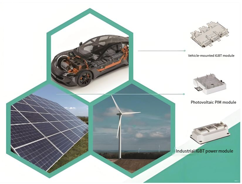
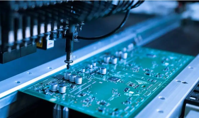
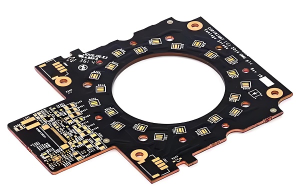
When it comes to precision engineering and high-quality manufacturing, Germany stands at the forefront globally. The German PCB (Printed Circuit Board) industry is a shining example of this excellence, renowned for its commitment to innovation, reliability, and adherence to strict quality standards. Serving critical sectors such as automotive, industrial automation, medical technology, and aerospace, German PCB manufacturers are trusted partners for businesses worldwide seeking top-tier circuit solutions. In this comprehensive guide, we will delve into the landscape of the German PCB industry, highlighting the top 10 PCB manufacturers in Germany and providing expert insights to help you navigate the process of selecting the ideal German PCB manufacturer for your specific needs.
Top 10 PCB Manufacturers in Germany Detailed List
Below is an overview of ten leading PCB manufacturing companies in Germany, each excelling in technical capabilities, production scale, and market reputation.
| Company Name | Core Process Capabilities | Key Strengths | Headquarters Location |
|---|---|---|---|
| AT&S Austria Technologie & Systemtechnik | High-end HDI PCBs, IC substrates, RF PCBs, embedded component technology | Global leader in semiconductor packaging substrates, expert in automotive electronics | Leoben, Austria (Group headquarters with significant operations in Germany) |
| TT Electronics (formerly Schweizer Electronic) | High-layer count PCBs, thick copper PCBs, hybrid dielectric PCBs, flexible PCBs | Leader in industrial and medical applications, strong R&D and customization capabilities | Heppenheim |
| Zollner Elektronik | Complex PCB assemblies, system integration, cable assemblies | One of Europe’s largest Electronic Manufacturing Services (EMS) providers, one-stop solutions | Pfullingen |
| Elbe Holding (including Elbe Print GmbH) | Double-sided and multi-layer PCBs, aluminum PCBs, high-frequency PCBs, rapid prototyping | Comprehensive technology portfolio, flexible service, deep customer base in automotive and industry | Hamburg |
| PCB Piezotronics Europe GmbH (German branch) | Specialized PCBs for sensors and actuators | Unique expertise in piezoelectric technology and sensor integration | Schweinfurt |
| Medico PCB GmbH | Medical device-specific PCBs, high-reliability PCBs, small-batch customization | Focus on medical sector, strict adherence to ISO 13485 and other medical industry standards | Berlin |
| Circuit Systems GmbH | Multi-layer PCBs, HDI, flexible and rigid-flex PCBs, rapid prototyping | Technologically advanced, innovation-driven, serving industrial, automotive, and communication sectors | Munich |
| Pro2 Electronics GmbH | PCB manufacturing, electronic assembly, testing, and logistics services | Full EMS services from prototype to production, high flexibility | Dresden |
| Eurocircuits Deutschland GmbH | Prototype and small-batch PCB manufacturing, standard and specialty materials | Convenient online quoting and ordering system, serving European engineers and startups | Dortmund |
| Mitteldeutsche Leiterplatten GmbH (MLP) | Double-sided and multi-layer PCBs, high Tg materials, metal-core PCBs | Based in central Germany, serving local and regional industrial customers | Halle |
How to Select the Right PCB Manufacturer in Germany
Choosing an ideal PCB manufacturer is a critical step for the success of your product. With numerous excellent German manufacturers available, you can evaluate them based on the following core dimensions:
1. Clarify Your Requirements and Match Manufacturer’s Technical Capabilities
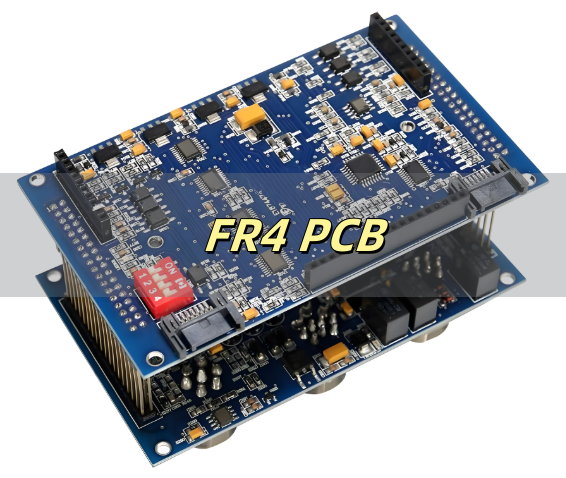
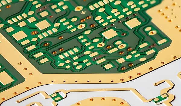
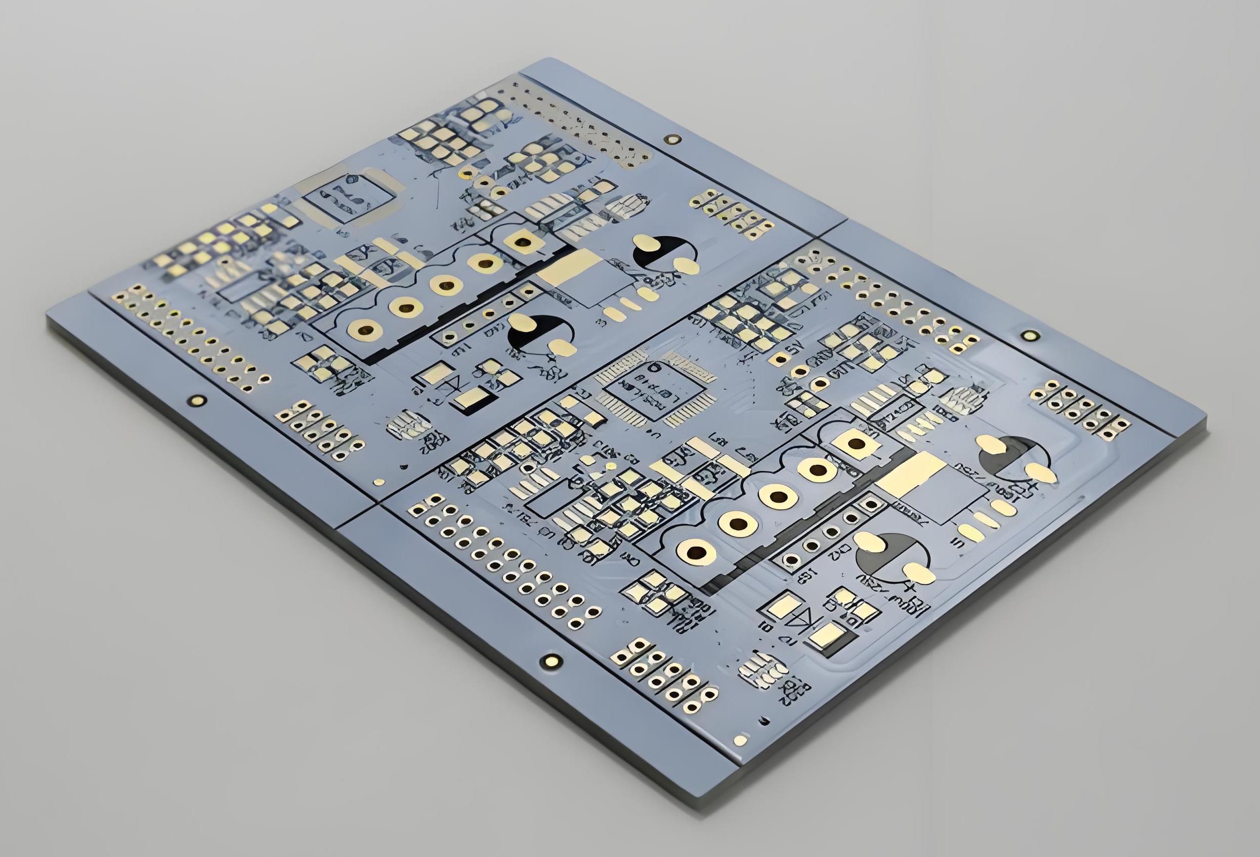
- Board Type: Do you need standard FR-4 multi-layer boards, HDI boards, flexible PCBs (FPC), rigid-flex PCBs, aluminum substrates, or special PCBs made from high-frequency/high-speed materials?
- Technical Parameters: Layer count, minimum line width/space, minimum via diameter, board thickness, surface finish, etc., must match the manufacturer’s process capabilities.
- Application Field: Different sectors like automotive, medical, and industrial control have varying standards and requirements (e.g., UL certification, ISO 13485). Ensure the manufacturer has relevant experience and qualifications.
2. Evaluate Manufacturer’s Production Capacity and Quality System
- Capacity and Lead Time: Can the manufacturer’s monthly production capacity meet your current and future order demands? What are the standard lead times and expedited service options?
- Quality Certifications: Is the manufacturer ISO 9001 certified? Are industry-specific certifications (like IATF 16949 for automotive) available?
- Testing Capabilities: Does the manufacturer have comprehensive incoming, in-process, and final inspection capabilities, such as AOI (Automated Optical Inspection), X-Ray inspection, and flying probe testing?
3. Consider Cost-Effectiveness and Supply Chain Stability
- Quotation Transparency: Is the quotation clear and comprehensive, including all costs (e.g., engineering fees, testing fees, tooling costs)?
- Payment Terms: Are there flexible payment options available?
- Supply Chain Management: Does the manufacturer have stable raw material suppliers? In case of material shortages, are there alternative plans and risk mitigation strategies?
4. Value Communication and Service Support
- Technical Support: Can the manufacturer provide DFM (Design for Manufacturability) advice during the design phase to optimize PCB design and improve yield?
- Communication Efficiency: Are the sales and technical teams responsive and professional?
- After-Sales Service: Is there a clear process and warranty for handling quality issues?
Core Pain Points Analysis of PCB Manufacturers in Germany
Despite their strong capabilities, German PCB manufacturers face several common challenges in the current global market environment.
- High Operational Costs: Sustained high labor, energy, and land costs in Germany directly compress profit margins, making it difficult to compete on price with manufacturers from low-cost Asian countries.
- Intense International Competition: PCB giants from China, South Korea, and Taiwan pose significant pressure on German manufacturers in the global mid-to-low-end and even some high-end markets, leveraging economies of scale and cost advantages.
- Raw Material Price Volatility and Supply Risks: Prices of key raw materials like copper and copper-clad laminates are subject to fluctuations in the international commodity markets. Meanwhile, geopolitical tensions and global supply chain instability threaten the stable supply of raw materials.
- Shortage of Technical Talent: The manufacturing industry, particularly the PCB sector requiring highly specialized skills, faces a shortage of skilled technicians and experienced engineers, limiting innovation and expansion.
- Pressure from Rapid Technological Iteration: Electronic technology evolves rapidly, constantly raising performance requirements for PCBs (e.g., higher frequency, faster speed, smaller size). Manufacturers need continuous substantial investment in equipment upgrades and R&D to keep pace with technological advancements.
- Stringent Environmental Regulations: Germany and the EU have some of the world’s strictest environmental regulations. PCB manufacturing involves various chemicals that can pollute the environment if not properly handled. Manufacturers must invest heavily in environmental protection facilities and operations to ensure compliance.
- Challenges of Low-Volume, High-Mix Production: The European local market often demands low-volume, high-mix, and customized products, which contradicts large-scale, standardized production models. This places higher requirements on production line flexibility and rapid changeover capabilities, increasing production complexity.
How to Evaluate the Production Capacity of German PCB Manufacturers
Accurately assessing the true production capacity of a PCB manufacturer is crucial to ensuring high-quality, on-time delivery of your orders.
- Assess Factory Scale and Equipment Advancement: Understand the size and layout of production facilities, as well as the brand, model, and quantity of key production equipment (e.g., drilling machines, exposure machines, etching machines, plating lines, AOI equipment). Advanced equipment is the foundation for ensuring process precision and stability.
- Audit Quality System Certifications: Request to see ISO 9001, IATF 16949, and other quality system certificates. Further investigate internal quality control processes and key performance indicators (KPIs) such as yield rates and customer complaint rates.
- Evaluate R&D Investment and Technological Innovation Capabilities: Understand the annual R&D investment ratio, the presence of an in-house R&D team, and the number of patents or successful cases in new technologies and processes. This reflects the enterprise’s long-term competitiveness.
- Verify Capacity Data and Delivery Records: Request data on monthly production capacity and maximum single-batch production capacity. More importantly, reference past delivery records and customer reviews to judge actual delivery capability and reliability.
- Examine Supply Chain Management Capabilities: Inquire about the list of major raw material suppliers, procurement processes, inventory management strategies, and emergency plans for material shortages. A stable supply chain is essential for continuous production.
- Conduct Sample Testing and Small-Batch Trial Production: Before formal mass production, prototype and small-batch trial production can directly verify the manufacturer’s process level, quality control capabilities, and production collaboration.
- Understand Customer Structure: Observe the main customer groups. Serving well-known, quality-demanding large companies (especially in automotive or medical fields) indirectly confirms production capacity and quality standards.
How to Evaluate the Lead Time of German PCB Manufacturers
On-time delivery is critical for many projects. Evaluating the reliability of lead times from German PCB manufacturers can be approached from the following aspects:
- Clarify Standard Delivery Cycles: Consult the manufacturer on standard production and delivery cycles for different types and batches of PCB products. This serves as a baseline reference.
- Inquire About Expedited Service Possibilities and Conditions: Understand if expedited production services are available in emergencies, the expedited cycle time, and the calculation of expedited fees.
- Analyze Production Planning and Scheduling Systems: Advanced Advanced Planning and Scheduling (APS) systems help manufacturers arrange production more efficiently, reduce waiting times, and improve on-time delivery rates.
- Assess Order Processing Workflow: Efficiency in each link, from order confirmation and engineering file review to material procurement and formal production, affects the final delivery date. Understand if internal processes are smooth and efficient.
- Evaluate Capacity Utilization Rate: Factories operating at long-term full capacity are likely to have extended lead times for new orders. Gauge current production busyness through communication and industry insights.
- Understand Logistics Partners and Solutions: PCB products typically require safe and fast logistics. Assess the reliability of logistics partners and the existence of comprehensive packaging and transportation plans to ensure timely and intact delivery.
- Reference Historical Customer Reviews: Request customer references or research industry forums and social media to understand past customer experiences with delivery reliability.
- Specify Delivery Terms in Contracts: Clearly define delivery dates and liability for delayed delivery in contracts to constrain manufacturers and protect your interests.
Major Challenges Facing the German PCB Industry
From a macro perspective, the German and broader European PCB industries face several structural challenges.
- Global Industrial Chain Restructuring and Regionalization Trends: Geopolitical conflicts, trade frictions, and post-pandemic reflections on supply chain security are driving the global industrial chain toward regionalization and localization. This presents opportunities for German PCB manufacturers to serve the local market while requiring enhanced integration capabilities within the regional supply chain.
- Persistent Cost Pressures: As mentioned earlier, high labor, energy, and raw material costs are long-term challenges for the German PCB industry. Continuously addressing these costs through technological innovation and lean production is an ongoing task.
- Talent Drain and Skills Shortages: Manufacturing’s appeal to younger generations is declining due to factors like salary levels and working environments. Simultaneously, experienced technicians and managers are approaching retirement, challenging the industry’s overall skill level.
- Increasingly Stringent Environmental Protection and Sustainability Requirements: EU policies like the “Green Deal” impose higher demands on manufacturing carbon footprints, resource recycling, and chemical usage. As a potentially polluting industry, the PCB sector needs increased investment in green transformation to achieve sustainable development.
- Competitive Pressure from Asian Manufacturers: Asian PCB manufacturers hold significant advantages in capacity, cost, and rapid response, dominating the global market. German and European manufacturers must find core competitiveness in technological differentiation, high quality, customized services, and local support.
- Mismatch Between Technological Innovation Speed and Market Demand: While Germany leads in high-end manufacturing technology, rapidly changing market demands and emerging applications (e.g., AI, IoT, new energy vehicles) require quick industry response and adaptation to avoid technological leadership without market relevance.
- Uncertainty in Geopolitics and International Trade Policies: Changes in trade policies such as tariff barriers and export controls may impact the international business expansion and supply chain stability of German PCB manufacturers, increasing operational risks.
Conclusion
With its profound technical accumulation, rigorous quality control, and innovative spirit, the German PCB manufacturing industry occupies a unique and important position in the global market, particularly excelling in high-end sectors like automotive electronics, industrial control, and medical devices. Choosing the right German PCB manufacturer means securing high-quality products and professional service guarantees. We hope this list of the top 10 PCB manufacturers in Germany and the accompanying analysis provide valuable references for your procurement decisions. In practice, we recommend conducting a comprehensive, detailed evaluation based on your specific needs to establish a stable, long-term partnership.