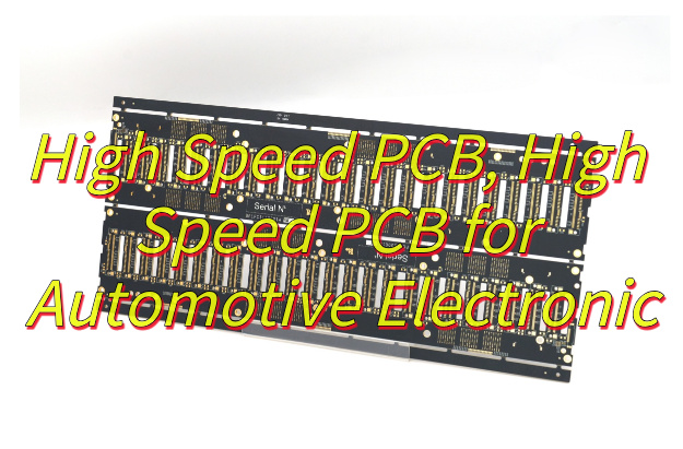
Looking for RF PCB solutions? This guide explores its 4-layer stackup, frequency ranges, grounding best practices, and smart logistics applications for AGVs and real-time data.
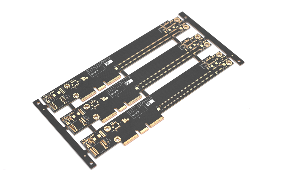
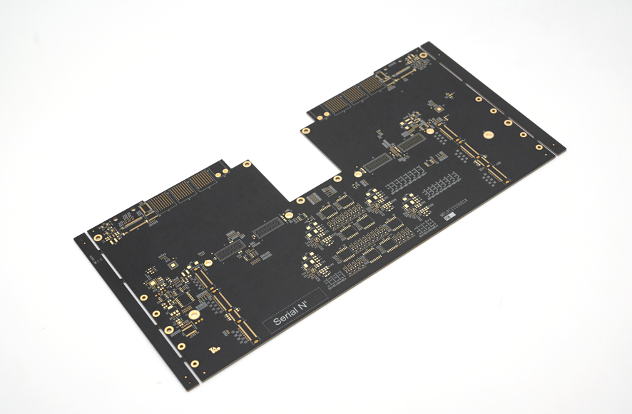
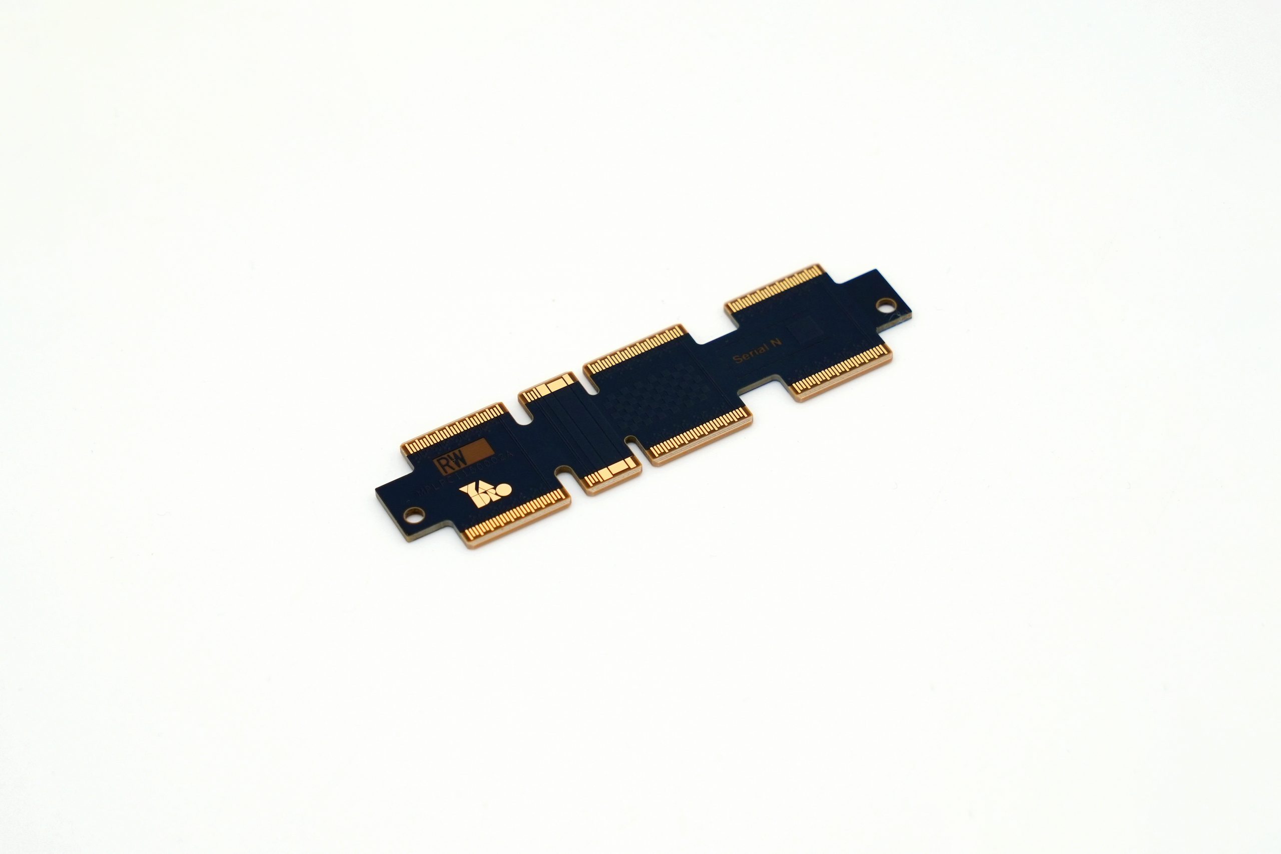
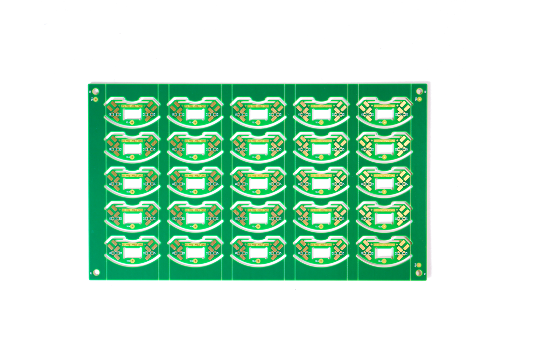
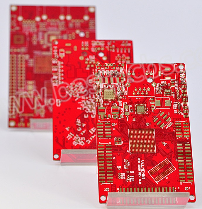
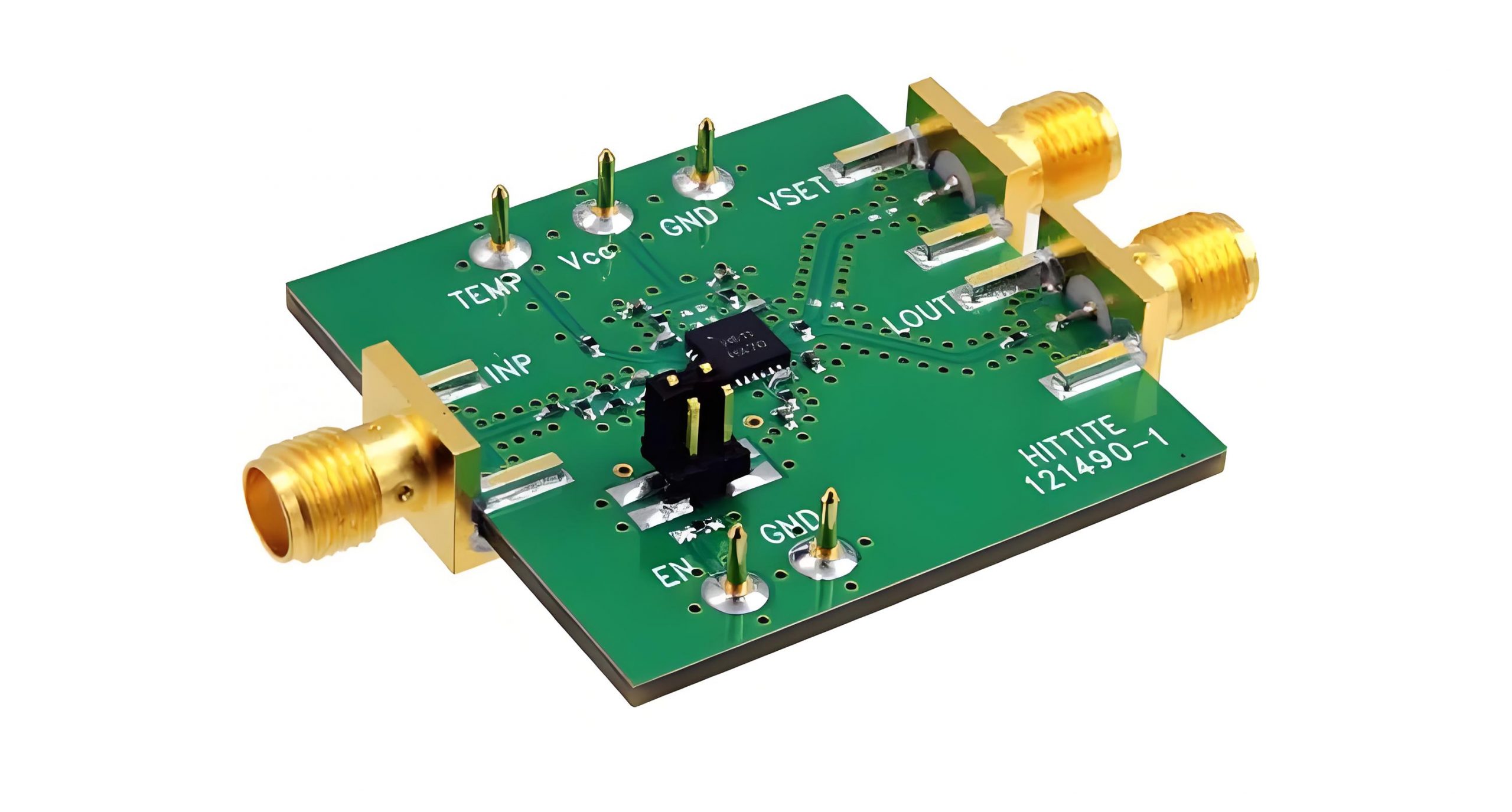
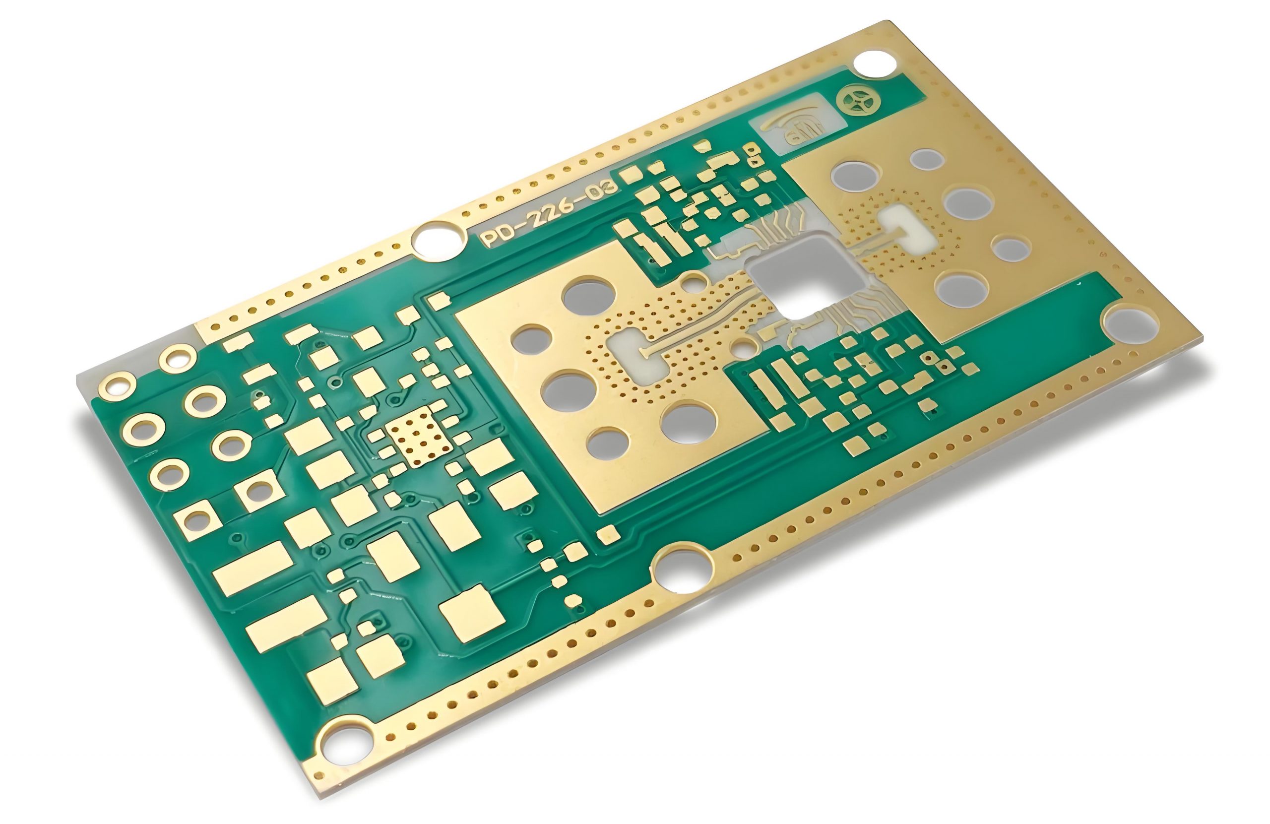
EBest Circuit (Best Technology) stands out as a premier RF PCB manufacturer for intelligent logistics by delivering unmatched speed, precision, and reliability. Our rapid 15-day lead time ensures timely deployment of RFID and AGV systems, minimizing downtime in warehouse automation. With ISO-certified production and 99.98% defect-free rate, we guarantee signal integrity even in high-frequency 5.8GHz operations through advanced impedance control (+/- 3%). Our proprietary 4-layer hybrid stackup combines Rogers 4350B and FR-4 materials, achieving optimal RF performance while reducing costs by 18%. The company’s 0.1mm laser-drilled microvias enable compact antenna designs for real-time inventory tracking, cutting labor costs by 30% in smart warehouses. Rigorous HAST testing ensures seamless AGV navigation in harsh industrial environments. Welcome to contact us: sales@bestpcbs.com.
What Is RF PCB?
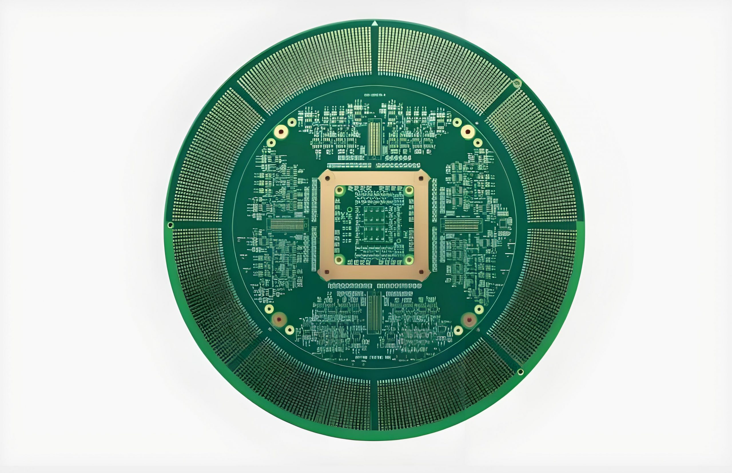
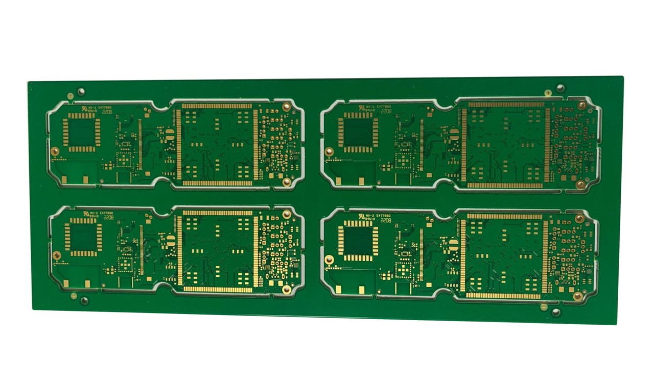
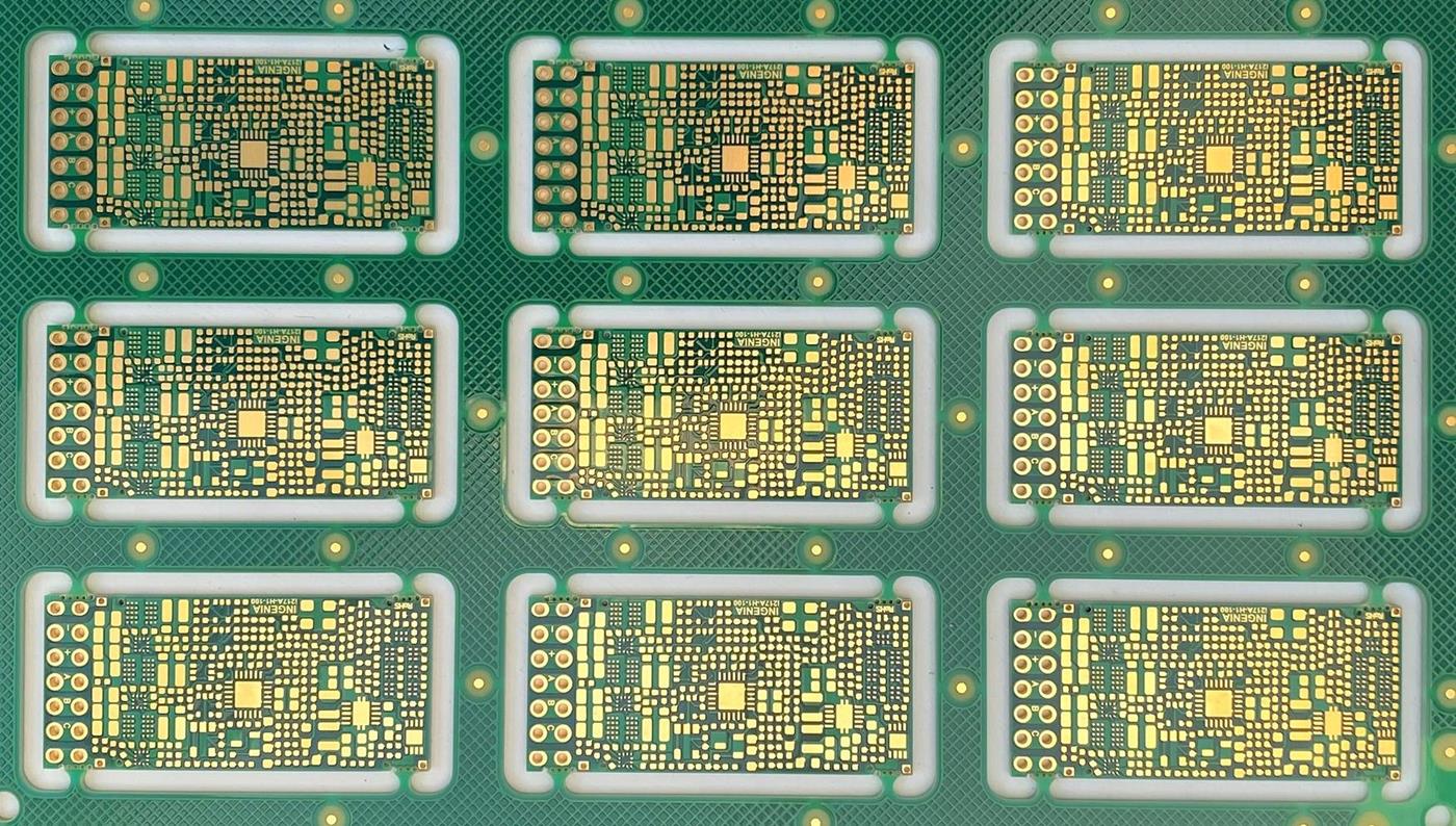
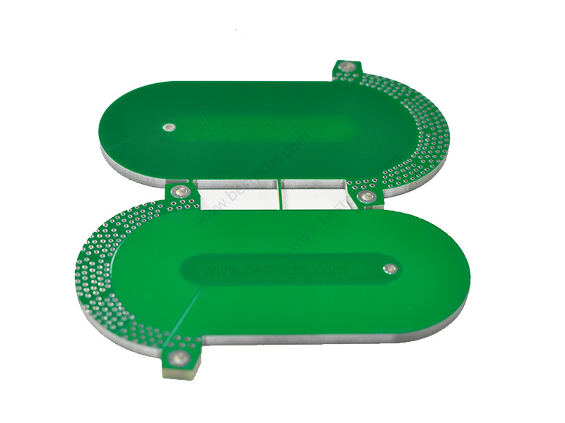
A RF PCB, or radio frequency printed circuit board, serves as the fundamental hardware platform specifically engineered to manage high-frequency signals essential for wireless communication in automated systems. Unlike standard circuit boards, a RF PCB demands specialized materials and meticulous layout techniques to maintain signal integrity at microwave frequencies, ensuring reliable data transmission between devices like RFID readers, sensors, and tracking modules within warehouses or distribution centers. This unique capability allows the RF PCB to form the operational core of intelligent logistics networks, enabling real-time asset tracking, autonomous inventory management, and environmental monitoring without constant manual intervention. Consequently, deploying robust RF PCB designs directly contributes to labor efficiency in logistics automation by minimizing physical checks, reducing error corrections, and supporting seamless machine-to-machine coordination across the supply chain.

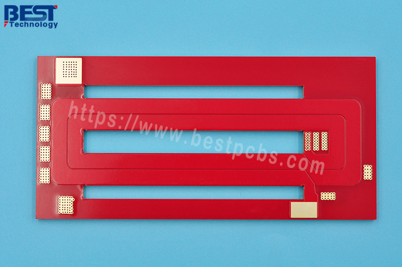
What Is Stackup Structure of 4 Layer RF PCB?
Below is stackup structure of 4 layer RF PCB:
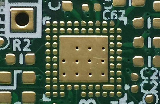
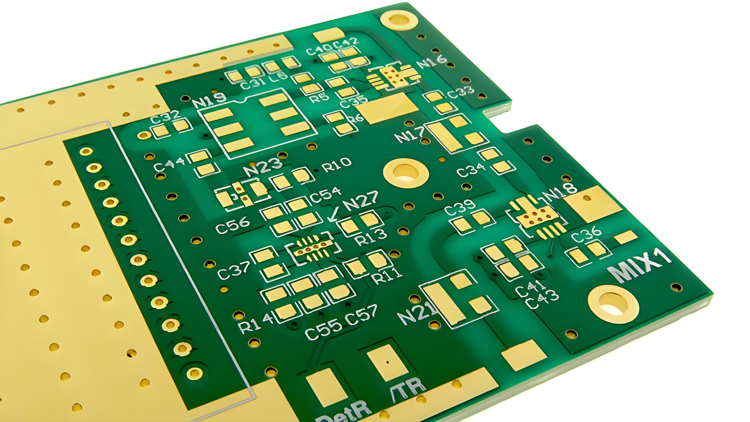
- Top Layer (Signal Layer): This layer primarily hosts RF traces, antennas, and high-frequency components. Traces here require precise impedance control, often set to 50 ohms for RF applications. The layout prioritizes short trace lengths to reduce signal loss. For RF PCB boards in intelligent logistics, this layer directly interfaces with wireless modules like antennas or transceivers.
- Inner Layer 1 (Ground Plane): Positioned beneath the top layer, this layer serves as a continuous ground reference. It minimizes electromagnetic interference by providing a low-impedance return path for RF signals. A solid ground plane here enhances shielding and reduces parasitic inductance, critical for maintaining signal clarity in RF PCB designs.
- Inner Layer 2 (Power Plane): Dedicated to power distribution, this layer isolates DC power from sensitive RF signals. It often includes decoupling capacitors placed near power-hungry components to filter noise. For RF PCB boards, this layer ensures stable power delivery while acting as an additional EMI shield.
- Bottom Layer (Auxiliary Signal Layer): The bottom layer handles lower-speed signals, control lines, or non-RF components. It may also incorporate ground pours to improve thermal dissipation and mechanical stability. In intelligent logistics applications, this layer might support interfaces like UART, SPI, or GPIO for peripheral devices.
What Is the Frequency Range Supported by the RF PCBs?
The frequency range an RF PCB (Radio Frequency Printed Circuit Board) supports directly impacts its suitability for intelligent logistics applications. Below is a detailed breakdown of common frequency bands and their practical relevance:
Standard RF Bands (500 MHz – 6 GHz)
- Applications: This range covers most wireless technologies used in logistics, including Wi-Fi, Bluetooth, Zigbee, and cellular networks (4G/LTE/5G).
- Use Case: RF PCB boards in this range power RFID readers, warehouse IoT gateways, and handheld scanners. For example, 2.4 GHz is ubiquitous in short-range communication devices.
Millimeter-Wave Frequencies (6 GHz – 30 GHz)
- Applications: Advanced RF PCB boards may operate here to support high-speed data links or radar systems.
- Use Case: In logistics, this range enables ultra-wideband (UWB) precision tracking or collision-avoidance sensors in autonomous vehicles.
Material-Driven Performance Limits
- High-Performance Substrates: Materials like PTFE or ceramic composites allow RF PCB boards to function reliably up to 30 GHz, making them ideal for demanding applications.
- Cost-Effective Options: FR4-based boards typically max out below 6 GHz due to signal loss at higher frequencies but remain suitable for simpler logistics tools.
Logistics-Specific Frequency Allocation
- Sub-1 GHz (e.g., 433 MHz, 868 MHz): Used for low-power, long-range RFID tags and environmental sensors spanning large facilities.
- 2.4 GHz & 5 GHz: Standard for Wi-Fi/Bluetooth-enabled devices like inventory drones or worker wearables.
- 24 GHz: Emerges in logistics for short-range radar applications, such as detecting obstacles in automated guided vehicles (AGVs).
Design Choices Affecting Frequency Coverage
- Impedance Matching: Precise 50-ohm trace design ensures minimal signal reflection across all frequencies.
- Layer Optimization: A four-layer RF PCB board isolates high-frequency traces on the top layer while using inner layers for ground/power planes.
- Shielding Techniques: Ground planes and via stitching reduce electromagnetic interference (EMI), critical for maintaining signal integrity.
What Are the Best Practices For RF PCB Ground Wiring?
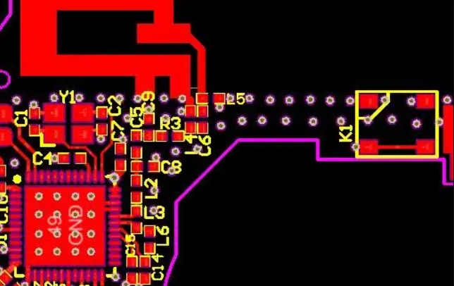
- Prioritize Solid Ground Planes: Begin by allocating dedicated layers for continuous ground planes. These planes act as low-impedance return paths for RF signals, reducing electromagnetic interference (EMI) and crosstalk. Avoid splitting ground planes unless absolutely necessary, as gaps can create inductive loops and disrupt signal return paths. In multi-layer boards, stack the ground plane adjacent to the RF signal layer to minimize loop areas.
- Strategically Place Ground Vias: Use arrays of stitched ground vias to connect ground planes across layers. This technique lowers inductance and ensures a uniform ground potential. Position vias near RF components, connectors, and high-speed signal traces. For example, placing vias every 50-100 mils along RF transmission lines helps anchor the ground return path and prevents resonant modes.
- Isolate Analog and Digital Grounds: In mixed-signal RF designs, such as those integrating Bluetooth Low Energy (BLE) or Wi-Fi modules with microcontrollers, segregate analog and digital ground domains. Connect these domains at a single point—typically under the power supply or a dedicated grounding pad—to prevent digital noise from coupling into sensitive analog circuits. Use ferrite beads or inductors at the junction if high-frequency noise is a concern.
- Minimize Loop Areas for Critical Traces: Route RF traces over continuous ground planes to shrink current loop areas. Smaller loops reduce susceptibility to external magnetic fields and radiated emissions. For differential pairs, maintain equal trace lengths and symmetric spacing relative to the ground plane to preserve signal balance.
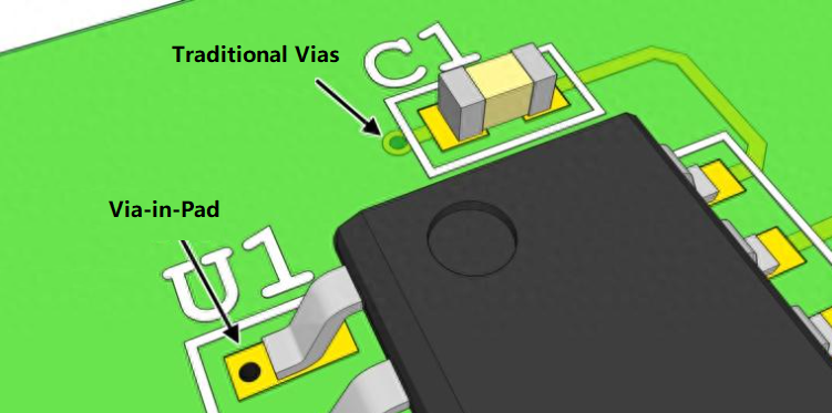
- Optimize Component Grounding: Surface-mount components with via-in-pad or thermal relief connections to the ground plane. This reduces lead inductance and improves thermal dissipation. For RF connectors, ensure their ground pins make direct contact with the ground plane without intervening traces or components.
- Implement Guard Rings and Shielded Inductors: Surround vulnerable RF traces or components with guard rings—narrow copper traces connected to the ground plane. These rings absorb stray fields and shield against EMI. Use shielded inductors in RF circuits to mitigate magnetic coupling between adjacent components.
- Control Impedance with Ground Returns: Match the impedance of RF traces to the system requirements (e.g., 50 ohms for many RF applications) by adjusting trace width, dielectric thickness, and proximity to the ground plane. Use co-planar waveguide (CPW) structures with ground strips adjacent to the signal trace for tighter impedance control in dense layouts.
- Distribute Decoupling Capacitors Effectively: Place high-frequency decoupling capacitors close to RF power pins. Connect their ground terminals directly to the ground plane via short, wide traces to minimize inductance. For multi-layer boards, embed capacitors in the same layer as the RF components to shorten current paths.
- Avoid Sharp Bends in Ground Traces: Use 45-degree angles instead of 90-degree bends for ground traces and RF signal routes. Sharp bends create impedance discontinuities and increase radiation. Similarly, avoid acute angles in ground pour connections to prevent EMI hotspots.
- Validate with Thermal and EMI Simulations: Before finalizing the design, simulate thermal performance to ensure ground planes dissipate heat efficiently, especially in compact logistics devices. Use EMI simulation tools to identify and mitigate ground bounce or resonance issues. Post-fabrication, test with near-field probes to confirm ground integrity and signal quality.
Why Choose RF PCB Boards for Intelligent Logistics?
Here’s why RF PCB boards are the ideal choice for intelligent logistics:
- Enhanced Signal Integrity in Complex Environments: Logistics facilities often involve dense equipment, metal structures, and moving machinery—all of which can disrupt wireless signals. RF PCB boards are engineered to minimize signal loss and interference, ensuring consistent communication between devices like asset trackers, scanners, and IoT sensors. This reliability reduces downtime and operational delays.
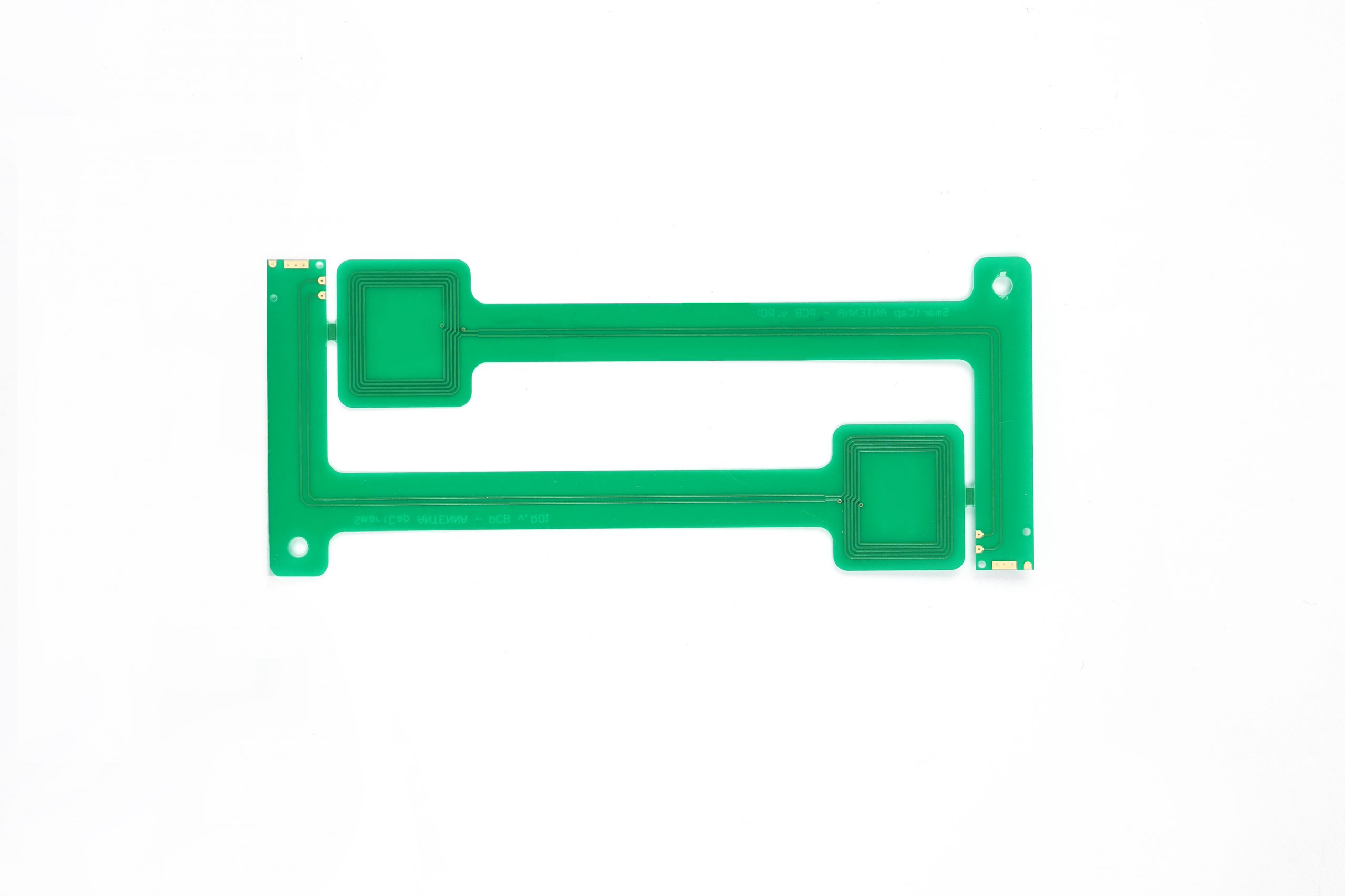
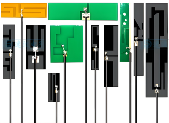
- Compact Design for Space-Constrained Applications: Many logistics devices, such as handheld scanners, wearable trackers, and in-vehicle routers, require compact hardware. RF PCB boards integrate antennas, filters, and impedance-matched traces into a small footprint, enabling sleek, ergonomic designs without compromising performance.
- Durability for Harsh Logistics Conditions: Logistics environments expose equipment to vibrations, temperature fluctuations, and rough handling. RF PCB boards use robust materials and construction techniques to withstand these stresses. For example, immersion gold finishes prevent corrosion, while thick copper traces resist wear from repeated use.
- Energy Efficiency for Battery-Powered Devices: Many logistics tools, such as wireless sensors and mobile terminals, rely on batteries. RF PCB boards optimize power usage by reducing signal loss and enabling low-power communication protocols like Bluetooth Low Energy (BLE) or Zigbee. This extends battery life, reducing maintenance costs and downtime.
- Scalability for Growing Operations: As logistics networks expand, adding new devices or upgrading infrastructure becomes inevitable. RF PCB boards support modular designs, allowing easy integration of emerging technologies like 5G, ultra-wideband (UWB), or AI-driven analytics. This adaptability protects your investment in hardware.
- Cost-Effective Long-Term Performance: While RF PCB boards may have a higher upfront cost compared to standard PCBs, their durability and efficiency reduce long-term expenses. Fewer repairs, longer device lifespans, and lower energy consumption translate to measurable savings over time.
- Compliance with Industry Standards: Logistics operations often require adherence to regulations like FCC, CE, or RoHS. RF PCB boards are designed to meet these standards, ensuring your devices can operate globally without compliance hurdles.
- Customization for Specialized Needs: Every logistics workflow has unique requirements. RF PCB manufacturers offer customizable solutions, from layer stack-ups and impedance control to embedded antennas and shielding. This flexibility ensures your hardware perfectly matches your operational demands.
How Can RF PCB Designs Cut Labor Costs in Smart Logistics Systems?
- Automate Inventory Management with Reliable Sensors: RF PCB-powered sensors enable real-time tracking of assets, packages, and vehicles. By eliminating the need for manual stock checks or location verification, these systems reduce labor hours spent on inventory audits. For example, RFID tags with integrated antennas on PCBs ensure accurate, automatic updates, freeing staff for higher-value tasks.
- Enable Predictive Maintenance: RF PCBs in IoT devices monitor equipment health—such as conveyor belts, forklifts, or sorting machines—by transmitting performance data wirelessly. Algorithms analyze this data to predict failures before they occur, allowing maintenance teams to address issues proactively. This reduces emergency repairs and the labor costs associated with unexpected downtime.
- Simplify Device Deployment and Calibration: Compact, modular RF PCB designs simplify the installation of wireless nodes, gateways, and access points. Pre-calibrated PCB modules with embedded antennas reduce the time technicians spend on setup and tuning. For instance, plug-and-play RF modules in warehouses cut deployment labor by up to 40% compared to manual wiring.
- Improve Warehouse Navigation for Robots: RF PCBs in autonomous guided vehicles (AGVs) and drones enable precise indoor positioning using technologies like UWB or Wi-Fi 6. Accurate navigation reduces the need for human supervisors to guide robots, lowering labor costs while increasing throughput.
- Centralize Control with Wireless Networks: RF PCB-based mesh networks create self-healing wireless infrastructure, eliminating the need for extensive cabling and manual network management. Technicians can monitor and adjust settings remotely, reducing site visits and on-site labor.
- Enhance Worker Safety Through Automation: RF PCB designs in safety systems—such as collision-avoidance sensors or emergency stop triggers—reduce the risk of accidents. Fewer incidents mean less labor spent on injury management, training, and compliance audits.
- Scale Operations Without Proportional Labor Growth: Modular RF PCB architectures allow logistics firms to expand their wireless infrastructure incrementally. Adding new devices or coverage areas requires minimal manual configuration, enabling businesses to grow without linearly increasing their workforce.
- Reduce Training Time with Intuitive Hardware: Standardized RF PCB designs simplify device operation and maintenance. Unified interfaces and diagnostic tools reduce the time needed to train staff on new equipment, lowering labor costs associated with onboarding and skill gaps.
How Does RF PCB Durability Ensure Seamless AGV Integration in Intelligent Logistics?
- Robust Material Selection for Longevity: High-TG (glass transition temperature) laminates and ceramic-filled substrates resist thermal expansion and mechanical fatigue, common in AGVs subjected to constant movement and vibrations. These materials prevent solder joint cracks and trace delamination, extending PCB lifespan.
- Enhanced Coating for Environmental Resistance: Apply conformal coatings—such as parylene or acrylic—to shield RF PCBs from dust, moisture, and chemicals present in warehouse environments. This protection prevents corrosion and short circuits, reducing maintenance needs.
- Optimized Layer Stack-Up for Stress Distribution: Multi-layer PCBs with staggered via arrays and thick copper cores distribute mechanical stress evenly across the board. This design minimizes the risk of fractures in AGVs navigating uneven floors or encountering obstacles.
- Vibration-Damping Mounting Solutions: Secure RF PCBs within AGVs using rubber grommets or shock-absorbing fasteners. These dampeners mitigate vibrations from motors, wheels, or collisions, preserving solder joints and component integrity.
- Redundant Grounding Paths for Reliability: Incorporate multiple ground vias and stitching capacitors to create redundant low-impedance paths. This ensures consistent signal return even if one path fails, maintaining communication between AGVs and central control systems.
- High-Power Handling for Motor Control: Thick copper traces and embedded heat sinks in RF PCBs manage the thermal loads from AGV motors and power converters. This prevents overheating during prolonged operation, such as continuous towing or lifting tasks.
- EMI Shielding for Uninterrupted Navigation: Encase sensitive RF components, like GPS modules or LiDAR interfaces, in metal cans or conductive enclosures. This shielding blocks electromagnetic interference from nearby machinery or wireless networks, ensuring precise navigation.
- Modular Design for Easy Replacement: Partition RF PCBs into functional modules—such as communication, sensing, and power units—with standardized connectors. This allows quick replacement of damaged sections, minimizing AGV downtime.
- Rigorous Testing for Real-World Conditions: Subject RF PCBs to accelerated life testing, including thermal cycling, vibration profiling, and humidity exposure. Simulate years of AGV operation in weeks to identify and rectify weaknesses before deployment.
- Predictive Maintenance Through Embedded Sensors: Integrate RF PCBs with temperature sensors and voltage monitors to track performance metrics in real time. Analytics platforms can flag deviations, enabling proactive maintenance and preventing sudden failures.
Can Optimized RF PCB Production Accelerate Real-Time Data Flow for Intelligent Logistics?
Yes, optimized RF PCB production can significantly accelerate real-time data flow in intelligent logistics systems. By streamlining manufacturing processes, enhancing quality control, and integrating advanced design features, RF PCBs become more reliable, efficient, and tailored to the demands of fast-paced logistics operations. Below is a detailed analysis of how this optimization drives tangible benefits:
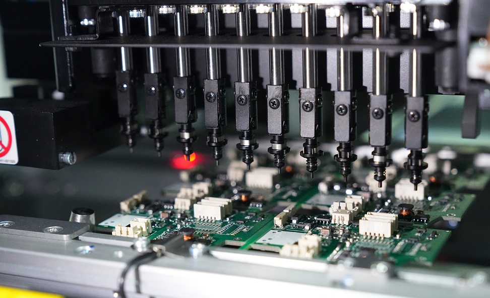
- Automated Production for Faster Turnaround: Advanced manufacturing techniques, such as automated pick-and-place machines and laser drilling, reduce production time while maintaining precision. This rapid turnaround ensures logistics providers can deploy RF-enabled devices—like real-time trackers or IoT gateways—quickly, minimizing delays in scaling their operations.
- Precision Testing Ensures Signal Integrity: Rigorous in-line testing during production, including impedance measurements and EMI scans, identifies defects early. This reduces the risk of faulty PCBs reaching the field, which could cause data transmission errors or latency in logistics networks.
- High-Quality Materials for Consistent Performance: Using premium substrates and copper cladding enhances PCB durability and electrical performance. For example, low-loss dielectric materials minimize signal attenuation, ensuring data packets reach their destination faster in wireless sensor networks or AGV communication systems.
- Compact Designs Free Up Space for Additional Features: Optimized layer stacking and miniaturized components allow RF PCBs to include more functionality in less space. This enables logistics devices to integrate additional sensors, antennas, or processors without increasing form factor, supporting faster data aggregation and processing.
- Environmental Resistance Reduces Downtime: Production processes that incorporate conformal coatings or immersion gold finishes protect PCBs from moisture, dust, and temperature swings. Fewer failures in harsh environments mean fewer interruptions to real-time data streams, such as location updates or inventory alerts.
- Scalable Manufacturing for Growing Demands: Flexible production lines that adapt to varying order volumes ensure logistics companies can expand their RF device fleets as needed. Whether deploying 100 or 10,000 units, optimized production maintains quality and speed, supporting real-time data flow at any scale.
- Customization for Specialized Logistics Needs: Tailored RF PCB designs, such as those with embedded antennas or multi-protocol support (e.g., Wi-Fi 6, Bluetooth 5.3), align with specific logistics workflows. This customization eliminates compatibility issues and accelerates data exchange between diverse systems, like warehouses, trucks, and retail outlets.
- Predictive Analytics in Production: Leveraging data from PCB testing phases allows manufacturers to predict and resolve potential bottlenecks. For instance, identifying a recurring defect in a batch enables real-time adjustments, preventing delays that could ripple through logistics supply chains.
- Streamlined Supply Chains for Component Sourcing: Optimized production includes robust supplier networks that ensure timely access to critical components, such as high-frequency capacitors or RF connectors. This reduces lead times and prevents shortages that could halt logistics device production.
- Training and Collaboration for Seamless Integration: Manufacturers that work closely with logistics providers during PCB design and production ensure the final product aligns with operational needs. This collaboration reduces rework and accelerates deployment, enabling real-time data systems to go live faster.
Conclusion
In summary, for intelligent logistics systems requiring high-frequency stability (5.8GHz), EBest Circuit (Best Technology) delivers RF PCBs with 15-day lead times and 99.98% reliability. Our 4-layer stack-ups with hybrid Rogers/FR-4 materials reduce signal loss by 40%, while laser-drilled 0.1mm microvias enable compact antenna designs that improve inventory tracking accuracy. AGV-compatible boards undergo HAST testing (130°C/85%RH) for harsh environments. Contact EBest Circuit (Best Technology) for RF PCB quotes that optimize your logistics costs: sales@bestpcbs.com.