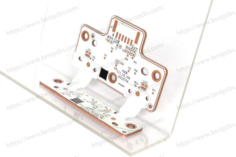
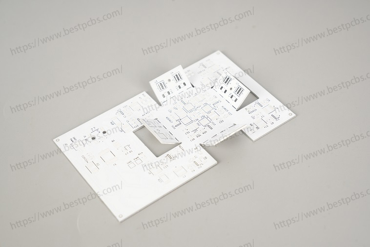
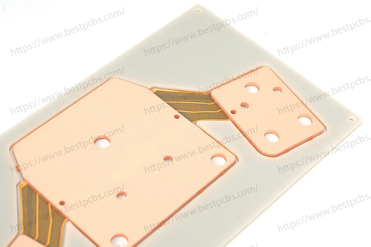
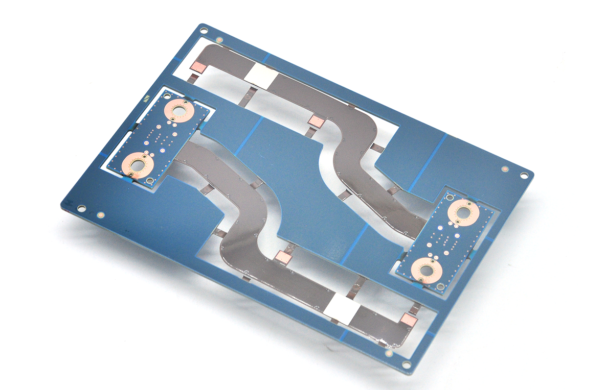
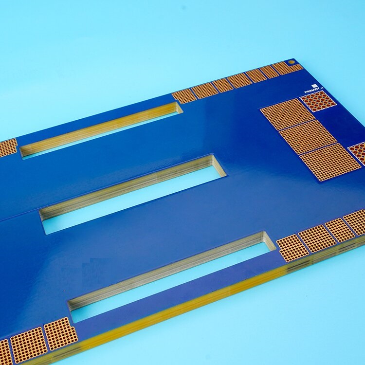
With the continuous growth of new energy demand and the transformation of energy structure, the market size of high-power technology continues to expand. The high power pcb includes heavy copper pcb, bus bar pcb. As an important part of the battery module in the energy storage system, the high power PCB plays a key role in the safety and performance of the entire system. This article explores key considerations when designing high power PCBs, providing insights to help you optimize your designs for demanding applications.
How Important is Thermal Management in High Power PCB Design?
Thermal management is crucial in high power PCB design to prevent overheating and ensure reliable operation. High power components generate significant heat, which can damage the PCB and reduce its lifespan if not managed effectively. Here are some key strategies:
- Use thicker copper layers to improve thermal conductivity as much as possible. For example, a 2 oz/ft² copper layer can carry approximately 10 amps of current.
- Thermal Vias are important elements in the complex designs, they serve as the heat dissipation paths to conduct heat away from high power components.
- Select appropriate heat sinks based on the power dissipation requirements. For instance, a heat sink with a thermal resistance of 1°C/W can handle 50W of power dissipation with a 50°C temperature rise.
How to Optimize Power Distribution in High Power PCBs?
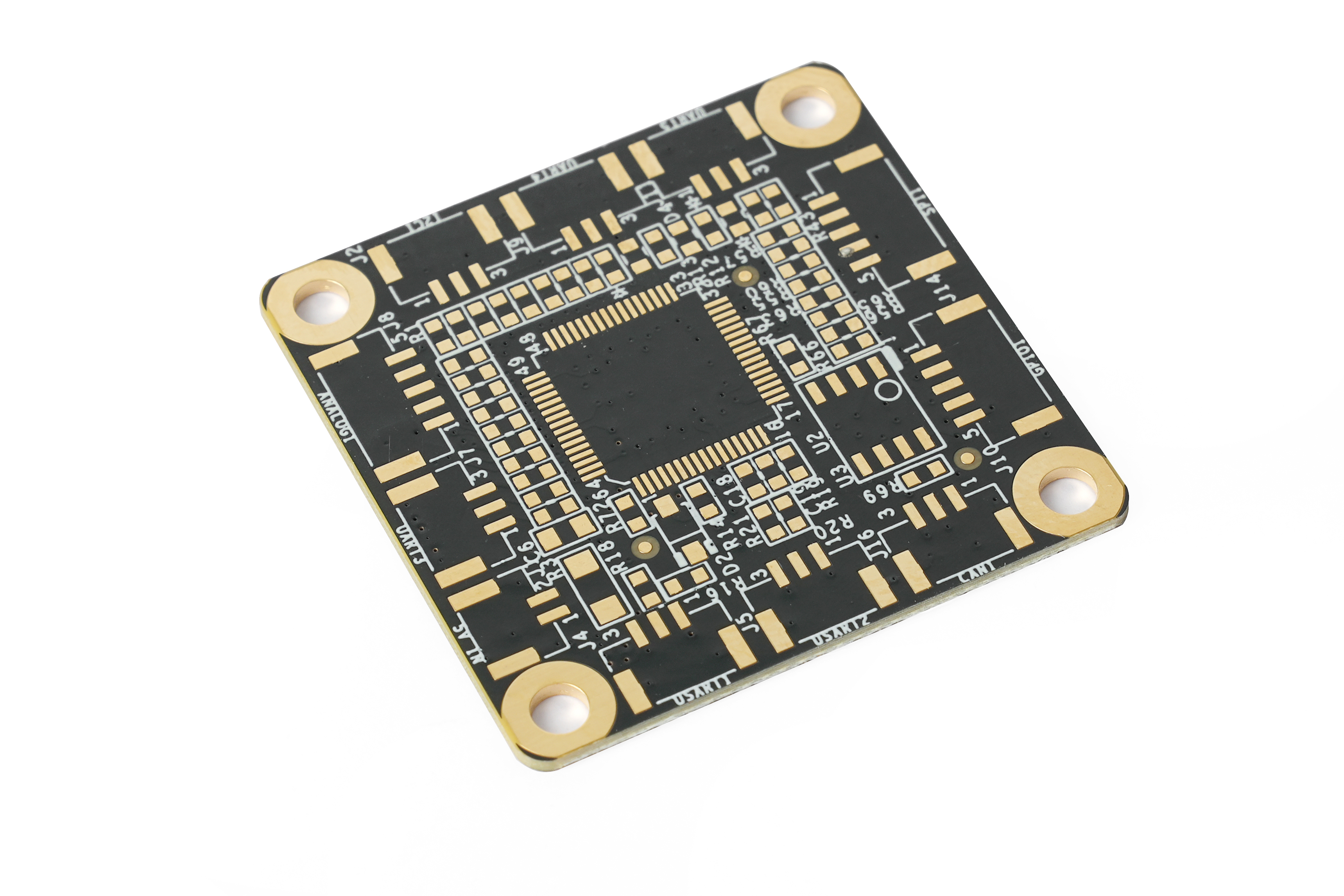
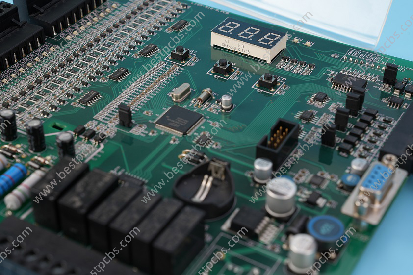
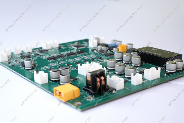
Normally, high power PCBs are featuring in thick copper thickness, wider trace space and distance, less or no BGA or fine pitch components. And because of the operation of high current, the circuit board is more likely to have the problem of heating, so the high-power PCB always do some heat treatment to avoid overheating, such as design dissipation via holes or adding some heat sinks. Anyway, effective power distribution is essential to ensure stable operation and prevent voltage drops in high power PCBs. Here we summarize some tips to optimize the power distribution when designing a high-power PCB.
High-Performance Materials
Choose materials suitable for high current applications like FR-4, metal substrates, or composite materials. These materials have lower resistance, higher thermal conductivity, and better mechanical strength to handle high currents and heat concentration.
Current Distribution Balance
Implement balanced current distribution by adding current balancers, balancing resistors, or current balance layers. This reduces the resistance and hot spots, enhancing reliability and stability.
Avoid Cross-Talk Between Power and Signal Traces
Keep high current paths separate from digital signal paths to minimize interference. This reduces electromagnetic interference (EMI) and improves overall performance.
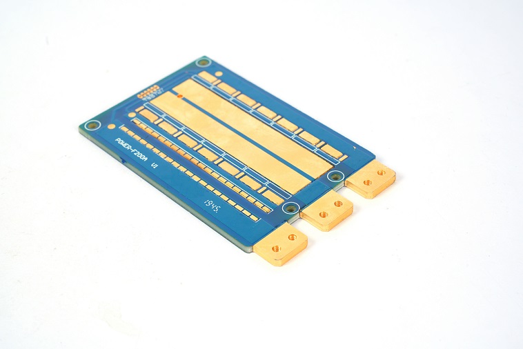
Solid Copper Pour for High Current Paths
Use solid copper pours for high current paths. This increases current-carrying capacity, improves heat dissipation, and minimizes voltage drops.
Thermal Management for Power Paths
Use large copper areas, vias, and exposed copper to enhance heat dissipation. Proper thermal management prevents component and product damage due to overheating.
EMC Radiation Control
Use wider trace widths, larger hole diameters, and increased spacing to manage EMC radiation. Keep high current paths short and place them away from sensitive components.
Why is Copper Thickness Critical in High Power PCB Design?
Copper thickness plays a vital role in determining the current-carrying capacity and thermal performance of high power PCBs. Here are some data points:
Standard Thickness: For high power applications, copper thickness typically ranges from 2 oz/ft² to 6 oz/ft².
Current Capacity: A 2 oz/ft² copper layer can handle approximately 10 amps, while a 6 oz/ft² layer can carry up to 30 amps.
Thermal Performance: Thicker copper layers improve heat dissipation, reducing the risk of overheating.
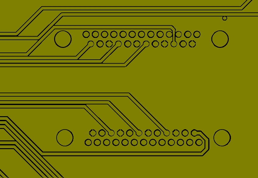
How Does PCB Layout Affect Signal Integrity in High Power Designs?
PCB layout is a critical factor that influences signal integrity and overall performance in high power designs. Consider these points:
Trace Length: Minimize the length of high-speed signal traces to reduce signal loss.
Consistent Trace Widths: Maintain consistent trace widths to ensure uniform current distribution.
Separation of Power and Ground Planes: Reduces noise and crosstalk.
Differential Pairs: Use differential pairs for high-speed signals to enhance signal integrity.
Adequate Spacing: Ensure adequate spacing between traces to prevent interference.
Designing a high power PCB requires a comprehensive understanding of various factors, including thermal management, material selection, power distribution, copper thickness, and PCB layout. By addressing these considerations, you can optimize your PCB designs for high power applications, ensuring reliability and performance. At EBest Circuit (Best Technology), we specialize in high power PCB solutions tailored to meet your specific needs. Our expertise and commitment to quality make us the ideal partner for your high power PCB projects. Choose EBest Circuit (Best Technology) for unparalleled performance and reliability in your PCB designs.