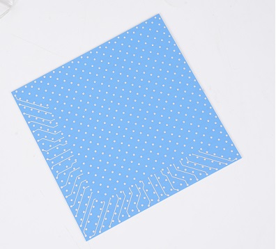
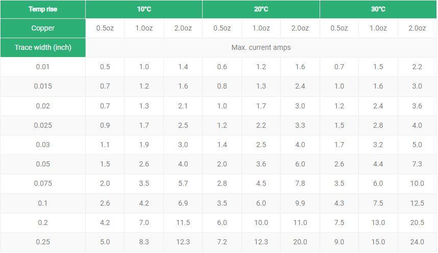
Trace width refers to the width of the conductive line on the PCB. If the line width is too narrow, the current passing through the unit area is too large, which will cause the wire temperature to rise and may damage the circuit board. Spacing refers to the distance between adjacent conductive lines on the PCB. Sufficient spacing can ensure the electrical insulation performance between adjacent lines and prevent short circuits between lines.
What is PCB trace/line spacing?
PCB trace/line spacing refers to the minimum distance between two lines on the PCB board. This distance is usually used to avoid electrical interference and ensure the reliability of the circuit. The size of the line spacing will affect the crosstalk, electromagnetic compatibility and heat dissipation performance of the circuit.
The basic concept and importance of line spacing is that it directly affects the performance and reliability of the circuit. The size of the line spacing needs to ensure that the electrical coupling and interference between the circuits are minimized to ensure the normal operation of the circuit.
What are the rules for PCB trace spacing?
The basic rule for PCB trace spacing is that the distance from the center of the line to the center of the line should be greater than or equal to 3 times the line width (3W rule) to ensure that crosstalk between lines is reduced.
- 3W rule: In order to minimize the interference between lines, the distance from the center of the line to the center of the line should be greater than or equal to 3 times the line width (3W rule), which can reduce 70% of the electric field interference. If you need to achieve a higher interference reduction effect, you can use 10 times the line width (10W rule), which can reduce 95% of the interference.
- Electrical safety spacing: According to the production capacity of the PCB manufacturer, the spacing between the wires and between the wires and the pads shall not be less than 4mil. Usually, the conventional spacing is set to about 10mil to ensure production quality and electrical safety.
- Special signal lines: For signal lines that need to control impedance, such as RF signals, important single-ended signals, and differential signals, the line width and line spacing should be determined according to the stacking calculation to ensure stable signal transmission.
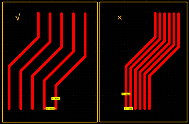
- Other considerations: In PCB design, it is also necessary to pay attention to the signal lines to avoid using right angles and sharp angles. Using arcs or 135° obtuse angles can reduce reflections and standing waves.
What is the minimum line spacing in PCB?
The minimum line spacing in PCB is usually 4mil. This spacing is to avoid electrical interference and ensure the reliability of the circuit. The specific line spacing requirements depend on factors such as design specifications, application environment, and manufacturing process.
In some high-precision applications, a smaller spacing may be required, but in general, the spacing should not be less than 4mil. The common spacing in conventional design is 10mil, which can ensure better production efficiency and circuit stability.
What is the minimum line width for a PCB?
The minimum line width of a PCB is usually 6mil (about 0.153mm). This is because in high-density and high-precision PCB design, the line width needs to reach this value to ensure production quality and reliability.
The minimum line width may vary under different design requirements. The minimum line width that can be supported may reach 3.5mil (about 0.09mm) or less, but in most common designs, the line width will be greater than this value to ensure production yield and reliability. In high-density and high-precision PCB design, the line width may be thinner.
When designing a PCB, the choice of line width needs to consider the needs of signal transmission. Generally speaking, the larger the line width, the better the factory production and the higher the yield. The line width in conventional design is usually 10mil (about 0.254mm), which can meet most application scenarios. In high-speed signal transmission, the line width needs to be greater than 10mil to reduce signal loss and synchronization problems.
What is the minimum hole spacing for PCB?
The minimum hole spacing of PCB is generally 0.1mm to 0.15mm. This range is applicable to standard 6-layer PCB circuit boards, but the specific value may vary depending on the manufacturing process and design requirements.
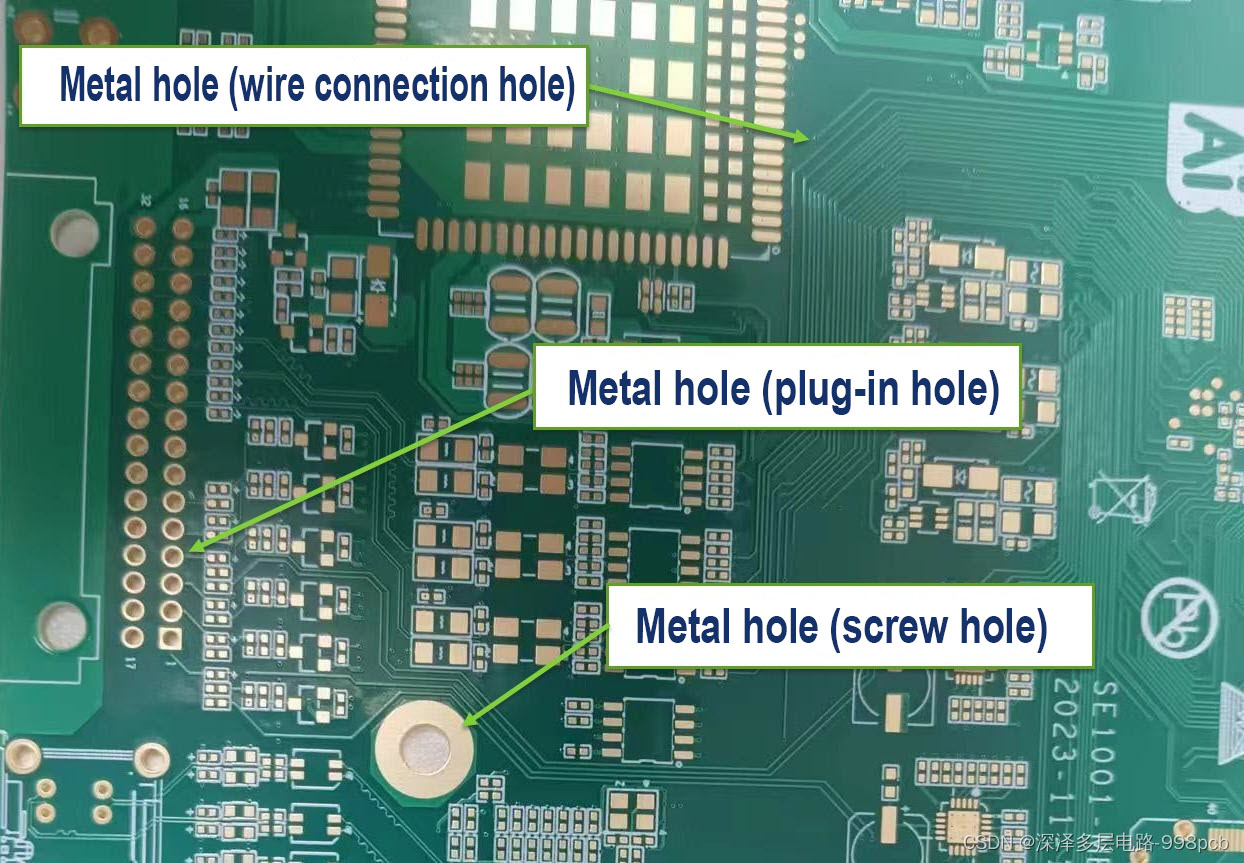
Under different manufacturing processes, the specific value of the minimum hole spacing is different. The minimum aperture of mechanical drilling is 0.15mm, while the minimum aperture of laser drilling can reach 0.075mm. In addition, the spacing from the pad to the outline is generally 0.2mm, and the single side of the pad cannot be less than 4mil (about 0.1mm), preferably greater than 6mil (about 0.15mm). For non-metallic holes and slots, the minimum spacing is not less than 1.6mm, and the slot hole is not less than 2.0mm from the edge of the board of the outline.
Factors that affect the minimum hole spacing of PCB include manufacturing process, design requirements and drilling detection. The advancement of manufacturing process has continuously improved the accuracy of PCB boards, and the minimum hole diameter and spacing have been continuously reduced. For example, the accuracy of modern PCB boards has developed to a minimum hole diameter of 0.08 mm and a minimum hole spacing of 0.1 mm or even higher. In addition, drilling detection is also an important link to ensure the quality of PCBs, including through holes, part holes, slot holes and special-shaped holes, which all need to be strictly inspected.
Why is PCB trace spacing design so important?
PCB trace spacing design is very important because it is directly related to the reliability, performance and safety of the circuit board. By reasonably designing the trace spacing, electrical interference can be avoided, signal transmission quality can be guaranteed, and the thermal stability and reliability of the circuit board can be improved, thereby ensuring the normal operation and long-term stable operation of the circuit board.
First, the design of trace spacing can prevent electrical interference. When two traces are parallel and close to each other, parasitic capacitance and inductance will be generated between them, resulting in signal interference and attenuation. Increasing the trace spacing can reduce this coupling effect, thereby ensuring stable signal transmission.
Second, appropriate trace spacing helps to improve the thermal stability of the circuit board. Components and traces with large working current will generate heat when working. If the traces are too dense, heat is easy to accumulate, resulting in local temperature rise, which may cause failure.
In addition, the design of trace spacing also needs to consider the requirements of production process. Smaller line width and line spacing have higher requirements for production process, which may increase production difficulty and cost.
What will happen if the PCB trace spacing is insufficient?
Insufficient PCB trace spacing will lead to problems such as signal attenuation, signal delay, crosstalk interference and layout difficulties. These problems will affect the performance and stability of the circuit and may even cause circuit function failure.
First, signal attenuation is a major problem of insufficient spacing. Signals will be attenuated during transmission. Too small spacing will increase the possibility of signal attenuation, resulting in signal distortion and increased noise, especially in high-frequency signals and fast signal transmission.
Second, signal delay is also a problem caused by insufficient spacing. It takes time for signals to propagate in the circuit. Too small spacing will extend the path of signal propagation, thereby increasing signal delay and affecting the real-time performance of the system.
In addition, crosstalk interference is another important issue. Insufficient spacing will increase the electromagnetic interaction between signal lines, leading to crosstalk interference, thereby introducing errors or interference and affecting the stability of the circuit.
Finally, layout difficulties are also a practical problem caused by insufficient spacing. When laying out the PCB, too small spacing will increase the complexity of the layout, making it difficult for designers to reasonably arrange the signal path, the distribution of power and ground lines, and the layout of components.
Does trace spacing affect PCB production cost?
The setting of trace spacing is directly related to the difficulty and cost of PCB production process. Although smaller line width and spacing can improve the performance of the circuit, it will increase the difficulty and cost of production.
The setting principles of trace spacing include:
The default values of line width and spacing are usually 6mil, but they can be adjusted according to design requirements. The minimum line width recommended value is 10mil, and the maximum line width can be set to 200mil.
The setting of trace spacing needs to take into account electrical safety and signal integrity. It is usually required that the line center spacing is not less than 3 times the line width to ensure that the electric field does not interfere with each other.
In the design of high-speed signal lines, using larger spacing can further reduce crosstalk and improve the stability of the circuit, but it will also increase costs.
Factors that affect the cost of PCB production also include:
- Number of wiring layers: The more layers, the higher the price.
- Via size: Vias smaller than 0.25mm usually require additional fees, and back drilling will increase the cost by about 10%~20%.
- Plate selection: Unconventional materials such as high-frequency plates and halogen-free plates will increase procurement cycles and production costs.
In summary, the setting of trace spacing has a significant impact on the cost of PCB production. Reasonable settings can control costs while ensuring performance.
In short, PCB line width and spacing are very important parameters in electronic circuit design. They directly affect the performance, reliability and manufacturing feasibility of the circuit board. When designing a circuit board, it is necessary to reasonably select line width and spacing according to the requirements of the circuit and the actual situation.