Global demand for supplies used by our customers to treat and help protect people, such as respirators, is currently exceeding supply. EBest Circuit (Best Technology) expects demand for respirators to outpace supply for the foreseeable future.
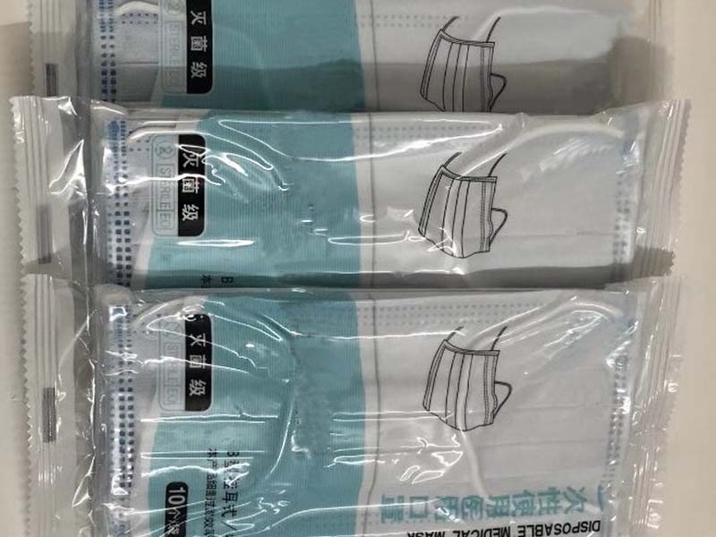
disposable face mask
Throughout all the recent developments, EBest Circuit (Best Technology) is working hard to uphold the commitments we made to supporting your business. We are very focused on protecting the health and safety of our workforce while maintaining the ability to keep serving you.
With more than 10 years of domain expertise in the industries we serve, we are here to help you adjust to whatever may happen next.
The COVID-19 pandemic continues to affect all of us, and all EBest Circuit (Best Technology) colleagues are working around-the-clock to help provide critical tools for the fight. Our current focus: supporting health care and front-line workers as well as our regular and new customers around the world by providing products they need to help protect their lives.
We are seriously in choosing partners who can provide various kinds of respirators as well as medical products:
The partners who can double their global output rate to nearly 100 million respirators per month are in our priority;
Also, we anticipate doubling global capacity of our partners to almost 2 billion respirators in the next 12 months.
We have not increased the prices we charge for our respirators in this crisis.
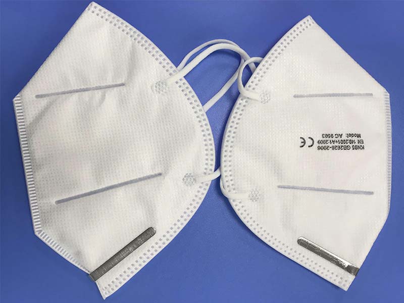
KN95 face mask
Our efforts are guided by our value of Caring – for our people and their families, our consumers, and importantly, for those most in need right now. We want to share a few of the ways that we are responding to this global health crisis.
Moreover, after our efforts, all of our face masks, KN95 masks and all of other medical products have passed GB2626-2006 and CE standard. You can also find out the certificates from the above website.
Anything I can do for you? If there is a need, contact us anytime. Our sales team will be here to reply you instantly. Please keep safe and take good care of yourself and your families. Come on, our friends, wish the pandemic will end asap and everything can return to normal soon.
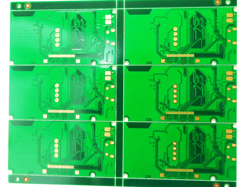
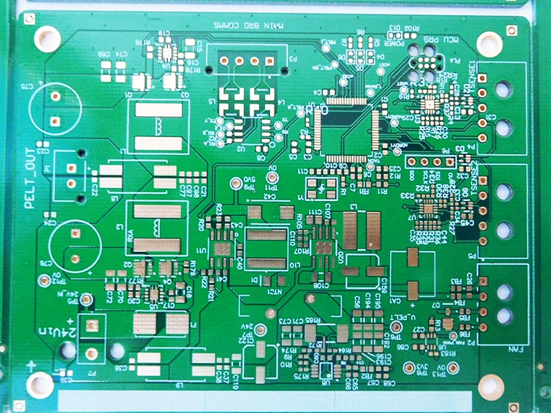
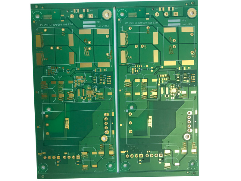
PCB is an indispensable part for any electronic equipment in small toys or computers., etc. The complex interconnection components include resistor, diode and capacitor, which help components work normally in series. In a sense, it is similar to the “brainâ€Â of the system. PCB assembly process must be of no any mistakes. Here are some points that need to be paid attention:
1.Supply chain management: In order to create high quality PCB, the first thing needing consideration is supply chain. For the availability, both quality and price are important, so is delivery time of components.
pcbassembly
2.PCB layout. The common question during manufacturing stage is pcb layout in minor differences. Even though various types of designs looks the same to outward seeming, the manufacturing processes are different. You need to ensure PCB layout is feasible during manufacturing process.
3.Test-test has to be conducted after PCB assembly. What needs to be done is to design test point. Some tests include:
Micro-section analysis-also referred to as cross section analysis. This test contributes to identifying components fault and thermal-mechanical faults.
pcbassembly
Solderability test. This test contributes to testing reliability of PCB solder pad, to ensure a firm surface and a reliable soldering point. It also contributes to confirming if storage will have an effect on solder components.
PCB pollution test-This can test many issues, such as corrosion and degradation. Scaling powder residue will result in pollution and thereby case components failure. Pollution analysis is famous for its accuracy and preciseness.
Optical microscope-This can test the issues relevant to PCB and soldering as well as overall pcb assembly. The process is famous for its speed, as it involves using high-power microscope to inspect incorrect structure.
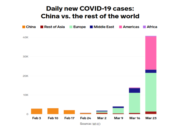
China’s fight against COVID-19 epidemic has achieved victory at this stage. Infected patients were found in 337 cities in China but now only 28 cities remaining patients in cure. So far till March 31st, there were 82545 confirmed cases in China, while 76225 cured and only 3006 remaining now. Most importantly, many of the areas finds only one figure number increase and others stop increasing for quite some days. If the first half of COVID-19 fighting is inside China national territory, the second half will be on the international stages while noticeable growth on COVID-19 infected cases are spreading all over the world now.
corona virus updates
EBest Circuit (Best Technology) has been collecting the measures in China on epidemic controls so in order to provide a more objective and useful reference for overseas professionals which we hope they could refer to and protect better themselves from the COVID-19.
Governmental Measures
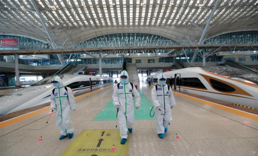
During the height of the outbreak, trains didn’t stop at the disease’s epicenter, Wuhan
Wuhan trains
Trains, as well as other tightly packed forms of transportation, can serve as vectors of illness. The more people, the more closely packed, and the more poorly ventilated the space, you can imagine that’s a bad situation because there are a ton of people, they’re in very close quarters, and they’re a totally captive audience. Cutting off transportation was considered on the top three measures to contain the spread of the virus.
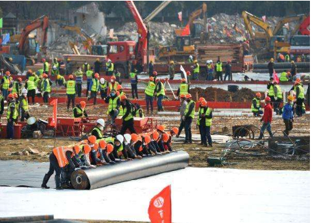
China built new hospitals in a rush, with workers toiling night and day to get them done.
China Newly-built Hospitals
China built two new 1,000-1,300-bed hospitals to fight the corona virus, one created in six days, and the second in 15 days, using prefabricated modules.
Corona virus testing was easily accessible and free
Corona virus testing
In China, patients who were confirmed to have the corona virus were either sent to an isolation center or hospital. The government also made clear that testing for the new virus was free, and COVID-19-related charges that weren’t covered by a person’s insurance would be paid for by the government.
The country implemented large-scale contact tracing in the early 2000s
Contact tracing
During the SARS outbreak in 2002-2003, China set up large-scale surveillance systems that included contact tracing, a front-line public-health strategy that involves identifying and following up with people who may have come into contact with an infected person.
The country postponed non-urgent medical care and moved many doctor’s visits online. Not all patients were given the critical care they needed during the outbreak, though
Doctor’s online visit
In China, elective surgeries and other non-critical doctors’ visits were delayed, and many medical services were moved online. Someone in one place said 50% of their consultations are now done online; they just moved a whole bunch of what was normally done physically online to be able to keep the regular health services going.
Centers for Disease Control exploring a way of therapeutic plan combing Traditional Chinese medicines and Western medicines.
Traditional Chinese medicines treatment
The combination of Traditional Chinese medicines and Western medicines had been proven effective on the SARS fights. Doctors of traditional Chinese medicines had volunteered for consulting and participating into the virus fights.
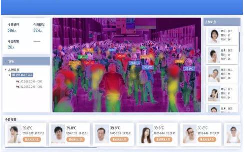
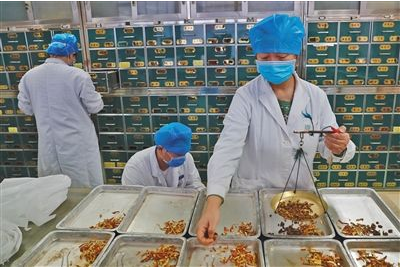
China used technology that aims to trace every single COVID-19 case
Civilian Measures
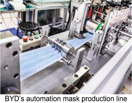
Traditional epidemic prevention manufacturers speed up and similar production lines integrating to make more necessary products
mask production line
Many medicinal and pharmaceutical substances manufacturers launched automation assemble lines and increase manpower to speed up the mass production of necessary drugs, masks, ventilators to meet the huge consumption during virus fighting. Many of these companies arranged 24-hour shifts for maximizing the production.
Meanwhile other manufactures such as automotive OEM had change their assemble line into masks productions machines.
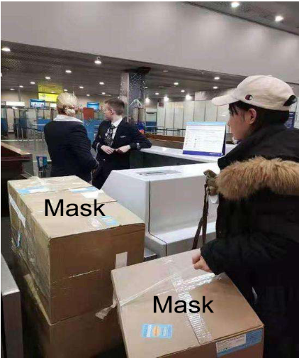
At the blast of COVID-19, returning Chinese carrying back epidemic products from overseas as much as they can
epidemic products brought by overseas Chinese
Returning travelers carried extra masks on their flights back to China and donated them to the hospital and governments in need. Some overseas Chinese unions also had helped ordering these products and sending to China.
Chinese citizens did their part to curb the disease’s trajectory on an individual level, too, though we may never know the true scale of their complaints or sacrifices in this outbreak.
China’s road
In contrast to reports in the US of people clamoring over the last hand-sanitizer, the attitude of people in China was that they were all in this together. People stay at home for self-quarantine, lockdown and response to the postpone returning to work and school.
People who thought they might have the corona virus could go to one of the nation’s many fever clinics
fever clinics
People who thought they had the novel corona virus in China would often be sent to a special fever clinic, which have been widespread since the country dealt with an aggressive SARS outbreak in 2002. Their temperature would be taken, and they’d discuss their symptoms, medical history, travel history, and any prior contact with anyone infected with a doctor.
If necessary, patients might receive a CT scan, which is one way to do an initial screening for COVID-19. Each machine did maybe 200 a day. 5-10 minutes/scan. A typical hospital in the West does one or two an hour.
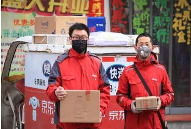
People quickly shifted jobs in order to assist during the outbreak
volunteers
When it came to the non-medical response, there was a nationwide sense of solidarity with Hubei. Other provinces sent 40,000 medical workers to the center of the outbreak, many of whom were volunteers.
Workers in transportation, agriculture, and clerical positions were encouraged to new positions such as delivery, courier and epidemic prevention manufacturing, too.
While staying home, it’s been relatively easy for Chinese people to get extra food and supplies
Enough food
China essentially mandated a country-wide shut down, demanding that every Chinese resident stay home until the curve was flattened. But in West, unlike China, a country-wide shutdown would be difficult to enforce.
Fifteen million people had to order food online. It was delivered. Yes, there were some screw-ups. But few said: every now and again there’s something missing from a package, but food supply is pretty much normal via ordering online.
If you’ve ever made a pie with your kids, you know that the thickness of your crust is important. Too thin, and the pie falls apart into a mess of filling. Too thick, and you might as well be chewing on a loaf of bread. Getting the thickness just right is what makes a pie worth eating.
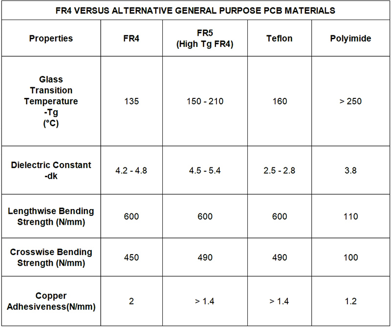
Even though PCB substrate materials are non-conductive and do not carry current, the board material still affects the electrical performance. FR4 PCB substrate is widely used, and a thorough understanding of this material is very necessary.
FR4 PCB
FR4 Thickness Design Considerations
If you start your design process by choosing the correct board thickness, you will avoid to redesign later. A number of factors are influenced by the board thickness. Before you start designing your board, think about the following design issues:
Form factor and flexibility: Does your PCB have a strict form factor requirement? Thinner boards tend to be used in smaller devices and can flex more than a thicker board. A more flexible board may be unusable with a pick & place machine. Electrical connections in flexible boards can also break unless they have some mechanical support.
Components and connections: Will the device have any components that require the Printed Circuit Board to have a specific thickness? Components like USB edge connectors and some through-hole components require PCB in correct thickness. BGA connectors generally require thicker boards.
FR4 PCB
Impedance matching: Traces on adjacent layers in multi-layer boards form a capacitor, and the layer thickness and its dielectric constant determines the equivalent capacitance. Impedance matching is critical, and the capacitance must be taken into consideration when designing the board. This is especially true in HDI PCB.
High-speed devices: If you are working with a high-speed device, FR4 is always not the best option, and some other material should be used instead. FR4 PCB could be used in high-speed devices when the layers are coated with high-speed laminates. These laminates offer significantly improved electrical performance over standard FR4, and generally a combination of FR4 and a high-speed laminate may be preferable to an alternative material.
RF losses: FR4 tends to have higher losses than other PCB materials that are specialized for RF applications. Traces on FR4 will have larger attenuation at RF frequencies than other specialized materials for a given board thickness. The board thickness also changes the effective dielectric constant of the board, which then changes the required impedance matching in RF circuits.
Thermal and Reliability Considerations
All materials expand at higher temperatures, and the thermal expansion coefficient must be taken into consideration when choosing the board thickness. The thermal expansion coefficient of FR4 changes drastically above the material’s glass transition temperature (140℃). The board can become electrically and mechanically unstable when the board operates above the glass transition temperature.
The reliability of the trace materials, laminate materials, and solder joints on a PCB laminate are determined by the resistance to thermal cycling. When the thermal expansion coefficients of the different materials are mismatched, fatigue occurs after repeated thermal cycling. Copper plating in vias and solder balls are especially vulnerable to damage under thermal cycling.
This is a greater problem in thick FR4 PCB with high aspect ratio vias. Plating damage in through-hole vias, lifted pads, and cracked surface resin can occur under the stress caused by thermal cycling. A thicker board will have a larger expansion magnitude for a given via aspect ratio, resulting in more damage to the board and the electronic components. Thermal stresses can be huge when an FR4 PCB runs above the glass transition temperature.
Volumetric expansion is also critical in rigid-flex FR4 PCB. Thermoplastic adhesives with low glass transition temperatures and high Z-direction expansion coefficients can exhibit very large volume expansion at high temperature. Z-direction expansion in these situations can be as large as 500 ppm/ƒ.
Even though a thicker FR4 PCB has greater thermal mass and can dissipate more heat from electronic components, there is also the potential for more damage due to thermal expansion. Therefore, how to choose between a thick and thin FR4 PCB that satisfies all other requirements, the thinner board may be a better choice if the FR4 PCB will undergo thermal cycling frequently.
If you have any comments. queries or suggestions on this, welcome to contact us.
As a general rule, this thickness of copper foil for single-sided PCB and double-sided PCB is approx.35um(1.4mil). There is also another specification, which is 50um and 70um. The surface thickness of multilayers PCB is 35um(1oz(1.4mil)) generally, and the inner layer has a thickness of 17.5um(0.7mil). 70% of PCB uses the copper foil thickness of 35um. This is based on PCB purpose and signal voltage as well as current. In addition, for PCB requiring large current, copper thickness of 70um or 105um will be used, and 140um is also used in some cases.
heavy copper pcb
People often use OZ to represent copper thickness. 1OZ stands for the thickness of 1OZ copper covered on the area of 1 square feet evenly. I.e. approx. 1.4mil. The weight of unit area is used for representing the average thickness of copper foil. I.e. 1oz=28.35g/ FT2(FT2 stands for square feet, 1 square feet=0.09290304 square meter).
For heavy copper PCB, if the substrate has a thickness of 1 to 3mm, then the thickness of composite copper foil will be approx.35um. If the substrate has a thickness of less than 1mm, then the thickness of composite copper foil will be 18um. If the substrate has a thickness of above 5mm, then the thickness of composite copper foil will be 55um.
heavy copper pcb
The thickness of copper foil(wiring width) will influence current. Even though there is a formula to directly calculate the largest current loading capability of copper foil, things will get more complex when designing wiring. In this case, safety should be fully taken into consideration during design.
Copper foil will have different thickness, if there are different purposes. General 0.5OZ, 1OZ and 2OZ copper foil are most widely used for consumption and communication products. The thickness of copper foil above 3OZ belongs to heavy copper products, which are widely used for products with large current, such as high pressure products, and power supply board.
This is all about how to choose proper copper thickness during your project. Hope this is helpful to you. If you are still confused, please contact EBest Circuit (Best Technology). We have online customer services for 24 hours.
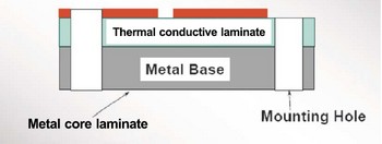
With the development of LED technology, LED power keeps increasing. This is closely related to heat dissipation. In order to resolve heat dissipation of LED with big power, aluminum-based copper-clad laminate is highly applied in led strip field.
Aluminum PCB(metal-based heat dissipation board) is a kind of unique metal-based copper-clad laminate. It has good head conductivity, electrical insulation and machining performance. Single-sided aluminum pcb consists of three layers of structures:circuit layer(copper foil), insulation layer and metal-based layer. Circuit layer requires large current-carrying capability, so we should use thick copper foil(generally 35um to 280um). The insulation layer for heat conduction is the core technology of aluminum pcb. It is general composed of special polymer filled with special ceramic. Small heat resistance, excellent viscoelasticity and anti-aging are all its advantages. And it is also able to bear mechanical and heat stress. Metal-based layer is the supporting component of aluminum pcb, and it needs to have high heat conductivity, so we generally use aluminum board, or copper board(which can provide higher conductivity). And it is suitable for regular machining such as drilling, punching and cutting. Techniques include gold plating, solder levelling, osp, ENIG, lead-free ROHS and so on.
single-layer-mcpcb-stackup
Aluminum pcb is commonly seen in LED products and has two sides(the front side and the reverse side). The white face is used to solder LED pin, and the other face presents natural color. It is generally painted with thermal conductivity paste and then contacted with heat conduction part. LED aluminum pcb is mainly used in power amplified mixed integrated circuits for STK series, motor cycles, automobile and electronics field.
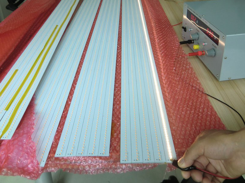
There are many kinds of aluminum pcb for led tube, which varies based on the length and width of led tube. Aluminum pcb for led tube is popular with people due to its good quality, and durable and energy-saving features.
led strip
Aluminum pcb for led tube can save electricity as high as 70%. The light intensity of 12W Led tube is equal to 40w fluorescent tube. The service life of LED tube is is more than 10 times that of general fluorescent tube. It can be free of maintenance. Also, there is no need to change LED tube, barratter and starter frequently.
Generally, fluorescent tube has high temperature inside and needs to be used for more than 10 hours everyday in most cases. This problems are perfectly resolved by aluminum pcb for led tube.
If you have any queries, comments or suggestions on aluminum pcb for led, welcome to leave your message.
Confirm the processing method of the hole: Drilling and punching are used to process the holes of mcpcb multilayer. The feed degree and rotating speed of drilling is different from FR-4 PCB material. Adjustment needs to be made according to base material. Generally, we set the feed degree at 1-1.5 mil/rev, and the rotating speed at 20000-60000RPM. Punching requires specialized tooling to meet the needs of metal punching.
Outer Layer Drilling-the 2nd production process of mcpcb multilayer
Drilling of the inner layer core board should be carried out, according to the drilling parameters of FR-4 PCB. There should be enough vacuum degree and pressure foot, for keeping holes clean and removing debris. The number of drilling holes and wear condition should be well controlled.
Making Inner Layers-the 3rd production process of mcpcb multilayer
During the process, we use dry film(1.3-2.5 mil water solubility light induced corrosion resistant dry film), and wet film(wet film light induced corrosion resistant solvent).
Circuits Electro-Plating/Etching-the 4th production process of mcpcb multilayer
Circuits Electro-Plating: Acid copper plating and tin plating are suitable for double-sided core board.
Etching: During etching process, we need to adjust speed according to the thickness of copper foil. In order that core board can be etched smoothly, we can reduce pressure of etching spraying, or make towing plate.
After lamination, when epoxy resin is completely cured, and epoxy resin of board is removed, 2nd drilling should be carried out. This operation involves mechanical processing of metal-base composite material. This is a challenge to structure of mcpcb multillayer. Special attention should be paid during operation, especially location precision and quality of processing holes.
Making Soldermask-the 7th production process of mcpcb multilayer
There are 4 ways for making soldermask: liquid light induced corrosion resistant solvent; Thermosetting soldermaskï¼›UV curing soldermask; Dry film soldermask.
Surface Finishing-the 8th production process of mcpcb multilayer
In order to facilitate assembly of components, exposed copper foil surface must be treated, for enough solderability, good bonding power and comprehensive manufacturing performance. There are 4 ways for surface finishing: HASL, OSP, Sn and Ni/Au.
Packaging of mcpcb multilayer is important for reducing abrasion mark and wear. Using low-sulfur sheet for vacuum sealing is a good choice. Foam can also be used separately. The key is to isolate soldering flux from aluminum surface, in this way, we can eliminate galvanic electricity reaction between different metals.
The primary advantage of ceramic multilayer PCBs lies in their thermal properties. The most significant of these is thermal conductivity, which outperforms traditional materials by a tremendous margin. In the table below, the most used board material, FR4, is compared with the ceramic multilayer board in a number of important categories.
ceramic pcb
MULTILAYER PCB MATERIAL COMPARISON
Ceramic
Versus
FR4
28 – 280
Thermal Conductivity (Wm-K)
0.8 – 1.1
Component Comparable
Coefficient of Thermal Expansion (CTE)
Component Comparable
High
Frequency Performance
Low – Mid
Fragile
Handling
Easy
Low
Availability
High
Mid – High
Cost
Low – Mid
As shown above, ceramic multilayer PCBs have advantages and disadvantages as compared to FR4. However, the advantages point to a continued increase in the use of ceramic boards for high-speed and high-power applications that are criteria for more functionality in smaller packages.
ceramic pcb
EBest Circuit (Best Technology), the industry leader in fast, precision and high-quality PCB manufacturing, has a wide range of material options including to meet your design objectives. This includes accommodating the special process of using ceramic materials for your board if desired. We also strive to provide you with the best manufacturing experience.
HDI PCB (High Density Interconnector PCB), is a printed circuit board having a relatively high line distribution density using the micro-blind and buried hole technology.
It is a process that includes an inner layer line and an outer layer line, then uses a hole and a metallization in the hole to realize a joint function between the inner layers of each layer.
HDI PCB-1
With the development of high-density, high-precision electronic products, the requirements of high-density and high precision are imposed on printed circuit boards. The most effective way to increase the density of pcb is to reduce the number of through holes, and to accurately set the blind holes and buried holes to achieve this requirement, thereby an HDI PCB came into being.
HDI PCBs are finding their way into a growing number of products:
Military communications devices and other strategic equipment
Aerospace – smaller space requirements and light weight are ideal for such applications
Computers and smartphones – phones and computers are taking full advantage of smaller profiles, reduced weight, and increased functionality, made possible through the integration of HDI circuits.
HDI PCB-2
Medical equipment – diagnostic and monitoring equipment has become more reliable and expanded with technical features that aid medical teams with patient treatment, and all of this is powered by HDI PCBs and advanced software.
HDI PCB utilizes buried or blind vias, or a combination, and may also incorporate microvias with an incredibly small diameter. This facilitates the incorporation of more technology in less space, with fewer layers. Multi-layer HDI PCB are also in common use, with many layers being accommodated through various construction methods utilizing blind, buried, stacked, and staggered vias.
With smaller components and blind via in pad technology, components may be placed closer together, resulting in faster signal transmission rates while also reducing crossing delays and signal loss. These are key considerations that generate improved performance of HDI PCBs.
HDI PCBs are preferred for applications where space, performance, reliability, and weight are concerns. This makes them more suitable for nearly every application related to electronics, consumer products, computers, and aeronautics.
Multi-layer HDI PCB can provide strong interconnection of stacked vias, resulting in high levels of reliability, even in more extreme environments.
Considering this, do you ever think about choosing HDI PCB on your next project?
FR4 is the most common material grade that comprises fabricated PCB. FR indicates the material is flame retardant and the 4 indicates woven glass reinforced epoxy resin. Single or double-sided PCB structures consist of an FR4 core and top and bottom copper layers. Multi-layer boards have additional prepreg layers between the center core and top and bottom copper layers. Now, the core consists of a substrate with copper covering, also referred to as a copper clad laminate. The core, laminate, and prepreg may all be FR4 with the copper sheets between the signal and ground layers.
FR4 PCB
The properties of FR4 may vary slightly depending on the manufacturer; however, it generally has favorable strength and water resistance attributes that support its widespread usage as an insulator for many electrical applications. It serves the same purpose in PCBs, namely to isolate adjacent copper planes and provide overall bending and flexural strength for the structure. FR4 is a good general purpose material for PCB fabrication; however, alternative materials are available.
Alternative PCB Materials
Prior to the explosion of multilayer FR4 PCBs, there were many alternative board materials to FR4. These included FR2, CEM 1, and CEM 3, which were paper-based. However, the strength of FR4, especially for multilayer boards, was a major factor in separating it from alternatives to become the industry standard. Today, there are other materials that are used for single-sided, double-sided, non-plated through-hole (NPTH), and multilayer PCBs, in addition to FR4. These are compared in the table below:
FR4 Material VS Other Materials
The results above clearly indicate that FR4 is a good general purpose material as its parameters are mostly comparable to the other alternatives. It excels in structural integrity with a 2.0 N/mm copper adhesiveness and matches the alternatives in bending strength.
FR4 PCB
FR4 is the most widely-used material in PCB construction. Boards made from FR4 are strong, water resistant, and provide good insulation between copper layers that minimizes interference and supports good signal integrity. At EBest Circuit (Best Technology), the industry leader in fast, high-quality PCB prototype and PCB manufacturing, we are capable to meet your board material needs for any case. We will work with you to help you select the materials that will best implement your design intent.
Should you have any queries about FR4 material, contact us anytime, and our sales representative will give you a response at our soonest convenience.