Why Choose EBest for Your COB High-Power LED Module Copper Core PCB?
When you need a COB High-Power LED Module Copper Core PCB – High Thermal Conductivity for Brightness Stability, EBest is your first and best choice. Our products deliver unmatched performance to ensure your high-power LED modules operate reliably and stably.
Core parameters of our COB High-Power LED Module Copper Core PCB: Thermal conductivity up to 400 W/m·K, copper core thickness ranging from 0.8mm to 3.0mm, operating temperature range of -40°C to +125°C, dielectric layer thickness of 0.1mm to 0.3mm, and brightness stability deviation of ≤2% over 10,000 hours.
For consistent performance, reliable supply, and professional support, order your COB High-Power LED Module Copper Core PCB from EBest today—we provide the high-quality products your projects demand.
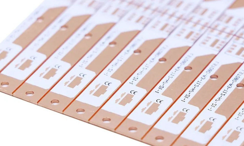
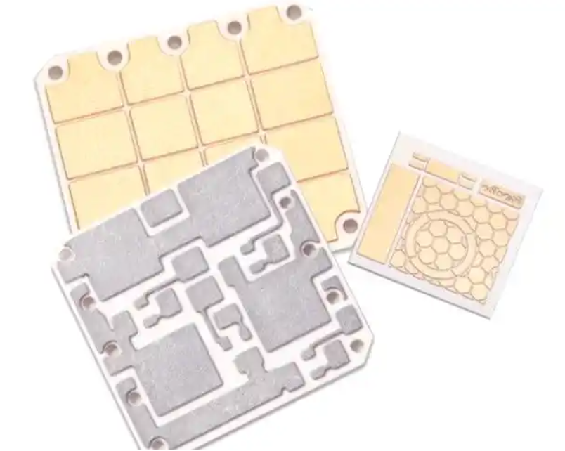
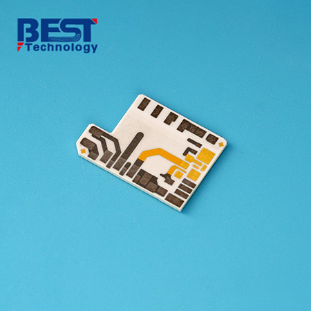
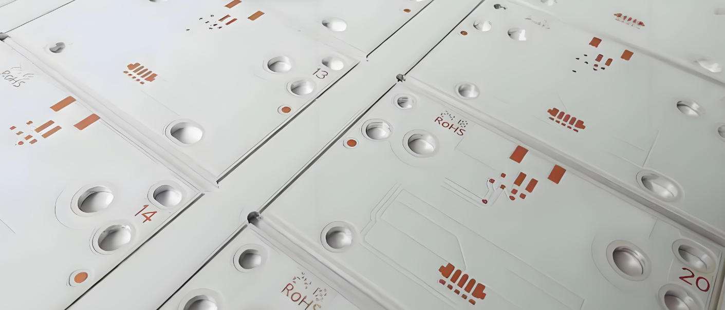
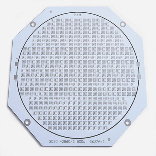
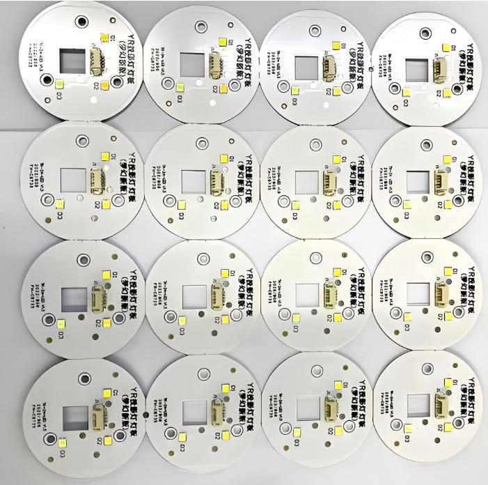
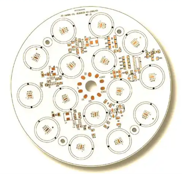
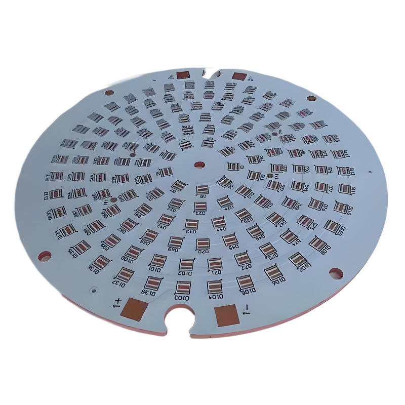
Copper Core PCB

Why Choose Us for COB High-Power LED Module Copper Core PCB?
Quality Assurance: Our COB High-Power LED Module Copper Core PCB undergoes strict multi-step testing (thermal shock, continuity, and insulation) to ensure its thermal conductivity and brightness stability meet global standards.
Lead Time Guarantee: We have a mature production line to ensure on-time delivery—standard orders ship within 7 to 10 days, and urgent orders can be fulfilled in 3 to 5 days without compromising quality.
Cost-Effectiveness: Through optimized supply chains and large-scale production, we reduce unnecessary costs, offering you high-quality COB High-Power LED Module Copper Core PCB at competitive prices.
Professional Service: Our technical team provides 24/7 support—from design consultation to after-sales troubleshooting, we assist you in resolving all issues related to your COB High-Power LED Module Copper Core PCB throughout the process.
Supply Chain Stability: We source high-purity copper and premium dielectric materials from trusted global suppliers, ensuring stable supply and consistent product quality for every batch.
What Are the Common Pain Points with COB High-Power LED Module Copper Core PCB, and How Does EBest Solve Them?
Many users encounter various performance-related issues when using COB High-Power LED Module Copper Core PCB—we address these pain points directly with proven solutions.
Pain Point 1: Poor thermal conductivity leading to module overheating and reduced brightness stability. Solution: We use high-purity copper cores and optimized dielectric layers to ensure a thermal conductivity of up to 400 W/m·K, effectively cooling LED modules and maintaining stable brightness.
Pain Point 2: Inconsistent product quality across batches. Solution: We conduct 100% full inspection on each COB High-Power LED Module Copper Core PCB to ensure every unit meets the same high standards.
Pain Point 3: Delayed deliveries disrupting production schedules. Solution: Through streamlined production processes and scientific inventory management, we ensure on-time delivery, even for large or urgent orders.
Pain Point 4: Lack of technical support for design and application. Solution: Our expert team offers free design consultations to help you optimize the design of your COB High-Power LED Module Copper Core PCB for your specific application scenario.
For hassle-free, high-performance COB High-Power LED Module Copper Core PCB, choose EBest—we turn your pain points into peace of mind.
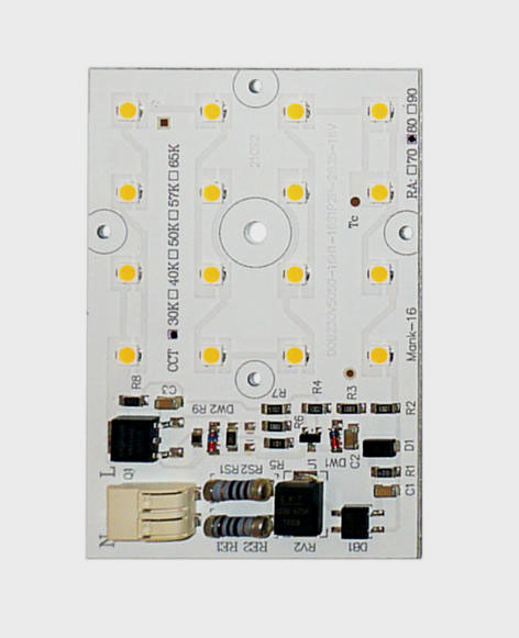
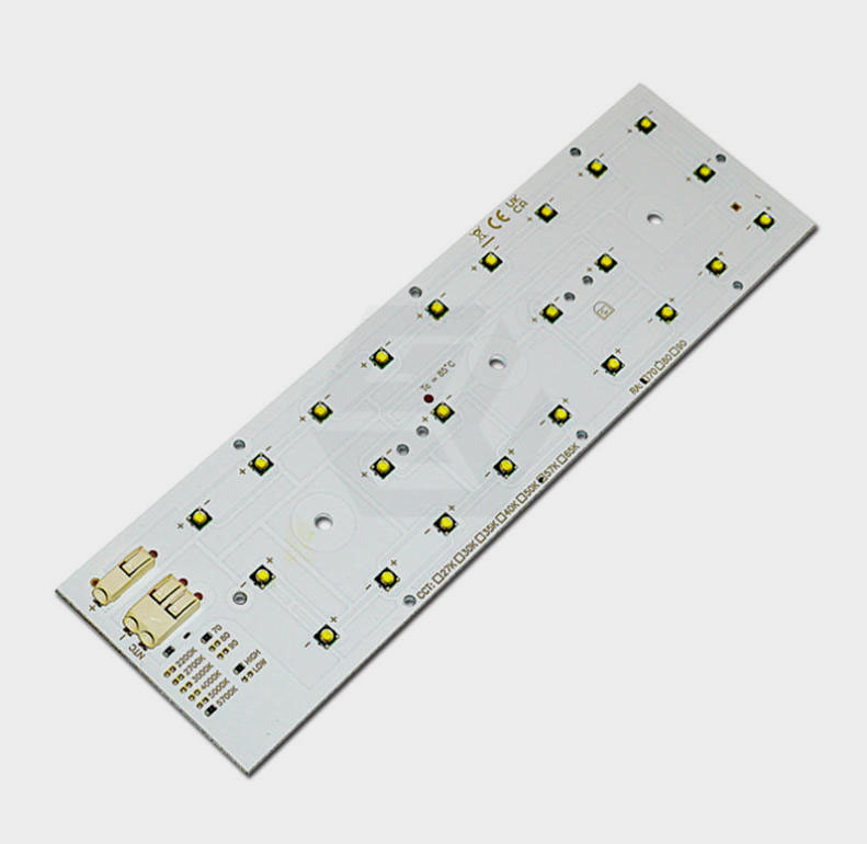
What Is a COB High-Power LED Module Copper Core PCB, and Why Is It Critical for Brightness Stability?
A COB High-Power LED Module Copper Core PCB is a specialized circuit board with a copper core, designed specifically for mounting COB (Chip-on-Board) high-power LED modules. Its core function is efficient heat dissipation, which directly affects the brightness stability of LED modules.
High-power LED modules generate significant heat during operation. Without timely heat dissipation, LED chips will overheat, leading to dimming, color temperature shift, and shortened service life.
The copper core in our COB High-Power LED Module Copper Core PCB has excellent thermal conductivity, which quickly transfers heat generated by LED chips away, maintaining stable chip temperature and thus ensuring consistent brightness and long-term reliability.
How Does High Thermal Conductivity in COB High-Power LED Module Copper Core PCB Improve Brightness Stability?
High thermal conductivity in COB High-Power LED Module Copper Core PCB directly improves brightness stability by preventing LED chip overheating—the primary cause of brightness degradation in high-power LED modules.
When LED chips overheat, their light output decreases (known as “light decay”), and color temperature shifts, resulting in uneven brightness across the module.
Our COB High-Power LED Module Copper Core PCB has a thermal conductivity of up to 400 W/m·K, dissipating heat much faster than standard PCBs. This maintains a stable chip temperature, eliminates light decay, and ensures consistent brightness throughout the module’s service life.
What Key Specifications Should You Look for When Selecting a COB High-Power LED Module Copper Core PCB?
When selecting a COB High-Power LED Module Copper Core PCB, focus on the following critical specifications to ensure its performance is compatible with your LED modules.
- Thermal Conductivity: Aim for ≥200 W/m·K (EBest products reach up to 400 W/m·K) to ensure effective heat dissipation.
- Copper Core Thickness: 0.8mm to 3.0mm—thicker cores improve thermal performance for high-power applications.
- Dielectric Layer: 0.1mm to 0.3mm with high insulation resistance to prevent short circuits and ensure safety.
- Operating Temperature Range: -40°C to +125°C to withstand harsh working environments.
- Brightness Stability: ≤2% deviation over 10,000 hours to ensure consistent performance over the long term.
What Advantages Does EBest’s COB High-Power LED Module Copper Core PCB Have Compared to Standard PCBs?
| Specification | EBest COB High-Power LED Module Copper Core PCB | Standard FR-4 PCB | Aluminum Core PCB |
|---|---|---|---|
| Thermal Conductivity | Up to 400 W/m·K | 1-2 W/m·K | 10-20 W/m·K |
| Brightness Stability | ≤2% deviation over 10,000 hours | ≥8% deviation over 10,000 hours | ≥5% deviation over 10,000 hours |
| Operating Temperature Range | -40°C to +125°C | -20°C to +85°C | -30°C to +105°C |
| Durability | High (resistant to thermal shock and vibration) | Low (prone to warping under heat) | Medium (better than FR-4 but inferior to copper core) |
| Compatibility with High-Power LEDs | Ideal (handles modules above 50W) | Not recommended (overheats quickly) | Suitable for 10-50W modules |
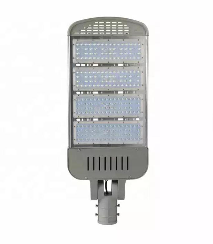
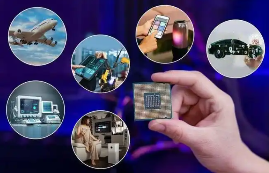
Which Industries Benefit Most from COB High-Power LED Module Copper Core PCB?
The COB High-Power LED Module Copper Core PCB is essential for industries that rely on high-power LED modules and pursue stable brightness and long-term reliability. Below are four key industries and real EBest case studies.
1. Industrial Lighting
Industrial warehouses and factories use high-power LED modules for bright, uniform lighting. Our COB High-Power LED Module Copper Core PCB ensures stable brightness even in high-temperature environments.
Case Study: A global industrial lighting manufacturer used our PCB for 200W LED high bay lights. The results showed: 30% less heat buildup and 98% brightness stability over 20,000 hours.
2. Architectural Lighting
Architectural lighting requires precise brightness control for building facades and public spaces. The high thermal conductivity of our PCB prevents color temperature shift and maintains lighting uniformity.
Case Study: An architectural firm used our COB High-Power LED Module Copper Core PCB for a 100-square-meter building facade project. The PCBs delivered uniform brightness with no visible light decay for 18 months.
3. Automotive Lighting
Automotive headlights and taillights use high-power LEDs, requiring PCBs that can withstand extreme temperature fluctuations. Our PCB can adapt to a temperature range of -40°C to +125°C, ensuring reliable operation in all climates.
Case Study: An automotive supplier used our PCB for LED headlights. After 10,000 thermal cycle tests (from -40°C to +85°C), the PCBs still maintained stable brightness and performance.
4. Outdoor Flood Lighting
Outdoor floodlights operate in harsh conditions (rain, extreme heat/cold) and require long-lasting brightness. Our COB High-Power LED Module Copper Core PCB is moisture-resistant and maintains stable thermal efficiency.
Case Study: A municipal government used our PCB for 150W outdoor floodlights. The PCBs delivered consistent brightness for 2 years with no maintenance issues.
How to Design a COB High-Power LED Module Copper Core PCB for Maximum Brightness Stability?
Designing a COB High-Power LED Module Copper Core PCB for maximum brightness stability requires focusing on thermal management, material selection, and layout design—here’s how to do it.
Choose the Right Copper Core Thickness
For high-power LED modules above 50W, we recommend using a 1.5-3.0mm copper core. Thicker cores improve heat dissipation, reduce LED chip temperature, and maintain brightness stability.
Optimize the Dielectric Layer Design
Use a high-insulation, thermally conductive dielectric layer (0.1-0.3mm). This ensures electrical safety while quickly transferring heat from LED chips to the copper core.
Optimize Layout for Heat Dissipation
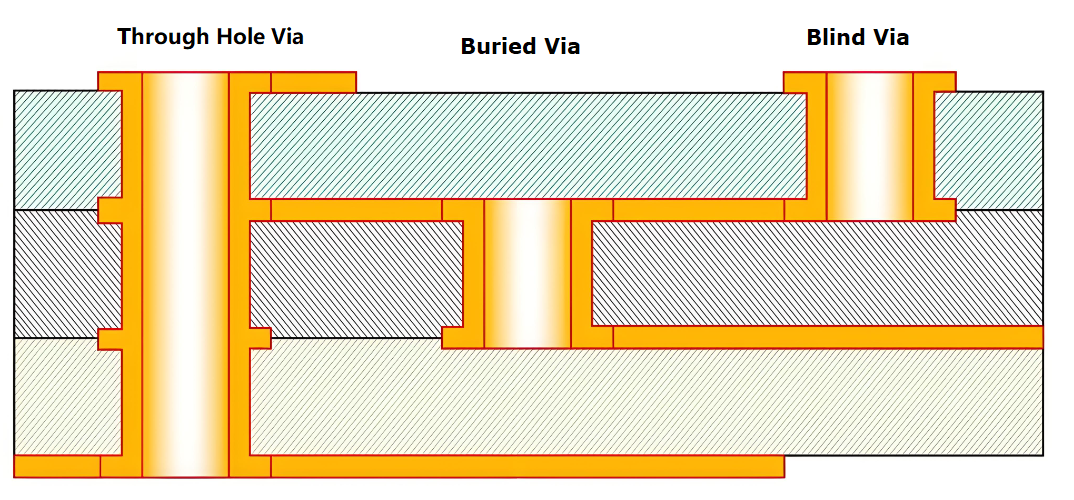
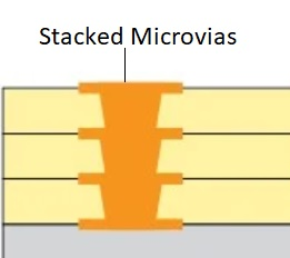
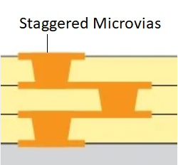
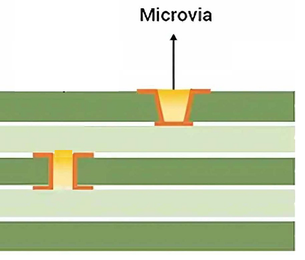
Evenly distribute LED chips across the PCB surface to avoid heat concentration; use large copper pads and thermal vias to transfer heat from the chip surface to the copper core.
Partner with a Reliable Manufacturer
Work with a manufacturer like EBest that specializes in COB High-Power LED Module Copper Core PCB. We offer design support to optimize your layout for maximum brightness stability.
What Quality Certifications Does EBest’s COB High-Power LED Module Copper Core PCB Have?
EBest’s COB High-Power LED Module Copper Core PCB meets global quality standards and holds multiple industry-recognized certifications. Below is a complete list of our certifications.
| Certification Name | Certification Body | Relevance to COB High-Power LED Module Copper Core PCB |
|---|---|---|
| ISO 9001:2015 | ISO (International Organization for Standardization) | Ensures stable quality management and production processes |
| UL 94 V-0 | UL (Underwriters Laboratories) | Fire-resistant, critical for LED modules in enclosed spaces |
| IPC-6012 | IPC (Association Connecting Electronics Industries) | Meets rigid PCB performance standards for high-power applications |
| RoHS | European Union (EU) | Environmentally friendly, free of hazardous substances |
| REACH | European Union (EU) | Complies with EU chemical safety standards for global distribution |
What Services Does EBest Offer for COB High-Power LED Module Copper Core PCB?
EBest provides end-to-end services for COB High-Power LED Module Copper Core PCB, from design to delivery, to ensure your project progresses seamlessly.
- Free Design Consultation: Our expert team helps you optimize your PCB design to enhance thermal conductivity and brightness stability.
- Rapid Prototyping: Complete prototyping in 3-5 days, allowing you to test the performance of your COB High-Power LED Module Copper Core PCB before mass production.
- Mass Production: Scalable production capacity to meet large-order requirements while ensuring consistent quality.
- Quality Inspection: 100% full inspection (thermal shock, continuity, insulation) for every PCB.
- After-Sales Support: 24/7 technical support to resolve any issues you encounter during PCB use.
How to Test the Thermal Conductivity of a COB High-Power LED Module Copper Core PCB?
Testing the thermal conductivity of your COB High-Power LED Module Copper Core PCB is a critical step to ensure it meets your project requirements. Follow these simple steps.
Step 1: Gather Test Equipment
You will need a thermal conductivity tester, temperature sensor, power supply, and your COB High-Power LED Module Copper Core PCB sample.
Step 2: Prepare the Sample
Cut the PCB into a standard size (100x100mm) and clean the surface to remove any debris that could affect heat transfer.
Step 3: Conduct the Test
Place the sample in the thermal conductivity tester, apply a stable heat source, measure the temperature difference across the PCB, and calculate using the formula: Thermal Conductivity = (Heat Flux × Thickness) ÷ Temperature Difference.
Step 4: Verify the Results
Compare the test result with your required specification (≥200 W/m·K for high-power applications). EBest’s PCBs are pre-tested, so you can trust they meet the stated thermal conductivity.
What Are the Common Myths About COB High-Power LED Module Copper Core PCB?
There are many misconceptions about COB High-Power LED Module Copper Core PCB—we debunk the most common ones to help you make informed decisions.
Myth 1: Copper Core PCBs Are Too Heavy for LED Modules
Fact: Our COB High-Power LED Module Copper Core PCB uses lightweight, high-purity copper cores (0.8-3.0mm) that are light enough for most LED module applications, including portable lighting.
Myth 2: High Thermal Conductivity Isn’t Necessary for Small LED Modules
Fact: Even small high-power LED modules (above 50W) generate enough heat to cause light decay. A copper core PCB ensures brightness stability, regardless of module size.
Myth 3: Copper Core PCBs Are Difficult to Manufacture
Fact: EBest has optimized production processes to efficiently manufacture COB High-Power LED Module Copper Core PCB, ensuring consistent quality and fast lead times.
Myth 4: Aluminum Core PCBs Perform as Well as Copper Core PCBs
Fact: Aluminum core PCBs have a thermal conductivity of only 10-20 W/m·K, much lower than the maximum 400 W/m·K of copper core PCBs, making them less effective for high-power LED modules.
FAQ: Common Questions About COB High-Power LED Module Copper Core PCB
Below are the most frequently asked questions about COB High-Power LED Module Copper Core PCB, with clear, direct answers to help you solve problems quickly.
Q1: How Long Does a COB High-Power LED Module Copper Core PCB Last?
A1: Under normal operating conditions (-40°C to +125°C), EBest’s COB High-Power LED Module Copper Core PCB has a service life of more than 50,000 hours. This matches the service life of high-power LED modules, ensuring no premature failure.
Q2: Can COB High-Power LED Module Copper Core PCB Be Customized to Specific Sizes?
A2: Yes, we offer fully customized COB High-Power LED Module Copper Core PCB in any size (from 50x50mm to 500x500mm) and thickness (0.8-3.0mm) to match your LED module design.
Q3: Does the COB High-Power LED Module Copper Core PCB Require Special Mounting?
A3: No, our COB High-Power LED Module Copper Core PCB uses standard mounting holes and dimensions, making it compatible with most LED module enclosures and fixtures. We can also customize mounting holes if needed.
Q4: How Does EBest Ensure Consistent Brightness Stability in Every PCB?
A4: Before shipping, we test every COB High-Power LED Module Copper Core PCB for thermal conductivity and brightness stability. Our quality control process includes thermal shock testing and brightness deviation measurement to ensure ≤2% deviation over 10,000 hours.
Q5: Can the COB High-Power LED Module Copper Core PCB Be Used for Outdoor Applications?
A5: Yes, our PCB is designed for outdoor use—it is moisture-resistant, corrosion-resistant, and can withstand extreme temperature fluctuations (-40°C to +125°C), making it ideal for outdoor floodlights and architectural lighting.
Q6: What Is the Minimum Order Quantity for COB High-Power LED Module Copper Core PCB?
A6: We accept small orders (minimum 10 units) for prototyping and large orders (1,000+ units) for mass production. This flexibility makes us suitable for both small projects and large-scale manufacturing.
Q7: How Quickly Can EBest Deliver Custom COB High-Power LED Module Copper Core PCB?
A7: Custom prototypes are delivered in 3-5 days, and standard custom orders are delivered in 7-10 days. Urgent orders can be fulfilled in 2-3 days with prior arrangement.
What Are the Latest Innovations in COB High-Power LED Module Copper Core PCB?
The COB High-Power LED Module Copper Core PCB industry is constantly evolving, with new innovations to improve thermal conductivity, brightness stability, and sustainability.
Innovation 1: Advanced Copper Alloys—We use high-purity copper alloys to boost thermal conductivity up to 400 W/m·K, improving heat dissipation and brightness stability.
Innovation 2: Thin-Film Dielectric Layers—New thin-film dielectric materials reduce thermal resistance, transferring heat faster from LED chips to the copper core.
Innovation 3: Sustainable Manufacturing—We use eco-friendly materials and processes to produce COB High-Power LED Module Copper Core PCB that meet RoHS and REACH standards, reducing environmental impact.
Why Is EBest the Trusted Supplier for COB High-Power LED Module Copper Core PCB?
EBest is the trusted supplier for COB High-Power LED Module Copper Core PCB because we combine quality, reliability, and expert support to meet your project needs.
We have years of experience manufacturing high-performance PCBs for high-power LED modules, with a proven track record of serving global clients in the industrial, architectural, automotive, and outdoor lighting industries.
Our commitment to quality, on-time delivery, and 24/7 support makes us the top choice for businesses that demand the best COB High-Power LED Module Copper Core PCB for brightness stability and thermal performance.
We provide high-quality COB High-Power LED Module Copper Core PCB – High Thermal Conductivity for Brightness Stability. If you need reliable, high-performance PCBs for your LED modules, please place your order with EBest. Our email is sales@bestpcbs.com, and our team is ready to assist you with all your requirements.