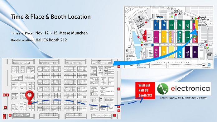
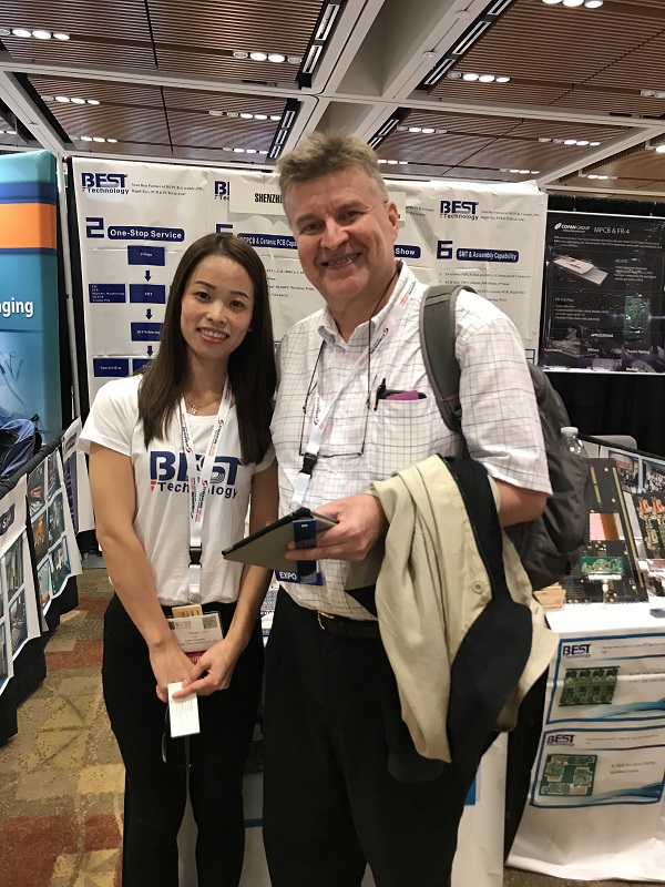
Exciting News! EBest Circuit (Best Technology), a leading PCB assembly manufacturer from China, will be exhibiting at Electronica Munich 2024 in Germany. Join us at Booth No. 212 (Hall C6) from November 12 – 15, 2024 (Western Time). If you missed us at PCB West or AEMS, this is your chance!
At our booth, you’ll have the opportunity to explore our advanced PCB manufacturing and assembly technologies. For reference, here is a booth location detail.
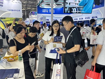
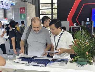
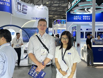
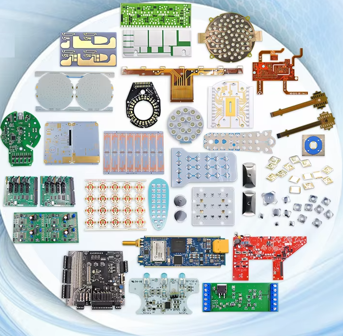
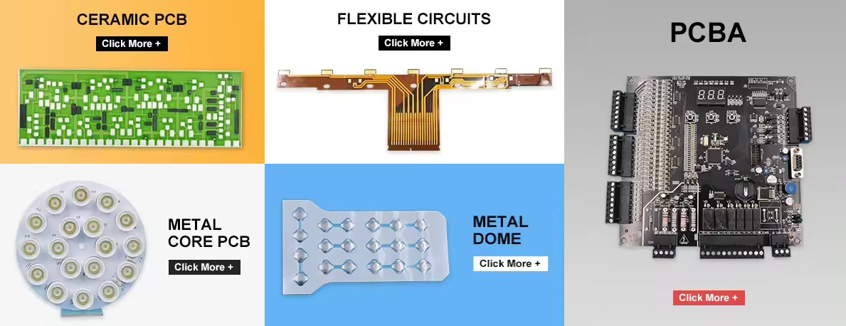
Actually, we have participated such exhibitions for several times, like PCB west, electronica in China, AEMS and so on. Here are some pictures:
In the exhibition, our team of experts will be available to share in-depth knowledge about PCB assembly, from prototyping to low and high-volume production. We invite all interested professionals/engineers to visit and discover our capabilities in flexible circuit boards, rigid-flex circuits (2 to 50 layers), copper weights from 1/2 OZ to 30 OZ, and ultra-thin PCBs (0.15mm FR4) to heavy copper options. EBest Circuit (Best Technology) offers a full turn-key service including component sourcing, board fabrication (FPC, PCB, MCPCB, Ceramic PCB), final assembly, programming, testing, and more.
Additionally, we’ll showcase our metal dome products, widely used as tactile switches in conjunction with PCBs, flex circuits, or membrane keypads. Available in four varieties—four-leg domes (5mm-20mm), triangle domes (4mm-12mm), round domes (4mm-16mm), and oblong domes (3.7mm-58.1mm)—our metal domes come with or without adhesive (dome arrays).
We welcome you to explore how we manage component wastage and boost efficiency, helping you save time, money, and resources.
About Electronica Munich
Electronica is the world’s premier trade show for electronic components, systems, and applications, showcasing cutting-edge innovations and developments across industries. It’s the perfect place to learn about the latest trends in PCB manufacturing, power engineering, system peripherals, and EMS.
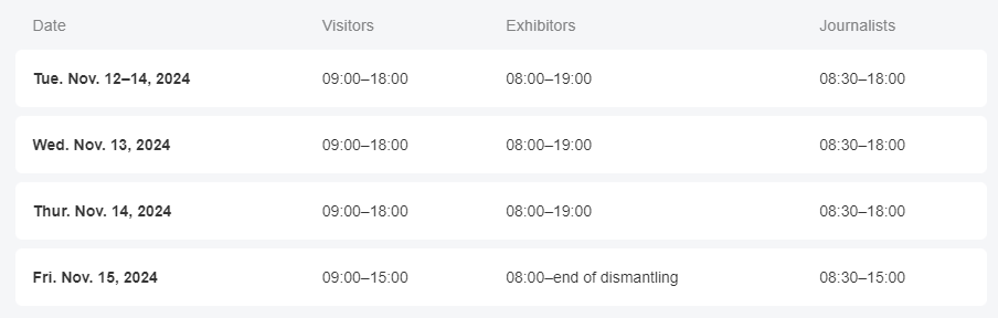
Openning Hours of Electronica Munich 2024
Please keep in mind that your visitor ticket does not allow you to reenter the fair and will not open the turnstiles a second time if you leave the fair!
For the visit/travel information about transportation, welcome to click electronica 2024 website or click here.
Don’t miss out! We look forward to seeing you at Booth 212 from November 12 to November 15, 2024 (Western Time).
Can you use AC in PCB?AC can be used in PCB boards. PCB boards are designed to support the use of AC, and the functions of AC can be realized through proper circuit design and component selection.
Can you use AC in PCB?
The use of AC in PCB boards requires consideration of the characteristics of AC. The current magnitude and direction of AC change continuously over time, which requires the components and layout on the PCB to adapt to such changes. For example, components such as inductors and capacitors play an important role in AC circuits, and their parameters and layout need to be carefully designed to achieve the desired circuit performance.
Specifically, AC circuit design on PCB boards includes selecting appropriate components, layout, and routing. For example, using test instruments such as LCR digital bridges can measure the parameters of components in AC circuits to ensure that the performance of the circuit meets the design requirements. In addition, reasonable ground routing and layout can reduce signal interference and ensure the stable transmission of AC.
Is the circuit board DC or AC?
Circuit boards can transmit both direct current and alternating current. In modern electronic products, we use alternating current for power supply, so most circuit boards are also designed to transmit alternating current. Of course, in some special application scenarios, some circuit boards also need to transmit direct current. Whether transmitting direct current or alternating current, the circuit board needs to meet the requirements of the transmitted current.
What is the PCB in AC?
The alternating current in PCB refers to the current whose direction changes periodically, that is, alternating current (AC). The application of alternating current in PCB is mainly reflected in power conversion and power transmission. PCB power supply usually converts AC into stable direct current (DC) output to meet the demand of electronic equipment for stable power supply. PCB power supply converts AC into the required DC through components such as transformers, rectifiers, filters and voltage regulators, and provides stable power output.
How to calculate the bandwidth of AC in PCB traces
The calculation of AC PCB trace width can be performed by the following formula: W = (I / J) * K, where W represents the trace width, I represents the current, J represents the current density, and K represents a coefficient related to materials and processes. This formula shows that the trace width is related to the current, current density, and material properties.
AC in PCB Design Guide
Current Carrying Capacity: The width of a trace directly affects its ability to handle current without exceeding temperature limits or causing excessive voltage drop. Impedance Control: In high-frequency applications, maintaining controlled impedance is critical for signal integrity. Trace width, trace spacing, and dielectric properties affect the characteristic impedance of the transmission line. Heat Dissipation: Adequate trace width helps to effectively dissipate heat, preventing thermal issues such as trace delamination or solder joint failure. Voltage Drop: Narrower traces exhibit higher resistance, resulting in increased voltage drop along the length of the trace. By adjusting the trace width, the voltage drop can be minimized. Manufacturability: The PCB manufacturing process imposes restrictions on the minimum trace width, and designers must balance performance requirements with manufacturability constraints. 2. Minimum Trace Width: Most manufacturers have a minimum trace width of 6mil or 0.152mm, and typically use traces of 0.254-0.3mm. Material and Process Deviations: Due to the possibility of material and process deviations in the actual PCB manufacturing process, a certain margin needs to be left when calculating the line width. Signal Integrity Simulation: Perform signal integrity simulations to ensure impedance is controlled and signal degradation due to reflections, crosstalk, or transmission line effects is minimized
AC in PCB wiring
The current trend is that the power supply voltage is getting lower and lower (especially for highly integrated digital devices), the space occupied is getting smaller and smaller, the weight is getting lighter and lighter, and the efficiency is getting higher and higher, which requires the precise design of the power supply circuit starting from the PCB.
Safety distance includes electrical clearance (spatial distance), creepage distance (surface distance) and insulation penetration distance…
Electrical clearance: the shortest distance between two adjacent conductors or one conductor and the adjacent motor housing surface measured along the air.
Creepage distance: the shortest distance between two adjacent conductors or one conductor and the adjacent motor housing surface measured along the insulation surface.
Determination of electrical clearance:
The distance can be determined according to the measured working voltage and insulation level
The electrical clearance size requirements of the primary side line are shown in Table 3 and Table 4
The electrical clearance size requirements of the secondary side line are shown in Table 5
But usually: Primary side AC part: L-N ≥ 2.5mm before the fuse, L.N PE (earth) ≥ 2.5mm, no requirements are made after the fuse is installed, but a certain distance should be maintained as much as possible to avoid short circuit damage to the power supply.
Primary side AC to DC part ≥2.0mm
Primary side DC ground to earth ≥2.5mm (primary side floating ground to earth)
Primary side to secondary side ≥4.0mm, components connected between primary and secondary sides
Secondary side gap ≥0.5mm
Secondary side ground to earth ≥1.0mm
Note: Before determining whether it meets the requirements, the internal parts should be applied with a force of 10N and the outer shell with a force of 30N to reduce the distance so that the space distance still meets the requirements under the worst case.
Determination of creepage distance:
Based on the working voltage and insulation level, the creepage distance can be determined by looking up Table 6
But usually: (1), primary side AC part: L-N ≥2.5mm before the fuse, L.N earth ≥2.5mm, no requirement is required after the fuse, but try to keep a certain distance to avoid short circuit damage to the power supply.
(2) Primary side AC to DC part ≥2.0mm
(3) Primary side DC ground to ground ≥4.0mm such as primary side ground to earth
(4) Primary side to secondary side ≥6.4mm, such as optocoupler, Y capacitor and other components, the foot spacing ≤6.4mm needs to be slotted.
(5) Secondary side parts ≥0.5mm
(6) Secondary side ground to earth ≥2.0mm or more
(7) Transformer two-stage ≥8.0mm or more
Insulation penetration distance:
It should meet the following requirements according to the working voltage and insulation application:
For working voltage not exceeding 50V (71V AC peak or DC value), there is no thickness requirement;
The minimum thickness of additional insulation should be 0.4mm;
When the reinforced insulation is not subjected to any mechanical stress that may cause deformation or performance degradation of the insulating material at normal temperature, the minimum thickness of the reinforced insulation should be 0.4mm. If the insulation provided is used in the protective casing of the equipment and will not be bumped or scratched during maintenance by the operator, and any of the following conditions apply, the above requirements do not apply to thin insulating materials regardless of their thickness;
For additional insulation, at least two layers of material are used, each of which can pass the dielectric strength test for additional insulation; or:
For additional insulation composed of three layers of material, any combination of two layers of material can pass the dielectric strength test for additional insulation; or:
For reinforced insulation, at least two layers of material are used, each of which can pass the dielectric strength test for reinforced insulation; or:
For reinforced insulation composed of three layers of insulating material, any combination of two layers of material can pass the dielectric strength test for reinforced insulation.
Points to note about wiring process:
Flat components such as capacitors must be flat without glue.
If the distance between two conductors can be shortened by applying a force of 10N, which is less than the safety distance requirement, glue can be used to fix the part to ensure its electrical clearance.
When laying PVC film inside some shell equipment, attention should be paid to ensuring the safety distance (pay attention to the processing technology).
When fixing the parts with glue, be careful not to leave foreign matter such as glue wire on the PCB board.
When processing parts, insulation damage should not be caused.
Requirements for flame-proof materials:
Heat shrink tubing V-1 or VTM-2 or above; PVC tubing V-1 or VTM-2 or above
Teflon tubing V-1 or VTM-2 or above; plastic materials such as silicone sheets, insulating tape V-1 or VTM-2 or above
PCB board 94V-1 or above
Regarding insulation level
(1) Working insulation: insulation required for normal operation of equipment
(2) Basic insulation: insulation that provides basic protection against electric shock
(3) Supplementary insulation: independent insulation applied in addition to basic insulation to protect against electric shock in case of basic insulation failure
(4) Double insulation: insulation consisting of basic insulation plus supplementary insulation
(5) Reinforced insulation: a single insulation structure that provides the same level of protection against electric shock as double insulation under the conditions specified in this standard
The applicable situations of various insulation are as follows:
A. Operational insulation
a. Between parts with different voltages
b. Between ELV circuits (or SELV circuits) and grounded conductive parts.
B. Basic insulation
a. Between parts with dangerous voltages and grounded conductive parts;
b. Between SELV circuits with dangerous voltages and grounding-dependent;
c. Between the primary power conductor and the grounded shield or the core of the main power transformer;
d. As part of double insulation.
C. Supplementary insulation.
a. Generally speaking, between accessible conductive parts and parts that may carry dangerous voltages after basic insulation is damaged, such as:
Ⅰ. Between the surface of handles, knobs, handles or similar objects and their ungrounded axis.
Ⅱ. Between the metal casing of the second category equipment and the outer skin of the power cord passing through this casing.
Ⅲ. Between the ELV circuit and the ungrounded metal casing.
b. As part of double insulation
D. Double insulation
Double insulation Reinforced insulation
Generally speaking, between the primary circuit and
a. between accessible ungrounded conductive parts, or
Under normal working conditions, the AC peak value between conductors or between any conductors does not exceed 42.4V or the DC value does not exceed 60V.
SELV circuit: safety extra low voltage circuit.
A properly designed and protected secondary circuit so that under normal conditions or single fault conditions, the voltage between any two accessible parts, and between any accessible parts and the protective grounding terminal of the equipment (only for Class I equipment) will not exceed the safety value.
TNV: communication network voltage circuit
Under normal working conditions, the circuit carrying communication signals
Difference between direct current and alternating current
The main differences between DC and AC include direction and polarity, voltage change, current loss, transformer use, and application scenarios.
Direction and polarity:
DC: The direction of the current remains unchanged, and the electrons flow from the positive electrode to the negative electrode.
AC: The direction of the current changes periodically, and the electrons flow back and forth between the positive and negative electrodes. Voltage change:
DC: The voltage remains constant and does not change over time.
AC: The voltage magnitude and direction change periodically over time. For example, the mains is an AC with a sine waveform.
Current loss:
DC: Fault losses are relatively small.
AC: There is capacitive current, and there is capacitive current in the transmission line. Transformer use:
DC: The voltage cannot be changed using a transformer.
AC: The voltage can be changed using a transformer, which is suitable for boosting voltage to reduce losses during long-distance transportation.
Application scenarios:
DC: Suitable for low-voltage electrical appliances and occasions that require stable current. Alternating current: Suitable for household and industrial use, using transformers to change voltage to suit different needs.
FAQ About AC in PCB
FAQ About AC in PCB
Q: The relationship between PCB current and line width. Is the current divided into AC or DC? A: The relationship between PCB current and line width is not divided into AC or DC. In terms of the nature of the lines on the PCB, the lines are all made of copper materials, and both AC and DC can pass. However, how much current can pass depends on the cross-sectional area of the line on your PCB. That is, line width x thickness of the copper foil of the line. If the cross-sectional area of the line is small, only small current signals can pass, and if the cross-sectional area is large, large current signals can pass. This signal can be AC or DC. Not just 1mm, any line width can pass DC or AC signals.
Q: There is a packaged device, and there are 2 pins in the device that need to be connected to the live wire and neutral wire of 220V AC respectively. So how to deal with this power line when drawing the PCB? Are there any size requirements for pads, wires, etc.? Are there any protective measures required? Is it not possible to directly add pads to connect to the pin pads of the device? A: It is best to mill a groove between the neutral wire and the live wire, and choose the thickness of the wire according to the current. When the current is large, you can put a tin layer on the wire, and the pad should be slightly larger.
Q: The grounding of the PCB circuit board design is also the negative pole. What is the difference between the grounding here and the AC grounding?
A: The concept of the circuit board ground is somewhat different from that of the power supply system. The power supply system refers to the earth, that is, the terminal with the same potential as the earth.
The ground in the circuit board is just a common terminal of a potential, which can be positive or negative, depending on the needs of the designer. It’s just that everyone is used to and assumes that the negative pole is the common terminal, that is, the ground. The circuit board ground is not necessarily connected to the earth.
But it must be connected to the earth when EMI filtering is required.
Q: Should all GNDs on the PCB board be connected? There is a terminal (screw type) with two terminals marked as V1+ and V1- on the PCB schematic. Should V1- be connected to the power supply ground? But I used a multimeter to measure why V3- is not connected to other GNDs on the board?
So how do you connect the ground and 10V of the power supply to the V1+ and V1- ends of the terminal?
A: Not all ground wires on the board are connected together. The ground wires are divided into analog ground and digital ground, just like the ground wire in DC and the ground wire in AC cannot be connected together. That is to say, there is a ground wire that is specifically used for power supply, and there is a ground wire that is specifically used for signals (shielding signal interference). These two ground wires cannot be connected together. In addition, you mentioned V1+ and V1-, and V1- should not be considered a ground wire. Generally, the signal represented by this method is a differential signal, that is, the V1 signal is differentially divided into V1+ and V1-, which can reduce external interference and transmit farther. Finally, V1+ and V1- are integrated into the V1 signal. You need to figure out whether the V1+ and V1- of the terminal are used for power supply. If they are used for power supply, then V1+ is the positive pole. V1- is the negative pole. Since you didn’t show us the picture, you can’t just connect it randomly. The circuit board needs to connect not only power but also signals, depending on how your board is made.
EBest Circuit (Best Technology), a leading PCB and PCBA manufacturer based in China, is excited to announce our participation at the Anaheim Electronics & Manufacturing Show (AEMS) 2024. The event will take place in Anaheim, California, and we invite you to visit us at Booth No. 108 from October 2 to October 3, 2024 (Western Time). The exhibition venue is located at 800 W Katella Ave, Anaheim, CA. Having been part of this show for several years, we look forward to showcasing our latest innovations and discussing our comprehensive PCB manufacturing and assembly solutions.
At our booth, attendees will have the opportunity to engage with our experts and learn about a wide range of services, including PCB prototyping and low-to-high volume production. We’ll be showcasing products like flexible circuit boards ranging from 10mm to 1,500mm, rigid-flex circuits up to 50 layers, and PCBs with copper thickness from 1/2 OZ to 30 OZ. Visitors can also explore ceramic PCBs, such as thick film, thin film, DPC, DBC, HTCC, AMB, and LTCC varieties. In addition, we will be unveiling new products including copper/aluminum busbar PCBs, transparent/PI/rubber silicone flexible heating films, and semi-flexible PCBs.
EBest Circuit (Best Technology) is proud to offer one-stop services covering everything from components sourcing, PCB fabrication (FPC, PCB, MCPCB, Ceramic PCBs), to final assembly with programming and testing.
Be sure to visit us at Booth 108 to see how we optimize efficiency, reduce component wastage, and help you save on time, money, and energy.
rigid-flex printed circuit board ,Rigid flex pcb manufacturer. More than 5 years design team of 10 people. Quick proofing within 1 week. A 3,000-square-meter factory for small batch to mass production and assembly.
What is a rigid flex pcb?
Rigid flex pcb,rigid-flex printed circuit board,Rigid flex circuit are a hybrid construction flex circuit consisting of rigid and flexible substrates which are laminated together into a single structure. Each layer of rigid-flex circuit are electrically interconnected by plated through holes (PTH), which is different from a flexible circuit with FR4/PI stiffener on top or bottom of flex circuit only by the means of presensive or thermal senstive adhesive only, no PTH.
Rigid-flex PCBs can be divided into single-sided boards, double-sided boards and multi-layer boards according to the number of conductive circuit layers. Multi-layer boards usually contain multiple rigid layers and flexible layers, and the circuits are connected and interconnected through interlayer connections.
Is Rigid flex PCB reliable?
Design and manufacturing efficiency: Designers of rigid-flex boards can use a single component to replace a composite printed circuit board connected by multiple connectors, multiple cables and ribbon cables, which not only has stronger performance and higher stability, but also limits the scope of the design to one component, optimizing the available space by bending and folding the lines like a stacked paper swan.
Space and weight optimization: In PCB prototyping for consumer electronics, the use of rigid-flex boards not only maximizes space use and minimizes weight, but also greatly improves reliability, eliminating many needs for solder joints and fragile and fragile wiring that are prone to connection problems. The design of this circuit board allows the size and weight of equipment and systems to be reduced while maintaining functionality.
High stress environment adaptability: Rigid-flex boards also have high impact resistance and can survive in high stress environments, which makes it widely used in military, aviation and medical equipment.
Excellent electrical performance: Rigid-flex boards provide excellent electrical performance, and good thermal conductivity makes components easy to cool. The lower dielectric constant of the flexible part allows for fast transmission of electrical signals, and the PI substrate has a higher glass transition temperature or melting point, which allows the components to operate well at higher temperatures.
Assembly reliability: Rigid-flex boards reduce the hardware required for traditional rigid boards and flexible boards to be connected, such as traditional jumper sockets, etc., and can provide higher assembly reliability.
What is the difference between rigid flex and semi flex?
Definition and structure Rigid-flexible board: It is a combination of soft board and hard board, that is, a thin layer of flexible bottom layer and rigid bottom layer are combined and laminated into a single component to form a circuit board1. It changes the traditional flat design concept and expands it to a three-dimensional space concept. It has both rigid layer and flexible layer and is a multi-layer printed circuit board. Semi-flexible board: It is a PCB used in the field of static bending obtained by combining controlled deep milling or rigid-flexible board processing technology (such as milling cover or opening window, etc.) in the standard hard board processing process2. It often uses FR4 material, first processes the PCB according to the normal process, and then mills the middle part that needs to be bent to make it flexible.
Flexibility and application Rigid-flexible board: It has higher flexibility and can be bent, folded or rounded, and then integrated into various products, such as aerospace equipment, military aircraft, high-end medical equipment, digital cameras, portable cameras and high-quality MP3 players. Semi-flexible board: Although it can be bent or curved, its flexibility is not as good as that of rigid-flexible board. It is mainly used in situations where static bending is required, such as endoscopes in medical equipment, injection needle tip protection circuit boards, and medical equipment temperature control circuit boards.
Processing and cost Rigid-flexible board: Due to the mixed use of multiple materials and multiple production steps, its processing time is longer and the production cost is higher. Semi-flexible board: Although its processing process is also more complicated, its processing cost is lower than that of rigid-flexible board, and it is more suitable in some applications.
Features and advantages Rigid-flexible board: It has stronger performance and higher stability, can reduce space and weight, and improve the reliability of connection.
Semi-flexible board: It has the advantages of low cost, good dimensional stability, bendable three-dimensional installation to reduce space, and reduce the number of interfaces during assembly to improve reliability.
how do they add rigid layers to flex pcb?
Design layout: Before starting the manufacturing process, the PCB design layout is first carried out to determine the location and connection method of the components.
Substrate preparation: Clean the laminate containing the copper layer to prepare for the subsequent manufacturing process.
Pattern generation: The generation of circuit patterns is completed by screen printing or photo imaging.
Etching process: The laminate with the circuit pattern is soaked in an etching tank or sprayed with an etchant solution for etching.
Mechanical drilling: Circuit holes, pads and via patterns are drilled using a precision drilling system or technology, such as laser drilling technology.
Copper plating process: Deposit the required copper in the plated vias to establish electrical interconnections between layers.
Covering layer application and lamination: Apply the covering layer material (such as polyimide film) and adhesive, and laminate under specific temperature, pressure and vacuum limits to ensure proper adhesion of the covering layer.
Apply stiffeners: Apply local additional stiffeners before additional lamination processes as required by the board design.
Flexible board cutting: Cut flexible boards from production panels using hydraulic punching methods or specialized punching knives.
Electrical testing and verification: Conduct electrical testing in accordance with IPC-ET-652 guidelines to confirm that the insulation, connection, quality, and performance of the circuit board meet the requirements of the design specifications.
What are the disadvantages of rigid flex PCB?
Material damage or breakage: The flexible materials used in rigid-flex boards are susceptible to flexure and bending. Long-term use or improper handling may cause damage or breakage of the flexible part, resulting in an open circuit.
Poor welding: The manufacture of rigid-flex boards requires welding processes. If the welding is poor or the solder joints are of poor quality, it may cause loose connections or solder joints to fall off, resulting in an open circuit.
Excessive bending or stretching: Excessive bending or stretching during use may cause the connection wires or wires of the flexible part to be stretched excessively and break, causing an open circuit.
Design defects: If the design of the rigid-flex board is unreasonable or defective, such as insufficient design of the overbending area or too small bending radius, the material of the flexible part may be damaged by excessive stress, resulting in an open circuit.
Environmental factors: Under different environmental conditions, it may be affected by factors such as temperature, humidity, and chemicals. Long-term use in harsh environments may cause material aging or corrosion, resulting in an open circuit.
Damage during assembly: During the assembly process, improper operation or external force may cause damage to the connecting wires or wires of the flexible part, resulting in an open circuit.
Application fields of rigid flex PCB
Automotive electronics: Rigid-flex boards are widely used in automotive electronic systems such as dashboards, navigation systems, and in-car entertainment systems in the automotive industry. Their flexibility and high reliability enable them to adapt to the complex spatial layout and vibration environment inside the car.
Medical equipment: In the field of medical equipment, rigid-flex boards also have important applications, such as medical monitoring equipment, medical imaging equipment, etc. Its flexible part can adapt to different equipment shapes and size requirements, while having stable circuit connection performance.
Aerospace field: Rigid-flex boards are usually used in aircraft dashboards, navigation systems, communication equipment, etc. in the aerospace field. Due to their light, thin and flexible characteristics, rigid-flex boards have become an ideal choice for aerospace equipment.
Smart wearable devices: With the rapid development of smart wearable devices, rigid-flex boards are widely used in products such as smart watches and health monitoring equipment. They can be combined with curved display screens, sensors and other components to achieve a more humanized design.
Industrial control field: In the field of industrial automation control, rigid-flex boards are often used in PLC controllers, robot control systems, sensor interfaces, etc. Its flexibility and reliability ensure the stable operation of the equipment in harsh environments.
Rigid flex pcb manufacturer
rigid flex pcb.rigid-flex printed circuit board,Rigid flex circuit are a hybrid construction flex circuit consisting of rigid and flexible substrates which are laminated together into a single structure. Each layer of rigid-flex circuit are electrically interconnected by plated through holes (PTH), which is different from a flexible circuit with FR4/PI stiffener on top or bottom of flex circuit only by the means of presensive or thermal senstive adhesive only, no PTH.
Multilayer circuitry-from 3 to 14+ layers Min LW/LS: 4mil/4mil Adhesive-based and adhesiveless constructions, including thermoplastic and thermoset stiffener attachment. Polyimide substrates: 1/2mil – 4mil Copper: 1/3OZ – 2OZ, RA or ED type Stiffeners include Polyimide (0.075-0.20mm), FR4 (0.15-2.0mm), and punched or formed metal parts (0.075-1.0mm) Low-cost, conventional fabrication and lamination completed with PTH based plating Screened inks, photo-imageable soldermasks, or laminated coverlay dielectrics Surface finishes: ENIG, electroplated nickel/gold, immersion silver, tin, EMI Shielding
how to design flex rigid pcb?
Rigid-Flex Circuit Design Guidelines
To form a rigid-flex, follow these considerations to ensure the best results.
Considerations When Designing Rigid-Flex Circuits
To produce a rigid-flex PCB with unmatched quality and functionality, you must follow the correct manufacturing specifications. This is the set guidelines and standards that manufacturers must consider when designing and manufacturing flexible circuit boards.
Determine Manufacturing Process and Materials Beforehand
Depending on the flexibility you require, you need to decide beforehand what materials to use and the methods to use. Example; When the board you are designing only needs to be folded during manufacturing and thereafter be in a fixed position without bending, you can decide the following
Copper type and grade
Manufacturing method
Number of layers to be used.
On the other hand, if the board is for an application with frequent movement, vibration, and impact, you must be clear in choosing the following:
Copper Coils
Adhesives and
Number of Layers
Place Copper Traces at Right Angles to Rigid-Flex
Copperworks is a great fit when placed on the right edge of the board. Avoid bending copper traces at corners as it will pull stress and may not create the best bend. For PCB flex that requires bending, use sharp radius bends to avoid smudging copper traces.
Provide adequate pad support for exposed copper
Repetitive stress from frequent bending can cause copper on the circuit to break away from the polyimide substrate. Support exposed copper with pads to prevent separation.
Use hatched polygons
Hatched polygons instead of solidified copper help maintain the flexibility of flexible PCBs.
Leave at least 1/2mm gap between copper ring and adjacent vias
1/2mm helps avoid fatigue caused by frequent bending. Placing vias in fixed areas of the board helps avoid frequent movement and bending, resulting in the best rigid-flex.
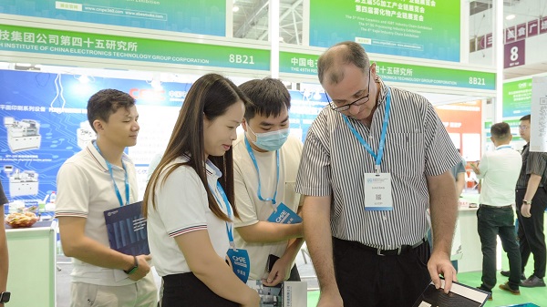
During July 8th to 10th, EBest Circuit (Best Technology) had an exhibition at the Electronica China 2024, and now, we are so excited to share that we had an incredible time! It was our first time at this event, and we believe it is not the last time.
It is must to say that the Electronica the perfect place for us to show off our cutting-edge PCB products. Our booth was buzzing with visitors curious about our advancements in metal core PCBs, ceramic PCBs, flexible PCBs and PCB design. We were thrilled with the positive feedback and the high interest in what we had to offer.
The exhibition wasn’t just about our products; it was also about making meaningful connections. We got to chat with industry experts, potential clients, and fellow exhibitors, discussing the latest trends and exploring possible collaborations. These conversations were incredibly valuable, and we’re excited to keep these relationships growing.
At this exhibition, EBest Circuit (Best Technology) also attracted the attention of authoritative media such as CCTV (China Central Television). It is a big and famous media in China. CCTV reporter visited our booth and conducted an interview with our founder, Peter. During the interview, Peter introduced the company’s latest products and technical advantages in detail, and shared the successful experience and future development plan of Best in the industry.
We want to send a huge thank you to all the friends and visitors who stopped by our booth. Your support and interest mean so much to us. Your enthusiasm for our products has motivated us to keep pushing the boundaries and coming up with even better solutions.
If you didn’t get a chance to see us at Electronica China 2024, don’t worry! We’ve got more exciting exhibitions lined up. You can catch us at PCB West in October and in Munich, Germany in November. We can’t wait to meet more industry pros and show off our latest innovations at these events.
EBest Circuit (Best Technology)’s debut at Electronica China 2024 was a big success. We’re so grateful for the opportunity to share our products and connect with the industry community. Thanks again to everyone who visited our booth. We look forward to seeing you at our upcoming exhibitions!
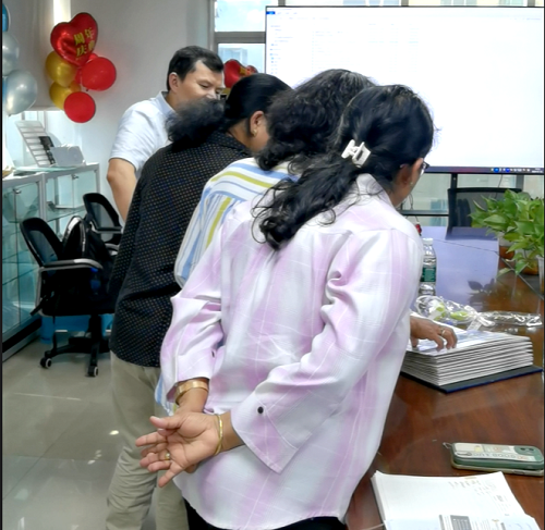
On July 3rd, 2024, we had India customers visit our office and factory. All our staff of our customer warmly welcome the guest from afar.
Our sales manager Peter, along with Connie and Marina, gave a detailed introduction to our main business and product expertise. They talked about our strict quality control, careful selection of PCB board materials, advanced production equipment, and mature manufacturing processes. Our guests seemed quite impressed with how thorough we are in ensuring top-notch quality.
Actually, we’ve been working with this customer for several years now, and it’s been a fantastic journey of building trust and collaboration. This visit was a great chance to dive into a new PCB project and show off our latest innovations, including electric heating films, ceramic PCBs, and bendable aluminum PCBs.
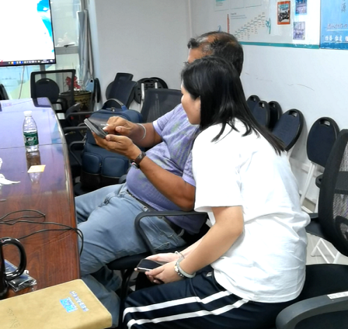
When checking the sample books, the customers specially mentioned the blind vias and checked the related products for many times. It looks like they are extremely interested in this technology. You know, blind vias, buried vias, through hole vias, micro vias and thermal vias are always our strengthens.
Next day, Connie will be taking our guests on a tour of our metal dome and dome array factory. It’s always exciting to show our partners the heart of our operations and let them see firsthand the dedication and precision that goes into our work.
EBest Circuit (Best Technology) is a one-stop PCB and PCBA service provider in China and Vietnam. “High mix, Low-Middle Volume, High Quality and Fast Delivery” is our advantages. Custom PCBs available in our company as well. You can get high-quality PCB board and PCBA at a very transparent price. For more information, feel free to contact us at any time.
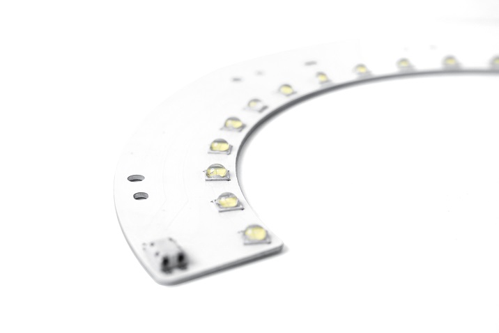
Nowadays, LED lighting has become increasingly popular in our daily life. With its rapidly rise in popularity, the term LED PCB has become commonplace. LED PCB also referred to as LED circuit board, LED aluminum PCB, or simply LED PCB board. Today, our team will share some informational knowledges about LED PCB circuit board, let’s keep reading if you are interested!
What is a LED PCB Circuit Board?
A LED PCB circuit board is a unique type of board crafted to hold and connect light-emitting diodes (LEDs). They are specially designed for lighting applications, like LED car headlights, pool lighting, UV LED, hotel lighting, grow light, high bay lights, stair lights, supermarket lighting, street light, etc. They are used almost everywhere. These boards provide the support and connections needed for LEDs to function efficiently and last longer. They are crucial in areas like lighting, automotive, and electronics, thanks to their ability to manage heat effectively and enhance the lifespan of LEDs.
What are the Different Types of LED PCB?
LED PCB boards are preferred over traditional lighting methods like fluorescent and incandescent bulbs. There are in total five types of LED PCBs, each designed for specific applications:
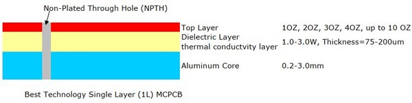
Aluminum based LED PCB
An LED PCB board, often made of aluminum alloy, serve as the base for mounting LEDs. This is the most common type of LED PCB, since it has good thermal management and cost-effective compared to other materials. The thermal conductivity of aluminum can be 1.0-3.0W/m.k, it can meet the almost heat requirements of low-middle power applications, like streetlights and floodlights. Additionally, EBest Circuit (Best Technology) developed a new product called semi-flexible aluminum PCB for specific device. It can be bent and folded when necessary.
Copper core LED PCB
Copper core LED circuit board can be divided into two types: normal copper core LED PCB and thermoelectric separation copper-based LED PCB. The copper material has higher thermal conductivity than that of aluminum, and it can up to 400W/m.k when made by thermoelectric separation technology. Copper based LED PCB board commonly used in high power devices like new energy vehicles.
Ceramic LED PCB
Ceramic LED PCB boards are made from ceramic substrates like aluminum oxide (Al2O3) or aluminum nitride (AlN). They have superior thermal management, and it can withstand extreme environment when used in high-temp and low temperatures. Ceramic substrates can handle high power and thermal cycling better than other materials, making them ideal for automotive, aerospace, and high-power LED applications.
FR4 LED PCB
FR4 LED PCB boards are made from woven fiberglass cloth with an epoxy resin binder, which provides good mechanical strength and insulation properties. FR4 is a widely used material for general-purpose PCBs due to its cost-effectiveness and versatility. While it has lower thermal conductivity (around 0.3W/m.k) compared to aluminum or copper, FR4 LED PCBs are suitable for low to medium power applications where thermal management is less critical. These PCBs are commonly used in consumer electronics, LED displays, and indoor lighting.
Flexible LED PCB
Flexible LED PCB boards are constructed using flexible plastic substrates like polyimide or polyester. This flexibility allows the PCBs to be bent, folded, and shaped to fit various applications. Flexible LED PCBs are ideal for products that require dynamic or complex designs, such as wearable electronics, flexible displays, and medical devices. Despite their lower thermal conductivity compared to rigid PCBs, flexible LED PCBs offer unique design advantages and are increasingly used in innovative LED applications.
What are the Benefits of Using Aluminum LED PCB Boards?
Aluminum LED PCB boards offer numerous advantages that other materials cannot achieved.
1. Better Heat Management: LED PCBs, particularly aluminum ones, help in cooling LEDs, preventing overheating and extending their lifespan.
2. Compact and Light: These boards are small and lightweight, making them perfect for applications with space and weight constraints.
3. Dimensional stability: Aluminum LED PCB board has good dimensional stability compared with flexible LED PCBs. And it has low CTE during the manufacturing.
4. Cost-Effective: Producing aluminum LED PCBs is relatively affordable, making them a budget friendly option for various applications.
5. Versatile: Available in different shapes and sizes, Aluminum LED PCBs can be customized to meet specific needs, enhancing their usefulness in various scenarios.
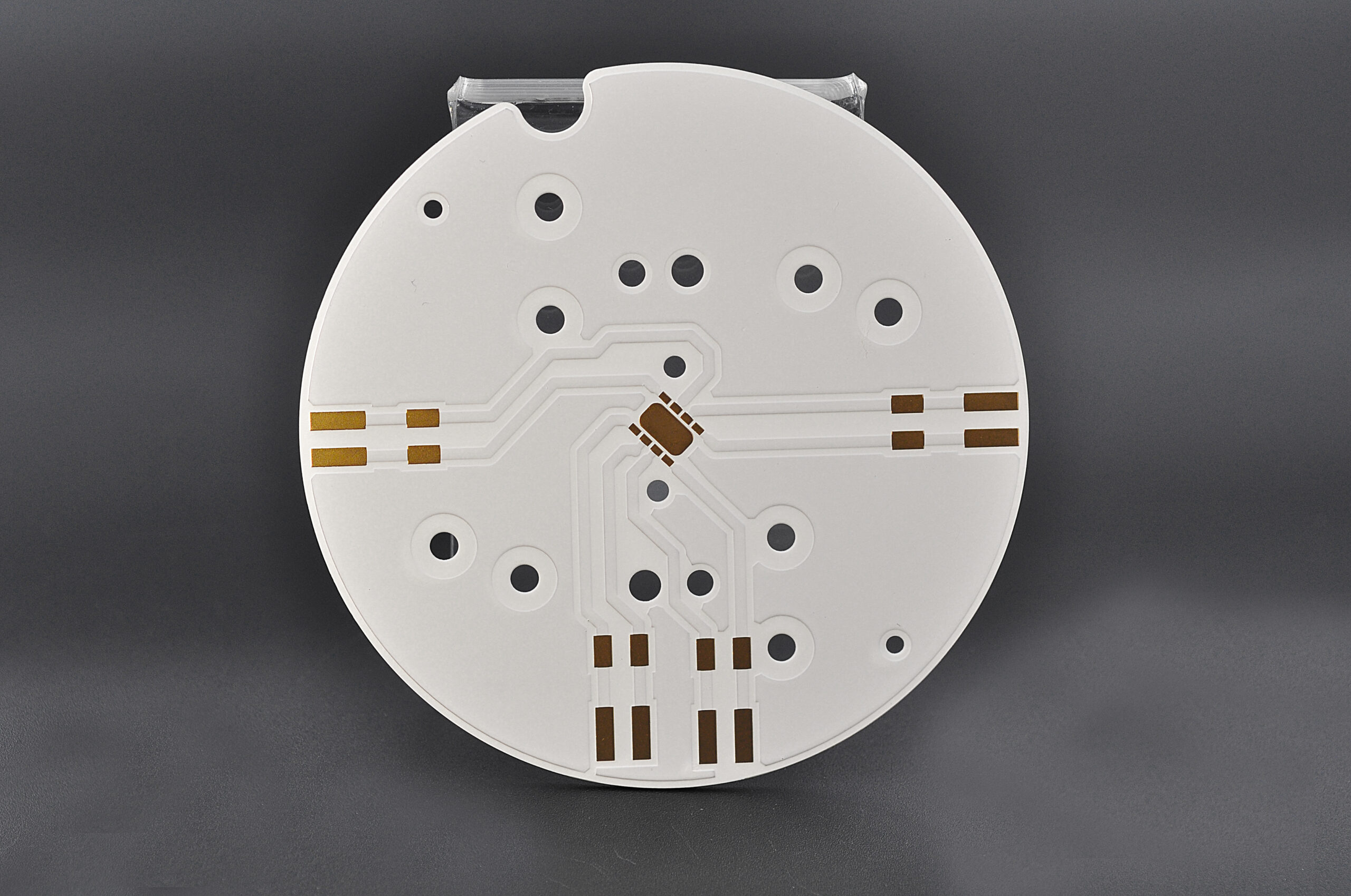
The Structures of a LED PCB Board in Manufacturing?
A LED PCB is similar to traditional rigid board, the only one difference is the LED mounting on the pads. Herein, we listing the basic composition of a LED pcb board, let’s see it together.
1. Substrate – The base of the PCB, which can be flexible (like polyimide), metal alloy (aluminum, copper), or ceramic, depending on the required thermal performance.
2. Copper foil – A thin layer of copper is used for forming the circuit paths on the PCB.
3. Solder mask – This is a protective layer covers the copper paths to prevent oxidation and short circuits. It also aids in SMT (surface mounted technology) soldering.
4. Silkscreen – Used to print labels, logos, vendors, symbols, and pick and place on the PCB for easy identification during assembly.
5. Adhesives – Aiming to bond different PCB layers, different material used different adhesive, always are prepreg (PP).
6. LEDs: The main components mounted on the PCB, available in various sizes, colors, power ratings, voltages and so on.
Your Reliable LED PCB Board Manufacturer – EBest Circuit (Best Technology)
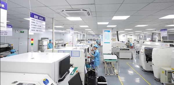
EBest Circuit (Best Technology) stands out as a leading manufacturer of high-quality LED PCB boards. We offer a wide range of products and services to cater to various needs. With extensive experience and expertise in the industry, we are committed to providing reliable and cost-effective solutions.
Advanced Facilities
We are equipped with advanced machinery and technology, ensuring precision and efficiency in production.
Experienced Team
Our skilled professionals are dedicated to delivering topnotch LED printed circuit boards. Most of our core members has more than 10 years-experience in the PCB manufacturing.
Quality Assurance
We have passed ISO9001, ISO13485, IATF16949 certifications, and integrated them into our daily manufacturing process. These strict quality control measures can make sure every product meets the highest standards of industry.
Customization
We offer tailored customized LED PCB board solutions to meet customer specific requirements.
Competitive Pricing
EBest Circuit (Best Technology) has our own factory in China and Vietnam, we can provide most affordable solutions without compromising on quality.
Choosing EBest Circuit (Best Technology) means opting for excellence, reliability, and superior service. Partner with us for your LED PCB needs and experience the difference we bring.
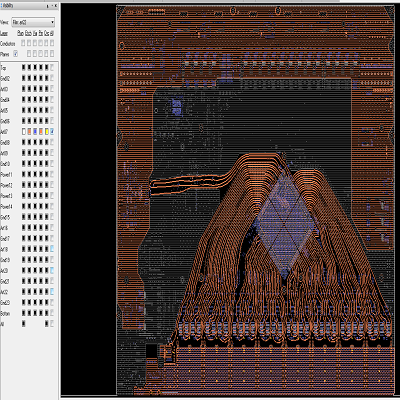
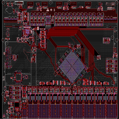
When designing high-speed PCBs, several critical factors must be considered to ensure optimal performance. These include signal integrity, impedance control, and minimizing electromagnetic interference (EMI). Below is an ultra high speed camera PCB solution made by EBest Circuit (Best Technology):
An ultra-high-speed camera rigid-flex circuit board
[1]: XCKU060 chip
[2]: 20A maximum current
[3]: Four DDR4 channels
[4]: 20 layers PCB
Camera PCB design considerations:
1. When the Camera adopts a connector: when the MIPI differential signal passes through the connector, the adjacent differential signal pairs must be isolated using GND pins; If it is not convenient to punch holes, the spacing between the difference pairs is at least 15mil.
2. If there is a reserved test point for the Camera connection seat, it should be close to the connection seat, and the Stub on the cable should be as short as possible.
3. Decoupling capacitors of AVDD/DOVDD/DVDD power supply need to be placed as close as possible to the Camera connection base.
4. The Camera layout needs to be far away from high-power radiation devices, such as GSM antennas.
5. CIF/MIPI and other signals, if there is a board to board connection through the connector, it is recommended that all signals be connected with a certain resistance value (between 2.2ohm and 10ohm, depending on the SI test), and reserve TVS devices.
EBest Circuit (Best Technology) offers one-stop solutions for our values customers. And we provide free technical support for our customers. If you have similiar requirements, welcome to contact us at any time!
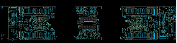
A high-speed circuit handles signals that switch quickly or operate at high frequencies, typically above 50 MHz, though some advanced systems may go into the GHz range. EBest Circuit (Best Technology) is a one-stop PCB manufacturer that covers pcb design, pcb layout, pcb diagram, DFM, SI, PI analysis, PCB manufacturing and so on. In the following, you can see a high speed pcb design solution for industrial switch that we cooperated with our customer.
32 x 400GE industrial switch
[1]: Marvell-400G chip
[2]: 200A maximum current
[3]: Single pair differential line 56G optical network
[4]: 24 layers high power PCB
What’s the Best Material for High-Speed PCB Design?
Choosing the right material is vital for maintaining signal integrity and achieving optimal performance. The material impacts the board’s dielectric constant (Dk), loss tangent, and overall signal quality. Common materials include:
FR4: Widely used but not ideal for very high frequencies due to higher loss tangent.
Rogers (RO4000 series): Preferred for high-speed designs thanks to its low dielectric constant and loss tangent.
Teflon: Excellent for high-frequency applications but more expensive and harder to process.
Selecting the appropriate material ensures the PCB can handle high-speed signals without compromising performance.
For the PCB design service, we can make sure the one-time success to save much time and money for customers. Our goal is to work with customers together and win more market with our clients. Just feel free to contact our technical team if you have similiar designs.
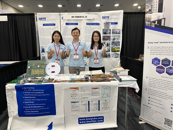
EBest Circuit (Best Technology), a China-based PCB & PCBA manufacturer will be exhibiting at New-Tech 2024 in EXPO Tel-Aviv, Israel at booth No. 66 from May 28, 2024 to May 29, 2024(Western Time). Actually, we have participated in such exhibition for several years. At our exhibition booth, attendees will be able to learn more about our company for PCB manufacturing and PCB assembly technology. Here are some pictures for your reference.
For interested professionals, EBest Circuit (Best Technology) had on hand experts to offer detailed insights and experience on PCB assembly, covering PCB prototype and low/high-volume production. For more information on PCB assembly and fabrication, welcome to visit our booth.
You will see 10mm to 1,500 mm flexible circuit board, from 2layer rigid-flex circuit to 50 layers, 1/2 OZ copper to 3 OZ, 0.15mm extra thin FR4 PCB to 30 OZ heavy copper, various ceramic PCBs (thick film, thin film, DPC, DBC, HTCC, AMB, LTCC). Our new products also will be shown in this exhibition, like copper/aluminum busbar PCB, transparent/PI/rubber silicone flexible heating film, semi-flexible PCB, semi-flexible aluminum PCB.
In EBest Circuit (Best Technology), you will enjoy one-stop service from components sourcing, board fabrication (FPC, PCB, MCPCB, Ceramic PCB) and final assembly with programming and testing and metal dome that is used in conjunction with a printed circuit board, flex circuit, or membrane switch, become normally-open tactile switches. we have four types of metal domes: four legs with size from 5mm-20mm; triangle with size 4mm-12mm; round dome with size 4-16mm, oblong dome with size 3.7mm-58.1mm, and we also make dome with adhesive, named dome array, custom membrane switches also available in Best Tech.
You are warmly welcome to see how we can manage the components wastage and efficiency to help save your time, money and energy.
About New-Tech:
The New-Tech Exhibition is the largest and major exhibition of the Hi–Tech & Electronics in Israel. More than 150 companies, who lead these fields in Israel and around the world, will take part and exhibit in this trade show.
This exhibition shows a comprehensive array of electronic components, production processes, subcontracting services, clean room equipment, electro-optic devices, test equipment, printed circuit boards, industrial materials, computerization solutions, robotics, power systems, RF/microwave technologies, and more. Attendees can explore cutting-edge innovations in development, design, engineering, and procurement across various industries.
It is important to note:
1. Participation in the exhibition is conditional on prior registration, even for invited customers.
2. After registration and before the conference, a code will be sent to the mobile to confirm participation in the conference.