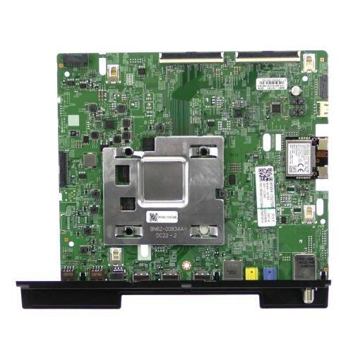
PCB manufacturing PCB manufacturing
Home > Blog

Custom UHDI PCB Manufacturer | Quick Prototype Fabrication

April 2nd, 2026

UHDI PCB​ represents the pinnacle of high-density interconnect technology, enabling the advanced miniaturization and superior performance required by next-generation electronics. This comprehensive guide delves into everything you need to know about UHDI PCBs, from their fundamental definition and materials to design considerations and how to select the right manufacturing partner for your prototype and production needs.

What are the core pain points when sourcing UHDI PCBs?

  • Finding True Expertise:​ Many manufacturers claim HDI capability, but few possess the specialized equipment and process control for genuine UHDI features like 25µm line/space and microvias below 50µm.
  • Prototype Delays:​ Critical R&D and testing phases are stalled by long lead times for complex UHDI prototypes, delaying time-to-market for cutting-edge products.
  • Unpredictable Costs:​ Opaque pricing structures and unexpected engineering charges for impedance control and advanced materials like Megtron 6 or Rogers make budgeting difficult.
  • Design for Manufacturing (DFM) Gaps:​ A lack of proactive engineering support leads to design revisions, respins, and failures because the board wasn’t optimized for UHDI fabrication processes.
  • Fragmented Supply Chain:​ Managing separate vendors for design, PCB fabrication, assembly, and testing adds complexity, risk, and communication overhead.

Best Technology provides integrated solutions to these exact challenges.​ As a specialized UHDI PCB manufacturer, we bridge the gap between ambitious design and reliable, high-yield manufacturing.
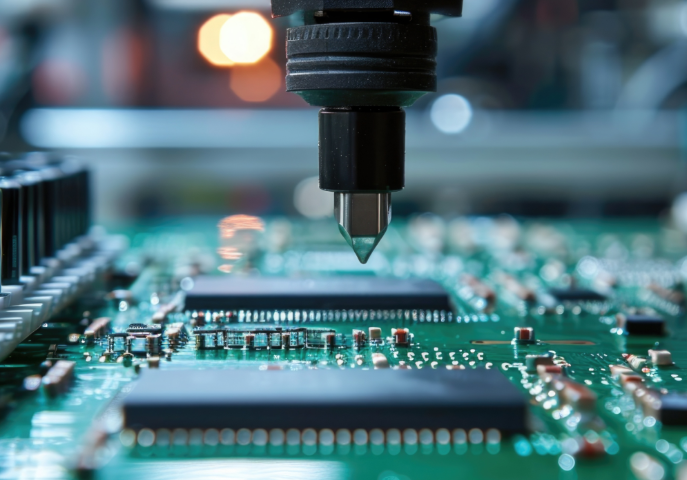
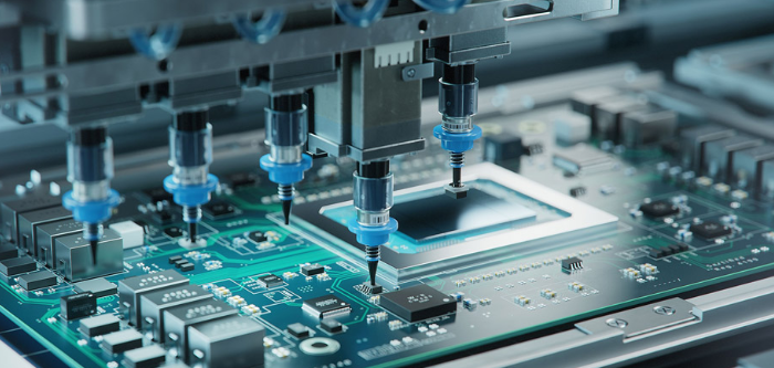
  • Proven UHDI Process Mastery:​ Our investment in technology like laser direct imaging and advanced laser drilling allows us to reliably produce 2/2 mil lines and 0.1mm microvias, meeting the stringent demands of UHDI circuits.
  • Rapid Prototype Service:​ We prioritize quick-turn UHDI PCB prototype fabrication, with expedited services available to get your boards in hand for testing in as little as 48-72 hours for multilayer builds, accelerating your development cycle.
  • Transparent and Competitive Pricing:​ We offer clear, upfront quotations for prototype and volume production, with cost breakdowns for different quantities (e.g., 1 pc, 100 pcs, 1000 pcs) and materials, ensuring no surprises.
  • Expert DFM and Stack-up Support:​ Our engineering team works with you from the start, providing preliminary stack-up structures and impedance modeling guidance (e.g., for 80 GHz applications) to ensure your design is manufacturable and performs as intended.
  • Full Turnkey Service:​ From UHDI printed circuit board fabrication and component sourcing to precise assembly and rigorous testing, we offer a one-stop solution, simplifying your supply chain and ensuring accountability.

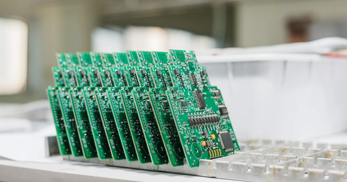
EBest Circuit (Best Technology) is a premier and experienced UHDI PCB manufacturer in China. With 20 years of dedicated PCB fabrication expertise, we have evolved into a trusted full-turnkey solution provider. We specialize in advanced technologies including UHDI, RF/microwave PCBs (using Rogers, Taconic, Megtron materials), heavy copper, and rigid-flex boards. Our commitment is underscored by ISO9001, IATF16949, and ISO13485 certifications, and a 97% on-time delivery rate. We combine state-of-the-art equipment with deep engineering knowledge to deliver high-quality, high-precision PCBs for the most demanding applications. For your UHDI project, pls feel free to contact our experts at sales@bestpcbs.com.
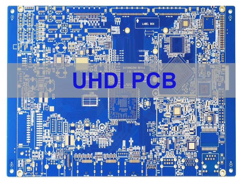
What Is a UHDI PCB?

A UHDI (Ultra High-Density Interconnect) PCB is an advanced type of printed circuit board characterized by exceptionally fine features, which enable a dramatically higher wiring density within a given area compared to standard HDI or traditional PCBs. This is achieved through extremely narrow trace widths/spacing, smaller microvias, and higher interconnect pad density.

Key characteristics defining a UHDI circuit board include:
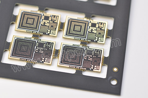
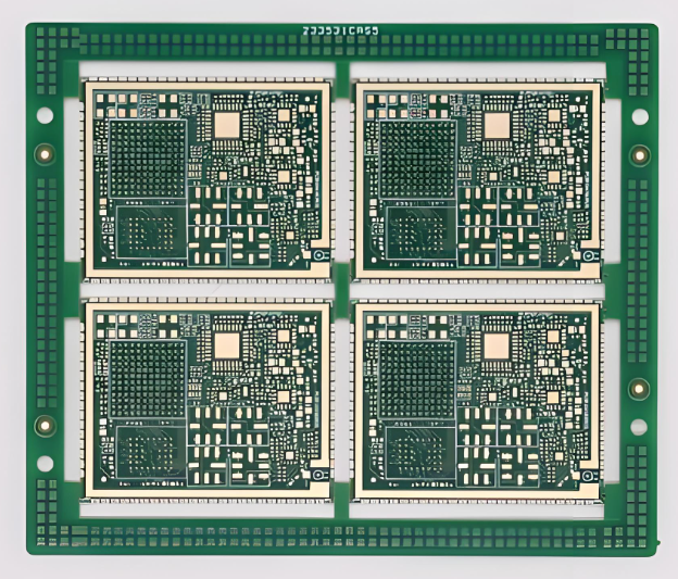
  • Extremely Fine Lines/Spaces:​ Feature sizes of 30µm (1.2 mil) and below, pushing towards 25µm (1 mil) or less. Our capabilities support advanced HDI features down to 2/2 mil.
  • Microvias:​ Extensive use of laser-drilled microvias with diameters below 75µm (3 mil), often in stacked or staggered configurations. Our equipment allows for minimum laser-drilled via diameters of 4 mil (0.1mm).
  • High Layer Count:​ Often involves 10+ layers to accommodate complex routing in compact spaces. We can manufacture up to 32-layer multilayer boards.
  • Advanced Materials:​ Frequent use of high-performance, low-loss laminate materials to ensure signal integrity at high speeds.
  • Any-Layer Interconnection:​ The most advanced form where microvias can connect any two layers in the stack-up, maximizing routing freedom.

In essence, a UHDI printed circuit board (PCB) is the enabling hardware for today’s most compact and high-performance electronic devices, such as advanced smartphones, wearable technology, and high-speed computing modules, where real estate is at a premium and signal speeds are critical.

What Is the Difference Between a UHDI PCB and an HDI PCB?

While both HDI (High-Density Interconnect) and UHDI PCBs aim to increase wiring density, UHDI represents a significant evolution and a higher tier of capability. Think of HDI as the foundation and UHDI as the specialized, cutting-edge extension of that technology.

The primary differences are quantitative and qualitative advances in manufacturing tolerances and design rules:

FeatureHDI PCBUHDI PCB
Line/Space (Typical)3/3 mil (75/75 µm) and above2/2 mil (50/50 µm) and below, targeting ≤1/1 mil
Microvia Diameter≥4 mil (100 µm)≤3 mil (75 µm), targeting 1-2 mil
Pad SizeRelatively largerExtremely small, often at the limit of registration accuracy
Interconnect DensityHighUltra-High
Primary DriverSpace saving, moderate performanceMaximum miniaturization, highest signal integrity for high-speed/frequency
Manufacturing ProcessAdvanced laser drilling, sequential laminationSame as HDI, but with tighter process control, more advanced imaging (e.g., LDI), and often more lamination cycles.

In summary, all UHDI PCBs are HDI, but not all HDI PCBs qualify as UHDI. UHDI pushes the boundaries of HDI technology to its extremes, requiring more precise and controlled manufacturing processes. For instance, our standard HDI capability offers 3/3 mil lines, while our advanced processes support the 2/2 mil features that edge into UHDI territory, demonstrating the technical progression.

What Is the Difference Between a UHDI PCB and an RF PCB?

This is a crucial distinction: UHDI and RF PCB are classifications based on different primary objectives. One focuses on density, the other on signal performance​ at high frequencies. They are not mutually exclusive and often converge in advanced applications.

AspectUHDI PCBRF PCB
Primary GoalMaximize density & miniaturization.Signal integrity at high frequency.
Key MetricFine features (line/space, via density).Material properties (Dk/Df).
Critical MaterialsAdvanced FR4, thin cores.Specialized low-loss laminates (e.g., Rogers, Megtron).
Design FocusRouting complexity & microvias.Transmission line geometry & grounding.
Typical ApplicationsMobile, wearable, compact devices.5G/6G, radar, satellite comms.

The convergence of these two technologies results in what is known as an RF UHDI PCB. The most advanced boards, like the one mentioned in the customer inquiry for 80 GHz operation, must be both. They require the ultra-fine features of UHDI to route high-density, high-pin-count RF components and​ the specialized materials (like Megtron 6 or Rogers) of an RF PCB to maintain signal integrity at such extreme frequencies. Manufacturing such a board requires a vendor proficient in both domains—handling advanced materials with precise impedance control while executing UHDI-level fine features and microvia structures.

What Material Is a UHDI PCB Made Of?

The materials for a UHDI PCB are selected to support both the fine-feature fabrication processes and the intended electrical performance, often high-speed or high-frequency.

Core Material Systems:

  1. Standard & High-Performance FR4:For UHDI applications not at the extreme high-frequency edge, high-Tg FR4 (Tg ≥ 170°C) like KB6167 or IT180 is common. It offers good stability for sequential lamination cycles. Our material inventory includes high-Tg, no-halogen FR4 options suitable for complex multilayers.
  2. Low-Loss / High-Speed Laminates:For UHDI boards where signal integrity is paramount, materials with a lower dissipation factor (Df) are mandatory. This includes:
    • Megtron 6/7/8 (Panasonic):​ A popular choice for high-speed digital and RF applications, offering excellent electrical properties.
    • Rogers RO4000® Series:​ Ceramic-filled hydrocarbon laminates ideal for RF and microwave designs.
    • Isola FR408HR, Nelco N4000-13:​ Other high-performance options for demanding electrical environments.
  3. Thin Dielectric Laminates and Prepregs: UHDI relies on very thin core and prepreg layers (e.g., 1080, 106, 1035 styles) to achieve the close layer spacing needed for microvias and controlled impedance in dense layouts. We utilize a wide range of PP types, including 1080 (0.07mm), 2116 (0.11mm), and 7628 (0.175mm).
  4. Advanced Copper Foils:Treated or very low-profile copper foils are used to improve adhesion and etching yields for extremely fine traces.

The choice of material is dictated by the application’s frequency, data rate, thermal, and reliability requirements.​ For the 80 GHz application specified in the inquiry, Megtron 6 or Rogers​ would be the recommended substrate materials to meet the low-loss demands at that frequency, fabricated using UHDI processes.

How to Design the Preliminary Stack-Up Structure of a UHDI Printed Circuit Board?

Designing the stack-up is a foundational step in UHDI PCB development, critical for impedance control, signal integrity, power integrity, and manufacturability. A well-planned stack-up saves multiple prototyping cycles.

A step-by-step approach for a preliminary UHDI PCB stack-up design:

  • Define Requirements:​ Start with the board’s functional needs: number of signal layers, power/ground planes, target impedance (e.g., 50Ω single-ended, 100Ω differential), operating frequency (e.g., 80 GHz), and board thickness constraints.
  • Select Core Material:​ Based on frequency/speed, choose the dielectric material (e.g., Megtron 6 for RF, High-Tg FR4 for high-density digital). Obtain its certified Dk and Df values at your target frequency from the manufacturer’s datasheet.
  • Determine Dielectric Thickness:​ This is the distance between adjacent copper layers. For UHDI, these are often very thin (e.g., 2-4 mils) to enable microvias and tight coupling. Use an impedance calculator (like Polar Si9000) with the material Dk, target impedance, and desired trace width to solve for the required dielectric thickness.
  • Choose Copper Weight:​ Thinner copper (e.g., ½ oz or 1/3 oz) is preferred for etching fine traces. Standard UHDI designs often use ½ oz (17.5 µm) finished copper for signal layers. Heavier copper (1 oz+) may be used for power planes.
  • Arrange Layer Sequence:​ Follow a symmetrical stack-up to prevent warpage. Use a signal-ground-signal (S-G-S) sandwich for critical high-speed lines to provide a clear return path. Place power and ground planes adjacent to each other to form a decoupling capacitor.
  • Plan the Via Strategy:​ Decide on via types: through-hole vias, blind vias (from surface to inner layer), buried vias (between inner layers), and microvias (typically <6 mil diameter). In UHDI, microvias are key. Plan their depth (1-n layers) and whether they will be stacked or staggered.
  • Consult Your Manufacturer Early:​ Engage with your UHDI PCB manufacturer (like Best Technology) during this phase. Share your target stack-up for a DFM review. We can provide feedback on material availability, feasible dielectric thicknesses, and recommend adjustments for optimal yield and performance.

Example Preliminary Stack-Up for a 12-Layer UHDI/RF Board:

LayerTypeMaterial/ThicknessDescription
L1Signal½ oz CuTop Layer, RF Components
Dielectric3.5 mil Megtron 6
L2Ground1 oz CuSolid Ground Plane
Dielectric4 mil Prepreg
L3Signal½ oz CuHigh-Speed Signals
Core4 mil Megt6 Core
L4Power1 oz CuPower Plane 1
L12Signal½ oz CuBottom Layer

This is a simplified example. The actual design would be built in collaboration with our engineers.

Where Is a UHDI PCB Used?

UHDI PCBs are indispensable in industries where miniaturization, high performance, and reliability are non-negotiable. Their ability to pack immense functionality into a tiny footprint makes them the backbone of modern advanced electronics.

Primary application areas for UHDI printed circuit boards include:

  • Consumer Electronics:​ Smartphones, tablets, laptops, and wearables (smartwatches, AR/VR headsets) constantly push for smaller, lighter, and more powerful devices.
  • Medical Electronics:​ Implantable devices (pacemakers, neurostimulators), advanced diagnostic imaging equipment, and miniature surgical tools.
  • Telecommunications & 5G/6G Infrastructure:​ RF front-end modules, millimeter-wave antennas, base station processing units, and network switches operating at extremely high frequencies.
  • Automotive Electronics:​ Advanced Driver-Assistance Systems (ADAS), LiDAR sensors, infotainment systems, and vehicle control units in electric and autonomous vehicles.
  • Aerospace and Defense:​ Avionics, satellite communication systems, radar, and guidance systems where reliability and performance in harsh environments are critical.
  • High-Performance Computing (HPC):​ Servers, data centers, and AI accelerator modules that require high-speed data transfer between densely packed components.

In each case, the UHDI circuit board enables a critical size reduction or performance enhancement that would be impossible with conventional PCB technology.

Top 10 UHDI Circuit Board Manufacturers in China

Identifying the “top” manufacturers depends heavily on specific project needs—prototype vs. volume, technology focus (e.g., RF UHDI), and industry vertical. Rather than a simple list, here are key criteria for evaluation and how Best Technology positions itself:

Key Evaluation Criteria for a UHDI PCB Manufacturer:

  • Technology Certification:​ Demonstrated capability in ≤ 3/3 mil line/space, microvia drilling ≤ 4 mil, and any-layer HDI processes. We support 2/2 mil lines and 4 mil (0.1mm) laser-drilled microvias.
  • Material Expertise:​ Proven experience with high-frequency laminates (Rogers, Taconic, Megtron) and high-Tg materials. Our material portfolio includes these advanced substrates.
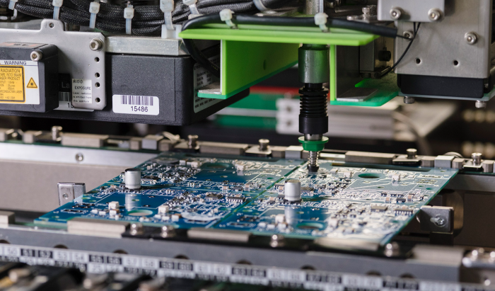
  • Advanced Equipment:​ Investment in LDI (Laser Direct Imaging) for fine-line patterning, high-precision laser drills, and AOI (Automatic Optical Inspection). We utilize equipment from global leaders like Hitachi (drilling) and Israeli AOI systems.
  • Engineering Support:​ Strong DFM and stack-up design support team. Our engineers provide preliminary stack-up structures for impedance matching.
  • Quality Systems:​ Certifications like IATF 16949 (automotive) and ISO 13485 (medical) indicate process rigor. We hold these certifications, among others.
  • Prototype Speed:​ Willingness and ability to offer quick-turn prototype services. We provide expedited 24-72 hour turns for multilayer prototypes.
  • Volume Scalability:​ Capacity to scale from prototype to medium/high-volume production seamlessly. Our monthly capacity is over 28,900 square meters.
  • Testing Capability:​ In-house electrical testing, impedance testing, and reliability testing. We employ flying probe testers, universal E-testers, and micro-section analysis.
  • Vertical Integration:​ Offering turnkey services (PCB + Assembly) reduces supply chain risk. We are a full turnkey provider.
  • Customer Service & Communication:​ Responsive, technical sales and project management. We pride ourselves on one-on-one engineering support and fast response times.

Top 10 UHDI Circuit Board Manufacturers in China (Reference Table)

CompanyProcess CapabilityPrototype Lead Time
EBest Circuit (Best Technology)1+N+1 to 3+N+3; PTH ≤0.1mm24 hours
PCBWayMicrovias; 0.10mm laser hole; 55/55μm L/S24 hours
PCBCartHDI; 2.5 mil trace/space2 days to 5 weeks
JLCPCBBlind/buried vias; 0.15mm via hole24–72 hours
OurPCB2.5 mil trace/space; 0.1mm microvia24 hours to 7 days
RayPCB3 mil trace/space; ~150μm via1–5 days
KKPCB2/2 mil L/S; 0.075–0.15mm laser drillTo be confirmed
WellPCB1.8 mil spacing; microvia supportAbout 2 weeks
Weller PCB2/2 mil HDI; microvias <150μm1–2 days
PCBBUY2/2 mil HDI; ≥0.075mm blind via24 hours to 7 days

Note: The ranking above is for reference only. The right UHDI PCB manufacturer should be selected based on your required line/space, microvia structure, material system, stack-up complexity, prototype speed, and volume production needs.

Why Choose EBest Circuit (Best Technology) for UHDI PCB Prototype Fabrication?

Selecting the right partner for your UHDI prototype is critical to project success. Best Technology is engineered to be that partner, offering a unique blend of advanced capability and responsive service.

  • Proven Advanced Technology Foundation:​ Our core manufacturing capabilities are tailored for complexity. We routinely handle ultra-fine features (3/3 mil standard, 2/2 mil advanced HDI), high layer counts (up to 32 layers), and controlled impedance (tolerance ±10% for >50Ω, ±5Ω for ≤50Ω). Our expertise in heavy copper (up to 20 oz) and various substrates (FR4, MCPCB, Ceramic) translates to robust process control for delicate UHDI structures.
  • Dedicated Quick-Turn Prototype Service:​ We understand the urgency of innovation. For standard-specification FR4 prototypes under 1 sq meter, we offer rapid turnaround (e.g., 10 days for 6-layer, 72 hours for expedited service). This service extends to complex builds, allowing you to iterate and validate designs quickly, compressing your R&D timeline.
  • Comprehensive Quality and Reliability Assurance:​ Quality is integrated into our process. We hold ISO 9001:2015, IATF 16949:2016, and ISO 13485:2016 certifications. Our inspection regime includes Automated Optical Inspection (AOI) from industry leaders, X-ray copper thickness testers, flying probe testing, and micro-section analysis to validate every microvia and trace.
  • Expert Engineering Partnership:​ We don’t just manufacture; we collaborate. Our engineering team provides proactive DFM feedback, assists with material selection (crucial for 80 GHz RF UHDI boards), and delivers preliminary stack-up structures for your impedance modeling. We help bridge the gap between your design and a manufacturable, high-performance product.
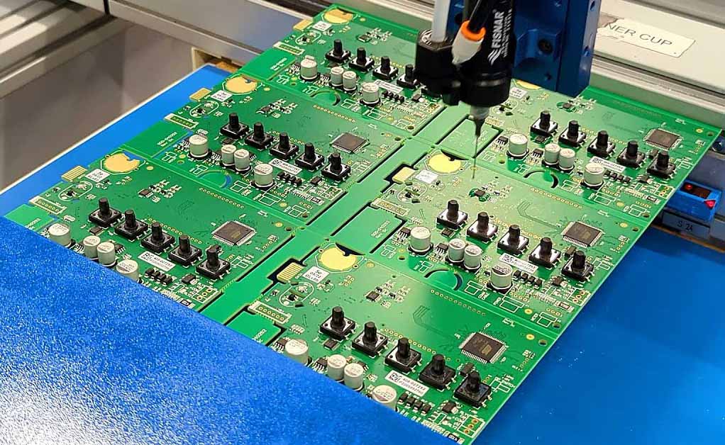
  • Full Turnkey Solution and Support:​ From the initial UHDI PCB prototype quote to final box build, we provide a seamless, accountable journey. Our one-stop service covers PCB fabrication, component sourcing, PCB assembly (with capabilities for 01005 components and 0.25mm BGA pitch), and testing. You get a single point of contact, simplified logistics, and faster overall project completion.

How to Request a Quote for UHDI PCB Prototype Fabrication?

Requesting a quote for a UHDI PCB is straightforward when you provide the right information. A complete and clear request ensures an accurate, fast, and competitive quotation. Here is a step-by-step guide based on common requirements, like those from the Technion inquiry:

  1. Prepare Your Design Files:​ The essential package includes your Gerber files (RS-274X format preferred), drill files, and a completed PCB fabrication drawing​ with all critical dimensions, tolerances, and notes.
  2. Specify Technical Requirements:Create a separate document detailing:
    • Layer Count & Stack-up:​ Preferred materials (e.g., “Megtron 6 for all layers” or “Rogers 4350B for L1-L4”).
    • Finished Board Thickness & Tolerance.
    • Copper Weight:​ For inner and outer layers (e.g., ½ oz inner, 1 oz outer).
    • Surface Finish:​ Specify one, e.g., ENIG, ENEPIG, Immersion Silver, Hard Gold (for edge connectors).
    • Impedance Control:​ Target values, tolerance (e.g., 50Ω ±10%), and which layers/differentials are controlled.
    • Special Requirements:​ Any specific needs like filled/via-in-pad, edge plating, or tight impedance tolerances for RF sections.
  3. Define Quantity and Urgency:
    • Clearly state the quantities you need quotes for: Prototype quantity (e.g., 5 pcs), 100 units, and 1000 units.​ This allows us to show volume pricing breaks.
    • Indicate your required lead time​ (e.g., “Standard” or “Expedited”).
  4. Request a Preliminary Stack-Up (if needed): If you are in the early design phase (like the 80 GHz application mentioned), you can request that we provide a preliminary stack-up structure​ based on your material choice and impedance targets. This allows you to perform accurate impedance modeling in your design tools.
  5. Submit and Engage: Send your complete package to sales@bestpcbs.com. A dedicated engineering sales person will review your files, may ask clarifying questions, and will provide a formal quotation typically within 24 hours, including unit price, volume pricing, and lead time options.

In closing, UHDI PCBs​ are the critical hardware foundation enabling the relentless march of electronic miniaturization and performance enhancement across industries from healthcare to telecommunications. This article has explored the what, why, and how of UHDI technology, the key differences from HDI and RF PCBs, and the practical steps involved in designing and procuring these advanced boards.

EBest Circuit (Best Technology)​ stands as a reliable specialist in this field. With two decades of experience, certified quality systems, advanced manufacturing capabilities supporting fine features and advanced materials, and a commitment to fast-turn prototypes and full turnkey solutions, we are equipped to bring your most challenging UHDI circuit board designs to life. Pls feel free to contact our technical sales team anytime at sales@bestpcbs.com​ for a comprehensive consultation and quotation.

FAQs About UHDI PCBs

1. What is the minimum line/space Best Technology can achieve for UHDI prototypes?

We regularly manufacture advanced HDI boards with 3/3 mil (75/75 µm) line/space. For designs pushing into UHDI territory, we have the capability to support 2/2 mil (50/50 µm) features, subject to a full DFM review of your specific design.

2. Can you handle the RF materials like Rogers or Megtron 6 required for high-frequency UHDI boards?

Yes, absolutely. We have extensive experience processing high-frequency, low-loss laminates including the Rogers series (e.g., RO4003C, RO4350B), Taconic, and Panasonic’s Megtron 6/7. We can guide you on material selection for applications like 80 GHz and ensure proper lamination and impedance control.

3. What is the typical lead time for a 10-layer UHDI PCB prototype?

For a standard 10-layer FR4 prototype (<1 sq. meter), our typical lead time is 12 business days. We offer expedited services that can significantly reduce this time. The lead time for a UHDI board with advanced materials (like Megtron 6) and features will be confirmed upon review of your specific technical files.

4. Do you provide impedance control and testing reports?

Yes. We have in-house impedance modeling expertise and can control impedance to tight tolerances (e.g., ±10% for values >50Ω, ±5Ω for ≤50Ω). We can provide impedance test coupons on the panel and, upon request, supply test reports to verify performance.

5. Do you offer turnkey services including component sourcing and assembly for UHDI PCBA?

Yes, we are a full turnkey provider. We can manage the entire process: manufacturing the UHDI printed circuit board, sourcing all components from authorized distributors, performing precise SMT assembly (handling 01005 components and 0.25mm BGA pitch), and conducting full functional testing. This simplifies your supply chain and ensures accountability.

Rigorous Quality RF HDI Circuit Board Manufacturer from Prototypes to Assembly

March 31st, 2026

RF HDI circuit board is the critical foundation for high-frequency, high-speed electronics, merging the signal integrity of radio frequency designs with the dense interconnects of HDI technology. This article provides a comprehensive guide to RF HDI boards, addressing key design challenges and showcasing how a manufacturer with full turnkey capabilities ensures success from prototype to final assembly.

Engineers and procurement specialists often face significant hurdles when sourcing advanced RF HDI circuit boards. Common pain points include:

  • Struggling to find a manufacturer capable of handling ultra-fine features like 3.3-mil flip-chip pitch.
  • Experiencing inconsistent quality or outright rejection from suppliers lacking advanced HDI processes.
  • Facing long lead times and poor communication, especially with offshore suppliers that can’t support rapid iteration.
  • Dealing with the complexity of managing separate vendors for RF PCB fabrication and assembly.
  • Receiving inadequate DFM feedback, resulting in designs that are difficult or costly to manufacture.

At EBest Circuit (Best Technology), we resolve these challenges through our integrated, expert-driven approach. Our solutions are built on:

  • Proven Advanced Process Capability:​ Expertise in HDI PCB manufacturing​ with 3/3 mil line/space and 4 mil laser micro-drilling.
  • Full In-House Control:​ A true one-stop service encompassing design, advanced packaging substrate manufacturing, fabrication, and assembly under rigorous quality systems.
  • Rapid and Reliable Execution:​ Dedicated engineering support and a 24-hour rapid prototyping service to accelerate your development cycle.
  • Turnkey Simplification:​ A seamless supply chain from component sourcing to final box build, managed by a single point of contact.
  • Collaborative Engineering Partnership:​ Proactive Design for Manufacturability (DFM)​ analysis to optimize your fine-pitch flip-chip assembly​ and RF performance before production begins.

Founded in 2006, EBest Circuit (Best Technology) is a certified, full-service PCB and PCBA manufacturer with two decades of specialization in high-technology circuit boards. We operate a 28,900 sq. meter facility equipped with state-of-the-art machinery, from CNC laser drills for high-density via PCB​ creation to advanced SMT lines for precision assembly. Holding certifications like ISO 9001:2015, IATF 16949, and ISO 13485:2016, we serve over 1,700 clients across 40+ countries with a 97% on-time delivery rate. Our core strength lies in transforming complex RF and HDI designs into reliable, high-performance products. For a consultation on your next project, pls feel free to contact us at sales@bestpcbs.com.

RF HDI Circuit Board

What Is An RF HDI Circuit Board?

An RF HDI circuit board is a sophisticated printed circuit board designed to operate at high frequencies (typically from hundreds of MHz to several GHz) while incorporating High-Density Interconnect (HDI) technology. It combines the need for controlled impedance, low signal loss, and minimal electromagnetic interference of RF design with the space-saving, high-performance interconnects of HDI, which uses micro-vias, fine lines, and multiple via-in-pad structures. This convergence is essential for modern compact, high-speed devices like 5G infrastructure, advanced radar systems, and high-frequency test equipment.

Key characteristics include:

  • Advanced Materials:​ Use of low-loss, stable dielectric substrates like Rogers RO4350B or Taconic, rather than standard FR4.
  • Micro-Via Technology:​ Extensive use of blind, buried, and stacked micro-vias (as small as 4 mils in diameter) to facilitate dense routing.
  • Fine Features:​ Trace/space widths down to 3/3 mils to accommodate fine-pitch ICs and complex routing.
  • Impedance Control:​ Tightly controlled dielectric thickness and trace geometry to maintain specific impedance values (e.g., 50Ω, 100Ω differential).
  • Thermal Management:​ Strategic placement of thermal vias and use of materials with appropriate thermal conductivity to dissipate heat from active components.

In summary, an RF HDI board is the enabling platform for electronics where signal speed, integrity, and component density are all paramount, requiring a manufacturer with precise process control and material expertise.

RF HDI Circuit Board

What Is the Difference Between RF and HDI Circuit Boards?

While both RF and HDI PCBs represent advanced circuit board technologies, they prioritize different design and performance goals. Understanding their distinctions is crucial for selecting the right board for your application and the right manufacturer for your project.

FeatureRF Circuit BoardHDI Circuit BoardRF HDI Circuit Board
Primary FocusHigh-frequency signal performanceHigh wiring densityHigh-frequency performance + high density
Typical MaterialLow-loss laminatesFR4 / high-performance FR4Low-loss laminates
Main ChallengeImpedance and dielectric loss controlMicrovia and fine-line reliabilityImpedance control + microvia reliability
Common FeaturesControlled impedance, ground isolationBlind/buried vias, via-in-padFine-pitch layout, via-in-pad
Process FocusMaterial consistencyLaser drilling, sequential laminationCombined RF + HDI process control

RF Boards​ focus on the “quality” of the signal path, minimizing loss and distortion. HDI Boards​ focus on the “quantity” and efficiency of connections, packing more functionality into less space. An RF HDI Board, the subject of this article, demands expertise in both domains, making the choice of manufacturer—one like EBest Circuit with proven capability in both RF PCB manufacturing​ and HDI PCB manufacturing—critical to success.

How Many Ground Vias Can Fit Under a Component?

Maximizing ground vias under a component, especially an RF die or a BGA, is vital for providing a low-inductance path to ground, improving thermal dissipation, and shielding. The quantity is determined by a combination of your design rules and the manufacturer’s fabrication limits.

The number is primarily constrained by:

  • Via Diameter and Pitch:​ Our standard micro-drilling capabilities​ allow for laser-drilled micro-vias as small as 4 mils (0.1mm) in diameter. The minimum via-to-via spacing (pitch) is typically 8-10 mils for these micro-vias. A smaller diameter and tighter pitch allow for more vias.
  • Pad Size:​ The component pad size sets the available real estate. Using a via-in-pad design is most effective.
  • Aspect Ratio:​ For thicker boards, the aspect ratio (board thickness to hole diameter) of mechanically drilled vias becomes a limiting factor. Our advanced capability allows an aspect ratio of up to 10:1 for reliable plating.

Illustrative Example:

Under a 1mm x 1mm (40 mil x 40 mil) flip-chip bump pad, assuming a 4 mil via diameter and a 10 mil via pitch (center-to-center), you could theoretically fit a 3×3 array of vias, totaling 9 ground vias. Our engineers can work with you to model the optimal via pattern and quantity to meet both electrical and thermal goals without compromising pad integrity.

What Are the Micro-Drilling Capabilities for RF HDI Boards?

Our micro-drilling capabilities​ are foundational to producing reliable high-density via PCBs​ and are a key differentiator for RF HDI work. We employ both mechanical and laser drilling technologies to achieve the precise, small-diameter holes required.

Our key specifications include:

Drilling TypeMinimum DiameterPrimary ApplicationNotes
Mechanical Drilling8 mils (0.2mm)Through-holes, larger viasStandard process for most PTH.
Advanced Mechanical Drilling6 mils (0.15mm)High-density through-holesUsed for more demanding designs.
Laser Drilling4 mils (0.1mm)HDI micro-vias​ (blind/buried)Essential for fine-pitch flip-chip assembly​ and via-in-pad.

Supporting Infrastructure:

  • Equipment:​ We utilize advanced CNC laser drill machines to ensure clean, consistent micro-via formation.
  • Plating:​ Our automated plating lines (PTH & PPL) are calibrated to achieve excellent copper deposition in these high-aspect-ratio micro-vias, with a PTH wall thickness of 0.48 mils (12 µm) for HDI designs.
  • Inspection:​ Micro-section analysis is routinely used to verify the quality and plating integrity of micro-vias, ensuring reliability.

Copper Fill vs. Resin Fill: Which Is Better for Vias?

Choosing between copper-filled and resin-filled vias depends on the primary design objective: electrical/thermal performance or surface planarization.

CriteriaCopper-Filled ViasResin-Filled Vias
Main PurposeHeat transfer and conductivitySurface leveling
Thermal PerformanceExcellentLow
Electrical ConductivityConductiveNon-conductive
Surface FlatnessGood, may need extra planarizationExcellent
Typical UsePower and RF thermal areasFine-pitch BGAs
CostHigherLower

Our Recommendation:

For RF HDI designs​ where thermal management under the die is a priority—exactly as highlighted in the client’s request—copper-filled vias are typically the better choice. We can efficiently fill laser micro-vias with copper to create effective thermal conduits. For designs where absolute surface flatness is the overriding concern for solder joint reliability, resin fill is the appropriate option. Our engineering team can advise on the best approach during the DFM review.

Can RO4350B Support High-Density RF Designs?

Yes, absolutely. Rogers RO4350B is an excellent laminate choice for high-density RF designs​ and is a material we routinely process. It strikes a optimal balance between RF performance and manufacturability, making it suitable for RF HDI circuit boards.

Why RO4350B is suitable for HDI:

  • Process Compatibility:​ Unlike pure PTFE materials, RO4350B is a ceramic-filled hydrocarbon laminate. It has a modifiable surface and can be processed using manufacturing methods similar to FR4, making it compatible with the sequential lamination and laser drilling processes required for HDI.
  • Dimensional Stability:​ It exhibits good dimensional stability, which is crucial for the layer-to-layer registration accuracy needed in multi-layer HDI stack-ups.
  • Consistent Dielectric Constant:​ Its stable Dk (3.48) and low dissipation factor (0.0037) across a wide frequency range ensure predictable impedance and low signal loss in dense designs.

Our Experience with RO4350B:

Our RF board​ capabilities explicitly list Rogers materials like RO4350B. We handle the specific challenges of these materials, such as ensuring proper hole wall preparation for reliable plating in PTHs. We can fabricate boards with RO4350B across a thickness range of 0.5mm to 3.0mm, supporting various advanced packaging substrate manufacturing​ needs.

How to Scale RF HDI Designs from Prototype to Production?

Scaling an RF HDI design from a few prototypes to volume production requires careful planning and a manufacturer with scalable processes and a robust supply chain. Here is a structured approach:

  • Prototype with Production in Mind:​ Engage with your manufacturer’s engineering team early. Our DFM analysis for prototypes will flag any features (e.g., ultra-tight tolerances, exotic materials) that may be costly or risky to scale.
  • Qualify the Manufacturing Process:​ Use the prototype phase to not just test the board’s function, but also to audit the manufacturer’s quality. We provide micro-section reports and test data, establishing a quality baseline for production.
  • Lock Down Materials and Parameters:​ Finalize the bill of materials (BOM) for the laminate, prepreg, and surface finish. Document all critical process parameters established during prototyping.
  • Plan for Test Fixturing:​ Prototypes are often tested with flying probes. For volume production, design and procure dedicated test fixtures (e.g., bed-of-nails) during the prototyping lead time to avoid delays.
  • Implement Statistical Process Control (SPC):​ In production, we monitor key parameters (e.g., impedance, copper thickness) using SPC charts to detect and correct process drift before it causes defects.
  • Leverage the Manufacturer’s Volume Capacity:​ Our monthly production capacity of 260,000 square feet is designed to absorb volume orders without sacrificing the lead time or quality standards set during prototyping.

How to Ensure Reliability in Advanced Packaging Substrates?

Ensuring reliability in advanced packaging substrates—a category that includes complex RF HDI boards—requires a holistic approach focused on material science, process control, and rigorous testing.

Our reliability assurance framework is built on four pillars:

  1. Material Selection and Compatibility:We ensure all materials in the stack-up (core, prepreg, copper, solder mask) have matched coefficients of thermal expansion (CTE) as closely as possible to minimize stress during thermal cycling. We only source materials from qualified, certified suppliers.
  2. Robust Process Engineering:
    • Desmear and Plating:​ For HDI micro-vias, we employ optimized plasma desmear and electrolytic plating processes to ensure a void-free, high-integrity copper connection, critical for thermal and electrical reliability.
    • Lamination Control:​ Precise control of lamination pressure, temperature, and vacuum is maintained to prevent delamination.
  3. Comprehensive Inspection and Testing:
    • Electrical Testing:​ 100% electrical test (using flying probe or fixture) for continuity and isolation.
    • Automated Optical Inspection (AOI):​ For detecting surface defects on inner and outer layers.
    • Micro-sectional Analysis:​ Destructive cross-sectioning to verify via plating quality, layer alignment, and interlayer bonding.
    • Reliability Stress Testing:​ We can perform thermal shock, thermal cycling, and highly accelerated life testing (HALT) on samples to validate product lifetime under simulated operating conditions.
  4. Certification and Standards Adherence:Our production follows IPC-6012 Class 2/3 standards for rigid boards and IPC-6013 for flex circuits. Our ISO 9001, ISO 13485, IATF 16949, AS9100D certifications mandates a process-focused approach to defect prevention and continuous improvement, inherently boosting long-term reliability.
RF HDI Circuit Board

To sum up, RF HDI circuit boards​ are the sophisticated engines powering the next generation of high-frequency, miniaturized electronics. This article has explored their defining characteristics, key manufacturing considerations, and the path from prototyping to reliable production.

Choosing the right partner is paramount. EBest Circuit (Best Technology) combines 20 years of precision manufacturing expertise with a full turnkey service model. From handling your 3.3-mil flip-chip pitch and high-density via PCB​ challenges to providing expert DFM on your advanced packaging substrate​ design, we ensure rigorous quality at every step—from the initial prototype to volume assembly.

Pls feel free to contact our engineering sales team anytime at sales@bestpcbs.com​ for a comprehensive quote and DFM analysis.

FAQs About RF HDI Circuit Board

Q: Can Your PCB Supplier Handle 3.3-mil Flip-Chip Pitch?

A: Yes, we can. Handling a 3.3-mil (approx. 0.084mm) flip-chip pitch is a demanding but achievable requirement that falls under our HDI and advanced packaging​ capabilities. It requires our most precise laser drilling for micro-vias (4 mil) and expert solder mask control to define such fine pad separations. Success depends on a collaborative DFM review to optimize the pad design, solder mask dam, and via-in-pad structure. We have the equipment and process expertise to support this level of fine-pitch flip-chip assembly.

Q: What is your minimum line width/space for HDI designs?

A: For our advanced HDI process, our standard minimum line width and space is 3/3 mils (0.075/0.075mm). This capability is clearly listed in our FR4 PCB capability table under the “HDI” specification and is essential for routing the escape patterns from fine-pitch components used in RF HDI circuit boards.

Q: What impedance control tolerance can you achieve?

A: We offer tight impedance control for RF designs. For impedance values greater than 50Ω, we maintain a tolerance of ±10%. For values of 50Ω or less, we control to within ±5Ω. This is achieved through precise control of dielectric thickness, etch profile, and material selection, such as Rogers RO4350B.

Q: What is your standard and fastest lead time for an RF HDI prototype?

A: Lead time depends on layer count and complexity. For a standard specification 4-layer FR4-based prototype, our normal service is 10 days, with a 48-hour fastest service. For RF boards​ using specialized materials like Rogers, the typical sample lead time is 7-9 days. We always recommend contacting us with your Gerber files for the most accurate quote and expedited options.

Robotics PCB Manufacturing | 1.5-Week PCBA Turnaround

March 2nd, 2026

Robotics PCB determines whether a robot moves with precision or drifts under load, whether sensor data remains stable or becomes distorted by noise, and whether the system survives real-world vibration and thermal cycling. In industrial and AI-driven robotics platforms, PCB design and manufacturing discipline are often the deciding factors between scalable deployment and repeated field failure.

From a customer perspective, robotics projects frequently encounter structural bottlenecks during transition from prototype to production:

  • Motion instability under dynamic load
  • Sensor interference caused by EMI and poor grounding
  • Overheating inside compact enclosures
  • Low first-pass yield during pilot runs
  • Difficulty scaling from small batch to high volume

From a manufacturing engineering perspective, these issues are preventable when addressed early:

  • Optimized high-current routing and isolated signal layers
  • Stack-up planning to separate power and logic domains
  • Thermal vias and copper balancing for heat dissipation
  • DFM review before SMT release to improve yield
  • Flexible production strategy for smooth scale-up

EBest Circuit (Best Technology) approaches robotics control PCB and PCBA projects from an engineering-first standpoint. We support robotics PCB design review, motor controller boards, AI-enabled control modules, and mixed-signal robotic systems with in-house fabrication and SMT capability. Our experience spans prototype builds to scalable production, ensuring process stability and long-term reliability. For robotics PCB manufacturing and assembly support, pls feel free to contact us via sales@bestpcbs.com.

Robotics PCB

What Defines a Reliable Robotics PCB in Industrial Automation Applications?

A reliable robotics PCB must operate stably under vibration, current surges, EMI exposure, and temperature fluctuation. It is engineered with margin, not just minimum compliance.

In real automation environments, robots run continuously under load. Minor grounding flaws or insufficient copper thickness can introduce cumulative instability. Over time, this leads to encoder drift, communication jitter, or unpredictable resets.

On the shop floor, we often see failures originating from copper imbalance during lamination or insufficient via reinforcement near motor connectors. These weaknesses may pass functional tests but fail during extended runtime.

Key technical considerations include:

  • Segregation of motor drive and logic layers
  • Controlled impedance routing for communication buses
  • Reinforced mounting hole structures
  • Thermal management through copper balancing
  • EMI shielding and ground plane integrity

From an engineering perspective, structural reliability must be established before refining performance parameters.

How Does Robotics PCB Design Affect Robot Stability and Motion Accuracy?

Robotics PCB design directly influences servo loop response, sensor accuracy, and communication timing. Layout errors introduce micro-noise that propagates through control algorithms.

When designing motor control and encoder circuits, trace length and return path consistency are critical. Poor placement of gate drivers or high-current traces near analog inputs introduces noise coupling.

In production builds, improper decoupling capacitor placement results in voltage ripple under dynamic torque. Firmware compensation cannot fully correct hardware-level layout mistakes.

Critical layout factors include:

  • Short and symmetrical return paths
  • Differential pair matching for fieldbus communication
  • Proper decoupling capacitor proximity
  • Dedicated analog ground reference
  • Copper thickness selection for motor zones

With this in mind, assembly precision becomes equally decisive in maintaining system integrity.

Why Is Robotics PCB Assembly Different from Standard PCBA Projects?

Robotics PCB assembly combines high-current power stages, fine-pitch processors, and often HDI or rigid-flex structures within a single board. The manufacturing tolerance window is narrower than consumer electronics.

Motor drivers generate localized heat, while processors demand precise reflow control. Voiding beneath thermal pads or uneven solder distribution can compromise performance.

In practice, insufficient stencil optimization leads to poor thermal contact for MOSFETs. Over time, this increases junction temperature and accelerates failure.

Key assembly control points include:

  • Stencil aperture tuning for power devices
  • X-ray inspection of BGA and thermal pads
  • Controlled reflow profiling
  • Selective soldering for through-hole connectors
  • AOI calibration for mixed-package boards

That said, AI-enabled robotics introduces even greater density and thermal complexity.

When Should You Choose AI Robot PCB Assembly for Advanced Control Systems?

AI robot PCB assembly is required when edge computing, multi-sensor fusion, and high-speed memory routing demand HDI-level precision.

AI processors require stable, low-noise power rails and controlled impedance routing. Assembly quality directly affects long-term BGA reliability.

In manufacturing, inadequate temperature profiling during reflow can create hidden micro-cracks beneath AI processors. These issues often emerge only after thermal cycling in the field.

Key implementation factors include:

  • HDI microvia integrity verification
  • Controlled impedance stack modeling
  • Thermal pad solder quality control
  • Memory routing length matching
  • Power plane segmentation

As a result, fabrication capability must align with AI-driven system demands.

How Does Robot Control PCB Manufacturing Impact System-Level Reliability?

Robot control PCB manufacturing determines mechanical durability and long-term electrical stability. Material selection and plating quality influence lifecycle performance.

Boards exposed to repetitive heating cycles must maintain via integrity and laminate adhesion. Low Tg materials or insufficient copper plating can lead to delamination.

In field returns, common failure modes include cracked vias near motor connectors and solder fatigue in high-current zones.

Manufacturing-critical elements include:

  • High Tg laminate selection
  • Adequate via barrel thickness
  • Symmetrical copper distribution
  • Surface finish consistency
  • Controlled board flatness

More importantly, power architecture design plays a decisive role in overall system robustness.

What Power Architecture Considerations Matter Most in Robot Power PCB?

Robot power PCB design must support surge current, battery fluctuations, and regenerative braking without voltage instability.

If power routing is undersized, torque peaks cause voltage drop and MCU resets. This creates unpredictable system behavior.

During SMT production, thin copper traces and insufficient thermal relief often become failure hotspots under load testing.

Power design essentials include:

  • 2–6 oz copper thickness selection
  • Short high-current loops
  • Optimized MOSFET pad geometry
  • Thermal via arrays beneath power devices
  • Robust decoupling capacitor networks

At this stage, high-density routing considerations often emerge in advanced robotics systems.

How Do AI Robot HDI PCB Requirements Change Stack-Up and Layout Strategy?

AI robot HDI PCB structures enable compact designs and high-speed signal routing but demand precise stack-up planning.

Sequential lamination and microvia structures allow dense routing but increase fabrication complexity. Poor stack symmetry introduces warpage during reflow.

On the production line, improper resin flow control during lamination can reduce microvia reliability, impacting long-term signal integrity.

Design and fabrication factors include:

  • Sequential lamination planning
  • Controlled impedance modeling
  • Laser microvia inspection
  • Resin flow management
  • Stack symmetry optimization

Ultimately, verification testing validates whether design and manufacturing choices meet field demands.

What Testing Standards Are Required for Robotic PCB Testing in Harsh Environments?

Robotic PCB testing must simulate electrical, thermal, and mechanical stress conditions that mirror real deployment.

Industrial robots face vibration, dust, and temperature variation. Basic ICT alone cannot guarantee durability.

In manufacturing practice, burn-in testing and dynamic load simulation reveal marginal boards before shipment.

Testing protocol essentials include:

  • ICT and FCT validation
  • Thermal cycling testing
  • Vibration simulation
  • Power load stress testing
  • Extended burn-in procedures

All things considered, scalable production capability determines whether robotics projects grow successfully.

How to Select a Robotics PCB Assembly Partner for Scalable Production?

Selecting a robotics PCB assembly partner requires evaluating engineering depth, SMT capability, and scalability planning.

A factory experienced in robotics understands mixed-signal motor control boards and AI processor integration. Without that experience, yield instability becomes common during scale-up.

In real production transitions, lack of DFM feedback and process control often causes yield drops when moving from pilot to mass production.

Key evaluation criteria include:

  • Proven robotics project experience
  • HDI and heavy copper fabrication capability
  • In-house SMT and inspection systems
  • Structured DFM review process
  • Flexible volume scaling capacity

Fundamentally, PCB robotics manufacturing success depends on engineering alignment from design to volume production.

Robotics PCB

To sum up, robotics pcb is the foundation of motion precision, electrical stability, and system reliability in modern automation. Engineering-led design and disciplined manufacturing prevent hidden risks before deployment. Scalable robotics PCB assembly ensures smooth transition from prototype to production.
For robotics PCB manufacturing and assembly support, pls feel free to contact us via sales@bestpcbs.com.

FAQs About Robotics PCB

What copper thickness is typical for robotics motor control PCB?

  • Motor control zones typically use 2–4 oz copper, depending on peak current demand and thermal design.

Do robotics PCB projects always require HDI technology?

  • Not always. AI-driven and compact systems benefit from HDI, while basic motor controllers may use standard multilayer boards.

How long does robotics PCB assembly take for prototype builds?

  • Prototype lead time generally ranges from 7 to 15 days, depending on layer count, material availability, and testing requirements.

Can robotics PCB manufacturing scale from small batch to high volume?

  • Yes, provided stack-up, sourcing strategy, and SMT processes are planned for scalability from the beginning.

HDI PCBs – High Density Interconnect PCB Manufacturer

February 28th, 2026

What Is a High Density Interconnect PCB?

High Density Interconnect PCB refers to a multilayer structure that uses laser microvias, thin dielectric layers, and sequential lamination to increase routing density and improve electrical performance. Instead of routing signals through long mechanical vias, HDI stackup design focuses on short vertical transitions between adjacent layers. This reduces inductance, improves impedance control, and allows fine-pitch BGA escape without increasing board size.

Typical HDI electrical parameters used in engineering documentation include:

  • Line width / spacing: 60–75 µm (advanced builds may reach 40 µm)
  • Microvia finished hole: 75–100 µm
  • Dielectric thickness between HDI layers: 40–80 µm
  • Copper thickness: 12–18 µm outer HDI layers, 18–35 µm inner layers

HDI stackup design emphasizes signal-reference plane proximity. Short dielectric spacing lowers loop inductance and stabilizes return paths, which becomes critical in AI server and high-speed computing boards.

HDI PCBs - High Density Interconnect PCB Manufacturer

High Density Interconnect PCB

When Should You Choose an HDI PCB Instead of a Standard Multilayer PCB for AI Server or High-Speed Systems?

HDI becomes necessary when routing density or electrical requirements exceed conventional PCB capability. AI server motherboards, accelerator modules, and edge computing boards frequently adopt HDI because processor pin counts and high-speed channels increase dramatically.

Engineering decision indicators:

  • BGA pitch ≤ 0.5 mm
  • High-speed links above 10–25 Gbps
  • Large processor or FPGA packages exceeding 1000 pins
  • Board size constraints requiring compact layouts
  • Power delivery networks needing dense decoupling arrays

In AI server designs, HDI reduces via stubs and shortens differential pair transitions. This helps maintain insertion loss budgets and improves eye-diagram margins during high-frequency operation.

How Do 1+N+1 and 2+N+2 HDI Stackup Design Strategies Affect Routing Density and Manufacturing Risk?

HDI Stackup Design Comparison Table

Stackup TypeTypical Microvia DepthRouting DensityLamination CyclesApplication Example
1+N+1L1-L2 / L(n-1)-LnMedium2 cyclesRobotics controllers, embedded CPU boards
2+N+2L1-L2-L3 stacksHigh4 cyclesAI server compute modules
3+N+3Multi-stack microviasVery High6+ cyclesAdvanced telecom or HPC

More build-up layers increase routing flexibility but also introduce additional lamination cycles. Engineers often begin with 1+N+1 and evaluate whether further build-up layers are required based on BGA escape results.

HDI Microvia Engineering Parameter Table

ParameterRecommended RangeEngineering Impact
Laser Via Diameter75–100 µmRouting density and plating reliability
Capture Pad Size150–250 µmAnnular ring control
Aspect Ratio≤ 0.8:1Prevents plating voids
Via StructureStaggered preferredImproves thermal reliability
Copper Fill Thickness15–25 µm capRequired for via-in-pad

Microvia planning should begin during stackup definition because changing via structure later can require redesigning large portions of the layout.

When Does Via-in-Pad Become Mandatory in Fine-Pitch HDI PCB and AI Server BGA Fanout?

Via-in-pad is used when routing channels around BGA pads are insufficient. In AI server processors or high-density networking ASICs, pad pitch often forces vertical signal escape.

Engineering scenarios where VIP is justified:

  • 0.4 mm pitch GPU or AI accelerator packages
  • High-speed differential pairs requiring shortest path
  • Dense decoupling networks under core voltage rails

VIP pads require copper filled microvias, planarization to maintain flatness, and careful solder mask design.

How Does HDI PCB Compare to Standard PCB in Signal Integrity, Size Reduction, and Layer Utilization?

Engineering MetricHDI PCBStandard PCB
Via Stub LengthVery ShortLong unless backdrilled
Routing Channel DensityHighLimited
Loop InductanceLowerHigher
Board AreaReducedLarger
Layer EfficiencyHigh utilizationLower utilization
EMI PerformanceImproved due to compact loopsDepends on layout strategy

Shorter vertical transitions in HDI improve signal eye margin in high-frequency environments such as AI servers.

What Is the Real HDI Fabrication Flow and Which Process Steps Affect Yield Most?

HDI Fabrication Process Table

StepKey Parameter ControlRisk Area
Core LaminationThickness tolerance ±10 µmWarpage
Build-Up LaminationResin flow uniformityVoid formation
Laser DrillingPosition accuracy ±20 µmVia misalignment
Copper PlatingCurrent density controlMicrovia reliability
Imaging & EtchLine width tolerance ±10 µmSignal impedance shift

Microvia plating uniformity and dielectric thickness control are major contributors to HDI manufacturing yield.

Which Materials Are Preferred for HDI Stackup Design in AI Server PCB and High-Speed Applications?

Material CategoryDk RangeDf RangeTypical Use
High Tg FR-43.8–4.20.015–0.018General HDI boards
Low Loss Laminate3.2–3.60.004–0.009AI server and networking
RCC Thin Dielectric~3.50.01Build-up layers

Material selection should align with both electrical performance targets and thermal cycling conditions during assembly.

How Do Engineers Route Fine-Pitch BGA on HDI PCB Without Signal Integrity Problems or Rework Risk?

Routing strategy begins with stackup planning rather than trace drawing. Engineers typically follow a structured workflow:

  1. Assign ground reference layers adjacent to signal layers
  2. Escape first BGA rows using microvias to inner routing layers
  3. Maintain differential pair spacing within controlled tolerance
  4. Avoid excessive layer transitions that introduce impedance discontinuities

Typical HDI differential routing parameters used in AI server layouts:

  • Pair spacing: 100–150 µm
  • Trace width: 65–80 µm
  • Reference plane spacing: 60 µm

How Can You Improve HDI PCB Reliability Against CAF, Microvia Fatigue, and Warpage?

Failure MechanismRoot Cause  Engineering Control
CAF GrowthMoisture + voltage biasIncrease conductor spacing
Microvia FatigueCTE mismatchUse staggered microvias
WarpageCopper imbalanceSymmetrical copper distribution

Balanced copper distribution across layers significantly improves long-term reliability in high-power computing environments.

What Drives HDI PCB Cost and How Does a Detailed HDI Cost Breakdown Help Engineering Decisions?

HDI Cost Breakdown Engineering Table

Cost DriverProcess ImpactCost Influence
Sequential LaminationAdditional build-up layersHigh
Laser Microvia DrillingEquipment timeMedium-High
Copper Filled VIPExtra plating stepsMedium
Fine Line ImagingTight tolerance controlMedium
Low Loss MaterialMaterial premiumVariable

Understanding HDI cost breakdown allows engineers to optimize stackup design early and avoid unnecessary process steps.

Why Choose EBest as Your High Density Interconnect PCB Manufacturer?

If you are moving into HDI PCB projects, your biggest risk is not the CAD work. It is misalignment between design intent and fabrication reality. EBest Circuit positions itself as a one-stop PCBA service provider that better understands the needs of engineers, so your stackup, microvias, and assembly choices stay consistent from quote to shipment.

  • Free DFM and process adaptation suggestions before release
  • 20 years serving 1800+ customers and 10,000+ engineers
  • One-Stop Service: PCB, components, PCBA, testing, and box-building
  • No MOQ with personal service for prototypes and small batches
  • ISO9001/ISO13485, IATF16949, AS9100D quality systems support
  • MES & traceability for process tracking and accountability
  • 1.5-week rapid PCBA delivery options for urgent programs
  • Technical support before and after sales, with prompt feedback (often within 12 hours)
  • Prototype & small volume welcome, with quick turn-out and on-time delivery focus
  • High quality builds, special requests available, supported by a strong R&D team

FAQs

1. What BGA pitch usually requires HDI stackup design?

HDI stackup design is commonly selected when BGA pitch approaches 0.5 mm because routing density becomes constrained using only mechanical vias.

2. Is 2+N+2 always required for AI server HDI PCB?

Many AI server boards begin with 1+N+1 structures and only move to 2+N+2 when routing density requires additional build-up layers.

3. Are stacked microvias reliable for high-power systems?

Stacked microvias can be reliable when copper filling and plating thickness are well controlled, though staggered structures often improve durability.

4. Does HDI PCB always reduce total layer count?

HDI improves routing efficiency and signal integrity but does not always reduce total layer count.

5. How early should HDI stackup design be finalized?

Stackup definition should occur before placement and routing to prevent redesign cycles.

Circuit Board vs Motherboard: What’s the Difference?

January 27th, 2026

Circuit board vs motherboard is a common comparison, but the two terms are not interchangeable. A circuit board is the basic platform that holds and connects electronic components using copper traces. It is used in almost every electronic product, from simple controllers to complex industrial equipment.

Circuit Board vs Motherboard: What's the Difference?

What is a Circuit Board?

Circuit board is the physical platform that supports and connects electronic components. It provides mechanical stability, electrical pathways, and thermal management for an electronic system. Copper traces etched or printed onto an insulating base material form the conductive routes that allow current and signals to flow between components.

Circuit board is not a finished product by itself. It is a foundation. Components such as resistors, capacitors, integrated circuits, and connectors are mounted onto the board through surface-mount or through-hole methods. Once assembled, the board becomes a functional electronic unit.

In practical manufacturing terms, a PCB board serves several purposes at the same time. It ensures reliable electrical connections, keeps component placement organized, and improves consistency in mass production.

From consumer electronics to industrial automation, circuit boards are everywhere. You will find them inside power supplies, LED lighting, medical monitors, automotive controllers, and communication equipment.

At EBest Circuit (Best Technology), circuit boards range from basic two-layer boards to advanced HDI structures. Each design is tailored to its electrical load, signal speed, and operating environment.

What are the different types of circuit boards?

Circuit boards are not all built the same way. Their structure, material, and complexity vary based on application needs.

Common types of circuit boards include:

  • Single-layer circuit boards: These boards have copper on only one side. They are simple, low cost, and widely used in basic electronics such as toys, adapters, and simple control modules.
  • Double-layer circuit boards: Copper exists on both sides of the substrate. Vias connect the two layers. This design allows higher component density and more routing flexibility.
  • Multilayer circuit boards: These boards contain three or more copper layers stacked with insulating material in between. They support complex routing, controlled impedance, and stable power distribution.
  • Rigid circuit boards: Made from materials like FR-4, rigid boards hold their shape. They dominate most electronics applications.
  • Flexible circuit boards: Built on polyimide films, these boards bend and fold. They are common in cameras, wearables, and compact consumer devices.
  • Rigid-flex circuit boards: A hybrid of rigid and flexible sections. They reduce connectors and improve reliability in space-constrained designs.
Circuit Board vs Motherboard: What's the Difference?

Each of these is still a circuit board. A motherboard belongs to this family, but with a very specific role and structure. EBest Circuit (Best Technology) manufactures all of these PCB board types, adjusting stack-ups, copper thickness, and surface finishes to match functional demands.

What is a Motherboard?

Motherboard is a specialized and highly integrated type of circuit board. Its primary function is to act as the central connection hub of an electronic system. Unlike simpler PCB boards that serve one function, a motherboard coordinates multiple subsystems at once.

In a computer or embedded system, the motherboard hosts the main processor, memory interfaces, power regulation circuits, and communication buses. It allows different modules to talk to each other through well-defined electrical pathways.

The term “motherboard” originated in computing, but today it extends beyond desktop PCs. Industrial controllers, medical devices, networking equipment, and even automotive control units can have motherboard-style PCBs. In these cases, the board may not resemble a PC motherboard visually, but the architectural role is similar.

Motherboards usually demand tighter tolerances, higher layer counts, and stricter signal integrity control. Power delivery and grounding must be carefully planned. Small layout mistakes can cause noise, instability, or overheating.

EBest Circuit (Best Technology) often supports customers who move from simple PCB boards to full motherboard designs as their products mature. This transition requires deeper engineering coordination and manufacturing discipline, especially for multilayer stack-ups and high-speed signals.

What are the different types of Motherboards?

Just as circuit boards come in many forms, motherboards also vary by application and scale.

Typical motherboard types include:

  • Desktop computer motherboards: These boards support CPUs, RAM slots, graphics cards, storage interfaces, and peripheral connectors.
  • Server motherboards: Designed for reliability and continuous operation. They support multiple processors, large memory capacity, and advanced power management.
  • Embedded system motherboards: Used in industrial machines, medical devices, and automation systems. They focus on stability, long lifecycle, and specific I/O requirements.
  • Industrial control motherboards: These boards operate in harsh environments. They may include reinforced power circuits, wider temperature tolerance, and thicker copper layers.

In all cases, the motherboard PCB layers are carefully engineered to balance signal routing, power planes, and thermal paths. EBest Circuit (Best Technology) frequently works on custom motherboard PCB projects where off-the-shelf solutions do not meet performance or size requirements.

Circuit Board vs Motherboard: What's the Difference?

Is the motherboard the same as the circuit board?

The short answer is no, they are not the same, but they are closely related.

A motherboard is a circuit board, but not every circuit board is a motherboard. The distinction is functional rather than material. A circuit board can perform a single task, such as voltage regulation or signal conversion. A motherboard integrates many tasks and coordinates system-level operation.

Think of a circuit board as a component, and a motherboard as a system platform. The motherboard often contains or connects to multiple other PCB boards. These may include daughter boards, expansion cards, or functional modules.

What is the difference between motherboard and circuit board?

From a design standpoint, a circuit board usually focuses on one function. It may amplify a signal, convert power, or control a motor. A motherboard must support many functions at once and ensure they work together without interference.

From a structural standpoint, motherboards often require more layers. High-speed data lines, stable power planes, and controlled impedance routing are common. A simple PCB board may only need one or two layers.

From a manufacturing standpoint, motherboard production involves tighter inspection standards. Layer alignment, impedance testing, and thermal reliability become critical. At EBest Circuit (Best Technology), motherboard PCB projects often go through additional design-for-manufacturing checks before fabrication begins.

Another practical difference lies in lifecycle expectations. Motherboards are expected to last longer and support firmware updates or hardware revisions. Circuit boards used as submodules may be replaced or redesigned more frequently.

How does PCB motherboard design work?

PCB motherboard design is a structured and disciplined process. It starts with system architecture rather than component placement.

The design process typically includes several coordinated steps. Engineers first define functional blocks and interfaces. They then allocate PCB motherboard layers for power, ground, and signals.

Component placement follows strict rules. Processors, memory, and power circuits are positioned to minimize noise and heat. Decoupling capacitors are placed close to critical pins.

Once routing is complete, simulation and verification take place. Signal integrity, power integrity, and thermal behavior are analyzed.

EBest Circuit (Best Technology) supports this process by providing early feedback on stack-up feasibility, copper weight selection, and drilling limits. This collaboration reduces rework and speeds up time to production.

Circuit Board vs Motherboard: What's the Difference?

How many motherboard PCB layers are there?

The number of motherboard PCB layers varies widely based on application complexity. There is no fixed standard, but trends are clear across industries.

Entry-level embedded motherboards may use four layers. This configuration allows basic separation of power, ground, and signals. It suits moderate-speed designs with limited interfaces.

More advanced systems often use six to eight layers. These additional layers improve signal routing freedom and noise control. Industrial and communication products commonly fall into this range.

High-performance motherboards, such as those used in servers or advanced computing, may use ten layers or more. These designs support dense routing, multiple power domains, and high-speed buses.

At EBest Circuit (Best Technology), multilayer PCB capabilities support a wide range of motherboard PCB layer counts. Stack-ups are customized to balance cost, performance, and manufacturability.

Conclusion:

The comparison of circuit board vs motherboard becomes straightforward once roles are clearly defined. A circuit board is the foundation of electronic connectivity, while a motherboard is a specialized circuit board that coordinates an entire system. Every motherboard is a printed circuit board, but only a small portion of PCB boards qualify as motherboards.

Whether you are building a single-function PCB board or a full system motherboard, professional guidance makes a measurable difference.

For technical consultation, PCB fabrication, or PCBA services, you can contact the EBest Circuit (Best Technology) team directly at sales@bestpcbs.com

PCB Warpage Meaning, Causes & Prevention

January 6th, 2026

PCB warpage is one of the most common yet misunderstood defects in electronics manufacturing. Whether you are designing, fabricating, or assembling PCBs, understanding pcb warpage meaning, its causes, how to measure it, and how to prevent it is critical to ensuring product quality and assembly reliability. Excessive warpage can lead to component misalignment, soldering defects, mechanical stress, and even field failures.

This guide explains everything you need to know about PCB warpage, including IPC standards, calculation methods, inspection techniques, and practical prevention strategies.

PCB Warpage Meaning, Causes & Prevention

What Is Warpage in PCB?

PCB warpage refers to the maximum vertical deviation of the board surface from an ideal flat plane and is typically expressed as a percentage. The standard calculation formula is:

Warpage (%) = (Maximum warpage height H ÷ Board diagonal length D) × 100%

According to IPC requirements, general-purpose PCBs should have warpage ≤ 0.75%, while carrier boards or backplanes have stricter limits, typically ≤ 0.50% for Class 3 products. During evaluation, it is important to distinguish between bow (cylindrical bending of the board) and twist (three corners lying in one plane while the fourth corner deviates), as this helps identify the underlying cause of deformation.

Warpage typically appears in three structural forms:

  • Bow – curvature along the length or width
  • Twist – diagonal deformation where corners lift unevenly
  • Bow + twist – the most common condition in multilayer PCBs

Unlike elastic bending, warpage is often residual, meaning the board does not return to flatness after stress is removed.

What Is Warpage in PCB?

What Causes Warpage?

PCB warpage is typically the result of combined effects from material properties, design weaknesses, manufacturing processes, and environmental influences. These factors interact throughout fabrication and assembly, gradually introducing internal stress that exceeds the board’s mechanical stability. Below is a structured engineering explanation of the primary causes.

  • CTE mismatch

Copper has a coefficient of thermal expansion (CTE) of approximately 17 ppm/°C, while FR-4 resin systems typically range from 50 to 70 ppm/°C. During heating and cooling cycles, these materials expand and contract at different rates, generating internal stress that leads to bending or twisting.

  • Moisture absorption

Resin-based laminates absorb moisture during storage. When exposed to high temperatures during reflow soldering, absorbed moisture rapidly vaporizes. This phenomenon, often described as the “popcorn effect,” creates localized internal pressure that can cause deformation or permanent warpage.

  • Asymmetrical copper distribution

When one side of the PCB contains large copper planes (such as solid ground layers) and the opposite side has sparse routing, thermal contraction during cooling becomes uneven.

  • Unbalanced layer stack-up

In multilayer boards, asymmetry in core thickness, prepreg count, or material type above and below the neutral axis leads to uneven stress during lamination. For example, a 6 layer PCB with thicker inner layers on one side will deform more easily during heating and cooling.

  • Lamination issues

Rapid heating rates (greater than 3 °C per minute), uneven pressure distribution, or insufficient curing time during lamination can leave residual stress trapped inside the PCB after press release.

  • Soldering thermal impact

Excessive reflow temperatures (above 260 °C) or overly aggressive cooling rates (greater than 4 °C per second) intensify CTE mismatch effects. This is particularly critical for lead-free assembly processes.

What Causes Warpage?

What Are the Signs of Warpage?

Warpage often manifests indirectly during fabrication or assembly.

Typical indicators include:

  • Board does not sit flat on a surface
  • Corners lifting off the table
  • Twisting along diagonal axis
  • Poor solder joints on one side
  • Open or short circuits after assembly
  • BGA or QFN soldering failures
  • Difficulty during pick-and-place

In high-volume SMT lines, elevated defect rates are often the first signal that warpage exceeds process tolerance.

Is Warpage Considered a Defect?

Yes – excessive warpage is considered a defect.

However, small amounts of warpage are allowed within IPC standards. If warpage exceeds specified limits, the PCB is considered non-conforming and may be rejected.

Whether warpage is a defect depends on:

  • IPC class (Class 1, 2, or 3)
  • End application (consumer, industrial, medical, aerospace)
  • Assembly process tolerance

This is why pcb warpage meaning must always be interpreted in the context of measured values versus acceptance criteria.

PCB Warpage in IPC Standard Datasheet

PCB warpage limits vary by industry, application, and assembly condition. International standards and sector-specific requirements define acceptable warpage ranges to ensure assembly reliability and mechanical integrity. The most commonly referenced standards are outlined below.

In IPC-A-600G, For bare rigid PCBs, the maximum allowable warpage is typically 1.5%. For assembled PCBs with components mounted, the allowable warpage is more stringent, generally limited to 0.75% to ensure SMT process stability. However, HDI (High Density Interconnect) boards usually require warpage to be controlled within 1.0%, and in many cases even lower depending on customer specifications.

PCB Warpage in IPC Standard Datasheet

Here is a detailed table show the PCB warpage standards for each kind of PCB:

PCB ApplicationMaximum Allowable Warpage
SMT assemblies≤ 0.75%
Through-hole boards≤ 1.5%
Fine-pitch / BGA designs≤ 0.5% (often tighter by OEM)
HDI PCB≤ 1.0%

Many automotive, medical, and aerospace programs impose stricter internal limits, sometimes as low as 0.3%, to ensure solder joint reliability.

PCB Warpage Calculation

The standard pcb warpage calculation formula is:

Warpage (%) = (Maximum deviation ÷ Board length or diagonal) × 100

Example:
Board length = 250 mm

Maximum deviation = 1.25 mm

Warpage = (1.25 ÷ 250) × 100 = 0.5%

This calculation method is consistent with IPC acceptance practices and customer audit requirements.

How to Check PCB Warpage?

Inspecting printed circuit board (PCB) warpage requires standardized methods, appropriate measurement equipment, and controlled procedures to ensure accuracy and repeatability. Several inspection methods are widely used, depending on accuracy requirements and production volume:

  • Feeler Gauge Method

Suitable for quick sampling inspections on production lines. The PCB is placed horizontally on a flat platform, and a feeler gauge is inserted into the largest gap between the board and the surface to obtain height H. This method is simple but has limited accuracy and is often used alongside optical methods for confirmation.

How to Check PCB Warpage?
  • Optical Projector / Vision Measurement Method

The PCB outline is projected optically, and the height difference (ΔH) between the reference plane and the lifted corner is measured. This method offers high accuracy, up to 0.001 mm, and requires the board to stabilize for at least 4 hours under standard conditions (temperature 23 ± 3 °C, humidity 50% ± 10%).

  • Laser Scanning Method

A matrix of laser displacement sensors scans the PCB surface to generate a 3D topography map. Software automatically calculates warpage values with typical accuracy of ±0.01 mm, making this method suitable for HDI boards and automated inspection lines.

  • Non-Contact Optical Scanners

Advanced systems based on phase-measuring deflectometry (PMD) can rapidly capture full-board 3D data without surface contact, eliminating the risk of mechanical damage. High-end models also support dynamic warpage measurement at elevated temperatures.

How to Prevent PCB Warpage?

Prevention begins at the design stage and continues through fabrication and assembly.

Design-Level Prevention

  • Use symmetrical stack-ups
  • Balance copper distribution on all layers
  • Avoid large, unbroken copper areas

Material Selection

  • Choose laminates with stable thermal behavior
  • Match prepreg and core thickness carefully
  • Avoid unnecessary mixed material systems

Fabrication Controls

  • Controlled lamination temperature ramps
  • Uniform cooling after press cycles
  • Stress-relief baking where appropriate

Assembly Controls

  • Use proper pallet support during reflow
  • Minimize unnecessary thermal cycles
  • Control reflow profiles tightly

When these measures are combined, warpage risk drops significantly.

How Do You Fix a Warped PCB?

Once warpage occurs, options become limited. Correction is possible, but it is not always permanent.

Common Remediation Methods

  • Controlled thermal flattening under pressure
  • Fixtured re-baking processes
  • Mechanical straightening for low-risk products

Practical Limitations

  • Reworked boards may re-warp during operation
  • Mechanical stress can reduce long-term reliability
  • Not suitable for high-reliability applications

In most cases, prevention is far more effective than correction.

Why Choose Best Technology (EBest Circuit) as Your PCB Manufacturer?

Controlling PCB warpage is not only a design challenge; it is a manufacturing discipline. This is where Best Technology differentiates itself as a reliable PCB manufacturing partner for global customers.

Best Technology (EBest Circuit) has extensive experience producing multilayer PCBs, HDI boards, thick copper PCBs, metal core PCBs, and rigid-flex boards, all of which are naturally more susceptible to warpage if process control is weak. Our engineering team evaluates warpage risk at the quotation and DFM stage, not after defects appear.

We are certificated with ISO9001/13485, AS9100D, IATF16949, all of our PCB and PCBA products are strictly follow IPC class II and III. In additional to this, our facility has introduced MES system, this ensures the full traceability of all products.

If you are looking for a PCB manufacturer that truly understands pcb warpage meaning, prevention, and real-world assembly requirements, our engineering team is ready to support your next project.

FAQs

1. What is the acceptable PCB warpage limit?

    Most standards allow ≤0.75%, while high-reliability boards typically require ≤0.50%.

    2. Can PCB warpage affect BGA solder joints?

    Yes. Even slight warpage can cause non-uniform solder collapse and early joint failure.

    3. Does PCB thickness reduce warpage?

    Thicker boards are generally more resistant, but thickness alone does not solve imbalance issues.

    4. Is warpage more common in multilayer PCBs?

    Yes. As layer count increases, stress imbalance becomes harder to control.

    5. Can reflow soldering cause warpage?

    Multiple reflow cycles and improper support frequently increase warpage risk.

    PCB Manufacturer in Kenya, PCB Prototyping Service

    December 29th, 2025

    Looking for reliable PCB manufacturer in Kenya? This blog is mainly about challenges and solutions of Kenya PCB Manufacturer and why choose EBest Circuit (Best Technology) for your project.

    Kenya’s thriving electronics sector, fueled by demand for smart agricultural sensors, affordable consumer electronics, and renewable energy equipment, is driving rapid growth in the local circuit board industry. With more and more local startups and international companies launching electronics projects in Kenya, the need for reliable, high-quality PCB solutions is more critical than ever. This is where EBest Circuit (Best Technology) stands out as a trusted PCB manufacturer in Kenya: with decades of experience providing customized, high-quality PCB solutions to the global market, we are perfectly positioned to meet the unique needs of Kenyan electronics businesses. Whether providing rapid prototyping services for IoT startups in Nairobi or large-scale production for industrial control systems, we have become a reliable partner, helping local businesses overcome industry challenges and ensure project success.

    PCB Manufacturer in Kenya, PCB Prototyping Service, https://www.bestpcbs.com/blog/2025/12/pcb-manufacturer-in-kenya/

    Top PCB Manufacturer in Kenya

    Company NameMain BusinessCore AdvantagesProcess CapabilityLead Time
    EBest Circuit (Best Technology) Co.,LtdCustom PCB manufacturing, PCB prototyping, multi-layer PCB production, PCB assembly supporting servicesInternational quality certification, global supply chain support, 24/7 technical service, no minimum order quantity restriction1-40 layers PCB, 3mil/3mil line width/spacing, 0.1mm laser drilling, HDI/flexible/rigid-flex PCB supportPrototyping: 24-48h (expedited)/3-5 day (standard); Mass production: 5-10 day (standard)/7-15 day (complex)
    Webwave Electric Manufacturing (K) Co.,LtdSingle/double-layer PCB manufacturing, industrial control PCB production, PCB maintenanceFamiliar with local industrial standards, flexible payment terms, on-site technical guidance1-2 layers PCB, 8mil/8mil line width/spacing, 1-2oz copper thickness, simple hole processingPrototyping: 7-10 day; Mass production: 12-20 day
    Power Controls LtdControl system PCB manufacturing, PCB testing services, electronic control component matchingStrong control system professional matching ability, reliable quality testing, long-term cooperation with local electrical enterprises1-4 layers PCB, 7mil/7mil line width/spacing, ±10% impedance control, standard surface treatmentPrototyping: 6-8 day; Mass production: 11-18 day
    Synkron InternationalSmall-batch PCB prototyping, custom PCB for IoT devices, PCB design supportingFocus on emerging electronic fields, close cooperation with local tech startups, flexible customization1-4 layers PCB, 5mil/5mil line width/spacing, FR-4/flexible material support, simple HDI processingPrototyping: 4-6 day; Mass production: 9-14 day
    HISTOTO LimitedIndustrial PCB manufacturing, high-temperature PCB production, PCB maintenance and renovationRich experience in industrial field, strong environmental adaptability of products, professional after-sales team1-4 layers PCB, 6mil/6mil line width/spacing, high-temperature/thick copper material supportPrototyping: 8-10 day; Mass production: 14-21 day
    Jong Indu General ContractorsPCB manufacturing for construction electrical systems, custom large-size PCB, supporting installation servicesIntegration of production and installation, familiar with construction industry norms, large-size product processing capacity1-3 layers PCB, max 600mm×1200mm size, 10mil/10mil line width/spacing, standard surface treatmentPrototyping: 10-14 day; Mass production: 18-25 day
    Cloud On Earth HVAC & R LimitedPCB for HVAC control systems, custom electronic control board production, PCB testingProfessional matching for HVAC industry, stable product performance, on-time delivery guarantee1-4 layers PCB, 7mil/7mil line width/spacing, moisture-proof surface treatment, impedance controlPrototyping: 6-9 day; Mass production: 12-17 day

    Challenges of PCB Manufacturer in Kenya

    • Unstable supply of raw materials, high dependence on imports, leading to frequent delays in production scheduling due to material shortages.
    • Insufficient precision of production equipment, difficulty in meeting the processing requirements of high-density, multi-layer PCB products.
    • Long lead times for prototyping and mass production, unable to keep up with the progress of urgent electronic projects.
    • Inconsistent product quality, frequent occurrence of problems such as line oxidation, poor conduction, and solder pad deviation.
    • High production and material costs, limited pricing competitiveness due to small production scale and high import logistics costs.
    • Lack of professional technical support, unable to provide effective solutions for custom PCB design and process optimization.
    • Unreliable energy supply and inadequate infrastructure, which affect the stability of continuous production and product yield.
    • Difficulty in complying with international environmental and quality standards, restricting the export of products to regional and global markets.
    Challenges of PCB Manufacturer in Kenya, https://www.bestpcbs.com/blog/2025/12/pcb-manufacturer-in-kenya/

    Our Solutions to These Challenges

    • Stable Global Supply Chain Support: To address the instability of raw material supply and heavy reliance on imports in Kenya, EBest Circuit (Best Technology) has established long-term partnerships with renowned raw material suppliers such as Shengyi Technology. We maintain a 30-day safety stock of commonly used materials to ensure a stable supply for all PCB projects in Kenya, preventing production delays due to material shortages.
    • Cutting-Edge Equipment for High-Precision Requirements: We are equipped with advanced equipment such as high-precision exposure machines and AOI automatic optical inspection systems, with laser drilling accuracy less than 0.1mm. This enables us to produce 1-40 layer HDI boards, fully meeting the processing requirements for high-density, multi-layer PCB products in Kenya’s rapidly developing electronics industry.
    • Efficient Production to Meet Tight Deadlines: Our optimized production management system ensures fast turnaround times – 24-48 hours for expedited prototypes and 3-5 days for standard prototypes. The standard lead time for mass production is 5-10 days. We also reserve 15% of our capacity specifically for urgent orders, ensuring your projects stay on schedule.
    • Rigorous Quality Control for Product Reliability: EBest Circuit (Best Technology) is ISO 9001 certified. We implement full-process quality inspection from raw material warehousing to finished product delivery, strictly controlling key indicators such as line width tolerance (±10%) and solder mask alignment accuracy (≤50μm). Each batch of products comes with a detailed quality traceability report, giving you peace of mind.
    • Cost-Optimized Solutions Tailored for Kenya: Leveraging our large-scale production advantages, we reduce unit costs without compromising quality. We also provide customized logistics solutions for Kenya, including multimodal transportation and tax optimization, reducing import logistics costs by 15-20% compared to local Kenyan manufacturers.
    • 24/7 Dedicated Technical Support for Kenya: We have established a dedicated technical team to serve Kenyan customers, providing one-on-one solutions for customized PCB design, process optimization, and other related issues. Our average response time for inquiries is within 2 hours, ensuring timely resolution of technical problems throughout your project.
    • Reliable Production Stability: Our production system is unaffected by Kenya’s unstable energy supply and inadequate infrastructure. We maintain a product yield rate of over 99.5%, ensuring consistent and reliable delivery of your orders.
    • Meeting international standards and facilitating global expansion: All our products fully comply with RoHS 2.0 and REACH regulations, and we provide official certification documents. This helps our Kenyan customers successfully enter regional and global markets to expand their business scope.

    Why Kenya Clients Choose EBest Circuit (Best Technology) for PCB Manufacturer?

    Reasons Why Kenya Clients Choose EBest Circuit (Best Technology) for PCB Manufacturer:

    • 19 Years of Industry Expertise Driving Cost Efficiency: Decades of experience enable precise prediction of cost loss points in design and production, optimizing schemes in advance to shorten R&D cycles by 20% and reduce time-related costs.
    • Free DFM Analysis Service: Professional Design for Manufacturability analysis provides optimization feedback within 2 hours, reducing design iterations and prototype failure rates to enhance R&D efficiency.
    • Comprehensive Certifications for Diverse Industries: Holding ISO 9001, IATF 16949 automotive electronics, medical-grade production, and RoHS certifications to meet compliance needs in industrial, medical, automotive, and other high-end sectors.
    • Competitive Pricing Strategy for Cost-Sensitive Needs: Leveraging large-scale production advantages, our PCB products are priced 10-15% below Kenya’s local average while maintaining premium raw material quality, significantly reducing overall project procurement costs.
    • 24-Hour Rapid Prototyping Service: Emergency orders achieve 24-hour delivery for single/double-layer PCB prototypes and 48-hour delivery for 8-layer or fewer multilayer boards, addressing urgent R&D iteration timelines.
    • Customized Cost-Sensitive Design Solutions: Tailor material substitution and process optimization recommendations to project budgets, helping clients reduce production costs by 15-20% on average and eliminate wasteful over-design.
    • Guaranteed On-Time Delivery with 99.2% Accuracy: Standard batch production lead times of 5-10 days and complex multilayer boards within 7-15 days ensure 99.2% of orders are delivered as scheduled, preventing project delays.
    • 100% Batch Inspection Coverage for Zero Quality Concerns: All batch orders undergo dual AOI automatic optical inspection and manual verification, maintaining a 99.8%+ pass rate to minimize rework costs from defects.
    • End-to-End Strict Quality Control: Full-cycle systems cover incoming raw material checks, in-process controls, and outgoing product testing with ±10% tolerance on critical parameters for performance consistency.
    Why Kenya Clients Choose EBest Circuit (Best Technology) for PCB Manufacturer, https://www.bestpcbs.com/blog/2025/12/pcb-manufacturer-in-kenya/

    Our PCB Prototyping Service

    EBest Circuit (Best Technology)’s PCB prototyping service for Kenya provides a comprehensive range of options to address diverse project requirements. This includes single-layer, double-layer, multi-layer (1-40 layers), flexible, rigid-flex, and HDI PCBs. Material customization is supported, featuring FR-4, aluminum substrates, and high-temperature resistant materials tailored to industrial control, IoT, consumer electronics, and other application-specific needs.

    The service eliminates minimum order constraints, accommodating quantities as small as one unit. This flexibility is ideal for small-batch R&D and trial production projects, reducing unnecessary cost burdens while supporting agile development cycles.

    Surface treatments are customizable to meet environmental adaptability and reliability standards, with options like lead-free tin, immersion gold, and OSP. Each completed prototype is accompanied by a detailed test report that covers critical parameters including impedance, continuity, insulation, and other key indicators, ensuring full alignment with design specifications and performance expectations.

    Our PCB Prototyping Service, https://www.bestpcbs.com/blog/2025/12/pcb-manufacturer-in-kenya/

    Our PCB Manufacturing Capabilities

    ItemCapabilities
    Layer Count1 – 32 Layers
    Max Board Dimension2424″ (610610mm)
    Min Board Thickness0.15mm
    Max Board Thickness6.0mm – 8.0mm
    Copper ThicknessOuter Layer: 1oz~30oz, Inner Layer: 0.5oz~30oz
    Min Line Width/Line SpaceNormal: 4/4mil (0.10mm); HDI: 3/3mil (0.076mm)
    Min Hole DiameterNormal: 8mil (0.20mm); HDI: 4mil (0.10mm)
    Min Punch Hole Dia0.1″ (2.5mm)
    Min Hole Spacing12mil (0.3mm)
    Min PAD Ring(Single)3mil (0.075mm)
    PTH Wall ThicknessNormal: 0.59mil (15um); HDI: 0.48mil (12um)
    Min Solder PAD DiaNormal: 14mil (0.35mm); HDI: 10mil (0.25mm)
    Min Soldermask BridgeNormal: 8mil (0.2mm); HDI: 6mil (0.15mm)
    Min BAG PAD Margin5mil (0.125mm)
    PTH/NPTH Dia TolerancePTH: ±3mil (0.075mm); NPTH: ±2mil (0.05mm)
    Hole Position Deviation±2mil (0.05mm)
    Outline ToleranceCNC: ±6mil (0.15mm); Die Punch: ±4mil (0.1mm); Precision Die: ±2mil (0.05mm)
    Impedance ControlledValue>50ohm: ±10%; Value≤50ohm: ±5ohm
    Max Aspect Ratio0.334027778
    Surface TreatmentENIG, Flash Gold, Hard Gold Finger, Gold Plating(50mil), Gold finger, Selected Gold plating, ENEPIG, ENIPIG; HAL, HASL(LF), OSP, Silver Immersion, Tin Immersion
    Soldermask ColorGreen/White/Black/Yellow/Blue/Red

    Our Lead Time for Kenya PCB Prototyping

    LayersNormal ServiceFastest Service
    17 Days24 H
    28 Days24 H
    410 Days48 H
    610 Days72 H
    812 Days72 H
    ≥10TBDTBD

    Case Studies of Our Kenya PCB Manufacturing

    Project Background

    A Nairobi-based industrial automation company required rapid development of a high-reliability control module for smart factory equipment. The project demanded multi-layer (8-layer) PCBs with strict impedance control, high-temperature resistance, and compliance with industrial IoT standards. Key constraints included a tight 6-week R&D timeline and a 15% cost reduction target compared to local competitors.

    Project Challenges

    • Time Sensitivity: Design validation required 3 prototype iterations within 3 weeks.
    • Technical Complexity: 8-layer HDI design with 0.1mm line/space and buried vias for compact form factor.
    • Cost Pressure: Budget constraints necessitated material substitution (e.g., FR-4 to high-Tg FR-4) without compromising thermal performance.
    • Quality Compliance: Must meet ISO 9001 and IATF 16949 standards for industrial control applications.

    Our Solution

    • Rapid Prototyping: Leveraged 48-hour 8-layer PCB prototyping to compress design validation cycles. Free DFM analysis identified 12 design optimization points (e.g., hole size adjustment, solder mask alignment), reducing first-article failure risk by 40%.
    • Material Customization: Engineered high-Tg FR-4 substrate with aluminum heat sink integration, balancing cost savings and thermal performance. Surface treatments included ENIG for corrosion resistance.
    • Process Optimization: Applied blind via drilling and impedance control techniques to meet signal integrity requirements. AOI + X-ray inspection ensured 100% defect detection.
    • Pricing Strategy: Scaled production enabled 12% cost reduction versus local averages while maintaining premium raw material sourcing.

    Project Outcomes

    • Timeline Achievement: Full prototype validation completed in 18 days (vs. 21-day target), enabling 2-week early market launch.
    • Cost Efficiency: 18% overall cost savings achieved through material optimization and process streamlining.
    • Quality Excellence: 99.7% first-pass yield with zero field failures reported over 12-month deployment.
    • Certification Compliance: Full adherence to ISO 9001 and IATF 16949 standards, validated by third-party audits.

    How to Get A Quote for Your PCB Project?

    8 Steps to Get A Quote for Your PCB Project:

    1. Submit Your Project Requirements Clearly

          • Provide detailed specifications of your PCB project, including dimensions, layer count, copper thickness, and required materials (e.g., FR-4, aluminum).
          • Include technical drawings, Gerber files, or BOM (Bill of Materials) for accurate quoting.
          • Specify any certifications needed (e.g., RoHS, ISO) and compliance with Kenyan regulatory standards.

          2. Choose Suitable Material and Surface Finish

            • Select materials based on your project’s application (e.g., high-frequency PCBs may require Rogers or Teflon).
            • Decide on surface finishes like HASL, ENIG, or OSP, considering cost, conductivity, and environmental factors relevant to Kenya’s climate.

            3. Define Quantity and Production Timeline

              • Share your target order quantity (e.g., prototype, small batch, or bulk). Volume affects per-unit pricing.
              • Indicate deadlines for prototyping, sample approval, and mass production. Lead times may vary based on complexity and logistics.

              4. Clarify Packaging and Shipping Preferences

                • Specify packaging requirements (e.g., anti-static bags, bulk boxes) to protect PCBs during transit to Kenya.
                • Discuss shipping methods (air, sea, or express) and include port/destination details (e.g., Mombasa, Nairobi). Factor in local customs clearance and import duties.

                5. Request Transparent Pricing Breakdown

                  • Ask for a detailed quote separating costs for materials, fabrication, assembly, testing, and shipping.
                  • Ensure pricing includes all taxes, tariffs, and fees applicable to Kenyan imports. Confirm payment terms (e.g., T/T, LC, or local currency options like KES).

                  6. Engage in Pre-Production Communication

                    • Collaborate with the supplier to address potential design or manufacturing challenges early.
                    • Confirm sample approval processes and quality control measures (e.g., visual inspection, AOI, or X-ray testing).

                    7. Leverage Local Partnerships or Agents

                      • Consider working with Kenyan-based agents or logistics partners to streamline communication, reduce costs, and ensure compliance with local business practices.

                      8. Review Terms and Conditions Thoroughly

                        • Evaluate warranty policies, after-sales support, and liability clauses.
                        • Ensure agreements align with Kenyan contract law and international trade regulations.

                        Welcome to contact us if you have any request for PCB design, prototyping, production and assembly: sales@bestpcbs.com.

                        PCB Manufacturer in Belarus, Belarus PCB Manufacturing Company

                        December 23rd, 2025

                        Looking for PCB manufacturer in Belarus? This guide explores key solutions, leading companies, and future trends to help you make an informed decision.

                        When searching for reliable PCB manufacturer in Belarus, understanding the landscape of Belarus top 10 PCB manufacturers is crucial for securing high-quality PCB manufacturing services. This guide delves into the key players, core challenges, and evaluation criteria for PCB manufacturer in Belarus, providing actionable insights to streamline your sourcing process. Whether you need PCB prototyping, mass production, or custom PCB design support, the Belarus PCB manufacturers overview here helps you make informed decisions, avoiding common pitfalls in the local PCB manufacturing market.

                        PCB Manufacturer in Belarus, https://www.bestpcbs.com/blog/2025/12/pcb-manufacturer-in-belarus/

                        Are You Facing These Challenges?

                        • Do you often face frequent rework and project delays due to inconsistent quality control in small-batch PCB prototyping?​
                        • Is it hard to find cost-effective solutions for complex PCB design that balance performance and budget constraints?​
                        • Do prolonged lead times for urgent PCB manufacturing orders make it difficult to meet tight project deadlines?​
                        • Do insufficient technical support for PCB design optimization lead to higher production costs and potential functionality issues for you?​
                        • Are you concerned about the market access risks of end products caused by unclear certification compliance of PCB Manufacturer in Belarus?​
                        • Do you find that many manufacturers lack the flexibility to meet custom PCB manufacturing requirements for specialized applications?

                        Our Solutions to These Challenges

                        At our PCB manufacturing facility, we prioritize your needs with a data-backed comprehensive end-to-end solution that effectively eliminates the aforementioned pain points for clients collaborating with PCB Manufacturer in Belarus. Our process starts with a detailed requirement analysis, where our technical team provides a 12-hour rapid response to fully understand your PCB design and application scenarios. We then deliver tailored optimization recommendations that can reduce design-related production waste by 15%-20% while enhancing manufacturability.

                        For PCB prototyping, we adopt advanced laser drilling equipment and implement 100% automatic optical inspection (AOI), ensuring prototype accuracy with a layer-to-layer tolerance of ±0.003mil and a prototype yield rate of over 99.5%. During mass production, our real-time production monitoring system updates key process data every 5 minutes, enabling us to address production anomalies within 30 minutes and control the mass production defect rate below 0.3%.

                        Our optimized logistics network ensures that 95% of local orders in Belarus are delivered within 3-5 business days, with full transparency through a real-time order tracking system. We stand behind our products with a comprehensive after-sales service, offering 2-hour technical support response and a 48-hour problem resolution rate of 95% for any post-delivery concerns. Choosing us means partnering with a PCB Manufacturers that takes full responsibility for your project success, backed by tangible data, from initial design to final delivery.

                        Why Choose EBest Circuit (Best Technology) for PCB Manufacturer?

                        Reasons Why Choose EBest Circuit (Best Technology) for PCB Manufacturer:

                        • Competitive Pricing & Cost-Sensitive Solutions: Amid global PCB raw material price fluctuations (copper foil up 11.5% YoY, laminate lead time extended 13.8%1), we leverage bulk material procurement (covering 80% of common substrates) and lean production processes to cut overall costs by 10%-15%. Our design optimization team identifies material waste reduction opportunities, lowering material scrap rates to below 3% (industry average: 8%), ensuring cost-effectiveness without compromising performance.?
                        • 24-Hour Rapid Prototyping for Urgent Orders: Our dedicated urgent prototyping line supports 24-hour turnaround for standard specs (2-12 layers, 3mil/3mil line width/space, 0.1mm minimum hole diameter). With 100% automated AOI inspection integrated into the prototyping process, we achieve a prototype yield rate of 99.5%+, accelerating your product development cycle by an average of 7-10 days compared to industry typical lead times.?
                        • Fast Delivery with 99.2% On-Time Rate: Our streamlined production planning system and strategic logistics partnerships (covering EU, CIS, and North American markets) ensure a 99.2% on-time delivery rate. For mass production orders, average lead time is 7-15 days, 30% shorter than the regional industry average. We also provide real-time order tracking, with 95% of orders offering detailed production and shipping status updates.?
                        • Superior Quality with Full Inspection & Strict QC Processes: Quality control covers the entire production chain—raw material incoming inspection (100% batch testing for substrate Tg value, copper thickness), in-process SPC monitoring (5-minute data sampling), and final 100% AOI + X-ray inspection for mass production. We maintain a mass production defect rate below 30 PPM (parts per million), far below the industry average of 150 PPM, ensuring consistent product reliability.?
                        • 19 Years of Production Experience & Cost-Reduction Database: With 19 years in the industry, we’ve built a database of 100,000+ production error cases. This database enables us to predict and avoid 90% of common manufacturing issues, reducing rework costs by 35% and shortening production lead times by 20% for complex projects. We’ve served 5,000+ global clients, adapting to diverse market demand nuances.?
                        • Free DFM Analysis: Our free DFM analysis identifies 90%+ of manufacturability issues in early design stages. The analysis includes optimization recommendations for line width/space, pad design, and layer stack-up, which can improve production yield by 15% and reduce design iteration time by 5-7 days. We deliver detailed DFM reports within 12 hours of receiving your design files.?
                        • Comprehensive Certification Compliance: We hold ISO9001:2015 (quality management), ISO13485:2016 (medical electronics), IATF16949 (automotive electronics), REACH, and RoHS certifications. All certifications are audited annually with a 100% compliance rate, ensuring your products meet strict market access requirements in the EU, US, and other key regions. Our certified processes cover 100% of production batches.?
                        • Customizable Solutions for Diverse Applications: Our customization capabilities cover high-frequency PCBs (up to 40GHz, PTFE/Rogers materials), rigid-flex PCBs (2-20 layers, bend radius 0.8mm), and HDI PCBs (up to 32 layers, blind/buried vias). For specialized applications, we achieve a customization success rate of 98.5% and offer tailored process parameters, with 70% of custom projects delivered within the standard lead time.
                        Why Choose EBest Circuit (Best Technology) for PCB Manufacturer, https://www.bestpcbs.com/blog/2025/12/pcb-manufacturer-in-belarus/

                        Top 10 PCB Manufacturer in Belarus List

                        Company NameMain BusinessCore AdvantagesProcess CapabilityDelivery Time
                        EBest Circuit (Best Technology) Co.,LtdPCB prototyping, mass production (rigid/flexible/rigid-flex/HDI PCBs), custom design support19Y experience, 24h rapid prototyping, 99.2% on-time delivery, free DFM analysis, cost-sensitive solutions2-32L, min 3mil/3mil, 0.1mm hole, HDI blind/buried vias, ENIG/HASL/OSP/Imm TinUrgent: 24h, Standard: 3-7 day, Mass: 7-15 day
                        Belwest ElectronicsPCB manufacturing, assembly, component sourcingLocal Minsk base, supply chain integration, personalized service, EU compliance2-16L, min 4mil/4mil, 0.2mm hole, HASL/OSPPrototyping: 5-10 day, Mass: 10-20 day
                        Mikron GroupHigh-precision PCBs, microelectronics, testingAdvanced testing, aerospace/automotive expertise, strict QC2-24L, min 2.5mil/2.5mil, 0.15mm hole, HDI, ENIG/Imm SilverPrototyping:3-8 day, Mass: 8-18 day
                        Integral ElectronicsPCB prototyping, small-medium batch, design optimizationFlexible production, competitive small batch pricing, 24/7 tech support2-12L, min 5mil/5mil, 0.25mm hole, HASL/OSP/ENIGPrototyping:4-7 day, Mass: 7-15 day
                        Electronmash MinskMass PCBs, industrial control, assemblyLarge-scale capacity, stable quality, industrial experience2-20L, min 4mil/4mil, 0.2mm hole, HASL/OSPPrototyping: 7-12 day, Mass: 12-25 day
                        PCB-Tech BelarusSpecialized PCBs (high-temp/high-freq), prototyping, design consultationHigh-quality materials, environmental standards, research collaboration2-18L, min 3mil/3mil, 0.15mm hole, PTFE/Rogers, ENIGPrototyping: 5-10 day, Mass: 10-20 day
                        Techno-ElectronicsPCB manufacturing, assembly, turnkey solutionsOne-stop service, project management, after-sales support2-16L, min 4mil/4mil, 0.2mm hole, HASL/OSP/Imm TinPrototyping: 6-9 day, Mass: 9-18 day
                        Zelenograd-Electronics BelarusHigh-density PCBs, HDI, testing/validationAdvanced HDI, precision testing, high-end experience2-28L, min 2mil/2mil, 0.1mm hole, multi-vias HDI, ENIG/Imm SilverPrototyping:7-12 day, Mass:12-22 day
                        Minsk Electronics FactoryStandard/custom PCBs, automotive small-batchIATF16949, automotive experience, stable supply chain2-14L, min 4mil/4mil, 0.2mm hole, HASL/ENIGPrototyping:5-8 day, Mass:8-16 day
                        EuroPCB BelarusPCB prototyping, medium-batch, EU-standardEU compliance, fast EU delivery, multilingual support2-12L, min 5mil/5mil, 0.25mm hole, OSP/ENIG/HASLPrototyping:4-6 day, Mass:6-14 day

                        Pain Point of PCB Manufacturer in Belarus

                        • Dependence on imported raw materials (such as high-grade copper clad laminates and special inks), leading to unstable supply chains and increased production costs​.
                        • Insufficient advanced production equipment, limiting the manufacturing capacity of high-precision, multi-layer PCBs (such as HDI and rigid-flex PCBs)​.
                        • High labor costs compared to some Asian manufacturing bases, affecting price competitiveness in the global market​.
                        • Stringent environmental regulations in the region, requiring additional investment in environmental protection equipment and processes, increasing production costs​.
                        • Limited local R&D capabilities in new PCB materials and processes, lagging behind international advanced levels​.
                        • Fluctuations in regional geopolitical factors, affecting export channels and international cooperation opportunities​.
                        • Shortage of professional technical talents in PCB design and manufacturing, leading to slower response to complex customer needs​.
                        • Challenges in scaling production capacity quickly to meet sudden increases in market demand, resulting in lost business opportunities.
                        Pain Point of PCB Manufacturer in Belarus, https://www.bestpcbs.com/blog/2025/12/pcb-manufacturer-in-belarus/

                        How to Assess the Production Capability of PCB Manufacturer in Belarus?

                        Assessment Guide to Production Capability of PCB Manufacturer in Belarus:

                        • Check the manufacturer’s maximum number of PCB layers and minimum line width/line spacing specifications, which directly reflect their ability to produce high-precision products​.
                        • Verify the types of surface finishes they can provide (such as ENIG, HASL, OSP) to ensure compatibility with your product’s application environment​.
                        • Inquire about their minimum hole diameter capability, especially for products requiring dense interconnects or small component packaging​.
                        • Assess their experience in manufacturing specialized PCBs (such as high-temperature, high-frequency, rigid-flex) if your project has specific requirements​.
                        • Review their quality control process documentation, including raw material inspection, in-process testing, and final inspection procedures​.
                        • Request sample testing reports to verify the consistency and accuracy of their production processes​.
                        • Inquire about their equipment list, focusing on whether they have advanced production and testing equipment (such as laser drilling machines, AOI testers)​.
                        • Check their production error rate and yield data, which are key indicators of process stability and reliability.
                        How to Assess the Production Capability of PCB Manufacturer in Belarus, https://www.bestpcbs.com/blog/2025/12/pcb-manufacturer-in-belarus/

                        How to Evaluate the Delivery Time of Belarus PCB Manufacturing Company?

                        Evaluation Guide to Production Capability of PCB Manufacturer in Belarus:

                        • Request detailed delivery time commitments for different order types (prototyping, small batch, mass production) in writing to avoid disputes​.
                        • Inquire about their on-time delivery rate statistics and ask for customer references to verify the accuracy of these data​.
                        • Assess their production planning and scheduling capabilities, including whether they have dedicated lines for urgent orders​.
                        • Check their supply chain management, such as the stability of raw material suppliers and lead times for material procurement​.
                        • Inquire about their contingency plans for potential production delays (such as equipment failures, raw material shortages)​.
                        • Evaluate their logistics partners and shipping options to ensure that delivery time includes final transportation to your location​.
                        • Ask about the possibility of expedited services and associated costs for urgent projects​.
                        • Review their historical delivery performance for similar order sizes and specifications to your project.

                        Frequently Asked Questions About Belarus PCB Manufacturing

                        Q1: Why do some Belarus PCB manufacturers have longer lead times compared to major Asian suppliers?
                        A1: Belarus has a smaller fabrication ecosystem, so many raw materials such as copper-clad laminates, solder mask, or RF substrates must be imported. This often creates longer procurement cycles, and when combined with limited high-volume production lines, total lead time increases, especially for multilayer or HDI builds.

                        Q2: Can PCB factories in Belarus handle HDI, microvias, or fine-line routing for dense designs?
                        A2: Basic HDI capabilities such as laser-drilled microvias and fine-line imaging exist, but availability varies widely between suppliers. Some factories can support controlled impedance and microvias for 6–10 layer boards, while more advanced stacked-via or 0.1 mm line/space capability is usually handled by external partners.

                        Q3: Is it easy to source high-frequency materials like Rogers or Taconic through Belarus PCB manufacturers?
                        A3: Specialty RF materials are available, but typically on request. Most suppliers do not stock Rogers, Taconic, or PTFE substrates in large quantities, so these laminates are imported per project. Designers working with antennas, radar systems, or RF modules should expect additional lead time and higher cost when using such materials.

                        Q4: Do Belarus PCB manufacturers provide reliable assembly services for BGA and fine-pitch components?
                        A4:Some factories offer SMT and THT assembly, but not all support dense BGA footprints or 0.5 mm-pitch packages. Engineers normally confirm stencil thickness, reflow profiling, and inspection capability (X-ray, AOI) before sending boards that use fine-pitch or high-IO components.

                        Q5: How consistent is quality control for multilayer PCBs produced in Belarus?
                        A5: Quality is generally stable for standard FR-4 multilayer work, but consistency varies among suppliers, especially when it comes to via reliability, layer registration, and solder mask alignment. Designers usually request impedance reports, cross-section samples, and full electrical test documentation to ensure the manufacturer meets their reliability requirements.

                        PCB Egypt Manufacturing, PCB Factory in Egypt

                        December 23rd, 2025

                        Looking for reliable PCB Egypt manufacturing? This guide covers top factory lists, certifications, capabilities evaluation, and lead times for informed sourcing decisions.

                        PCB Egypt manufacturing has witnessed significant expansion in recent years, fueled by regional industrial growth and strategic policy initiatives. As a vital part of electronic manufacturing in North Africa, PCB Egypt Manufacturing delivers a compelling combination of cost efficiency, technological progress, and strategic market reach that caters to diverse project requirements. This expansion has solidified the region’s status as a reliable destination for high-quality printed circuit board production, supported by a steadily growing ecosystem of factories and supporting industries.

                        PCB Egypt Manufacturing, https://www.bestpcbs.com/blog/2025/12/pcb-egypt-manufacturing/

                        Why Choose PCB Egypt Manufacturing?

                        Benefits of PCB Egypt Manufacturing:

                        • Strategic Geographical Advantage: PCB Egypt Manufacturing benefits from Egypt’s prime location connecting Europe, the Middle East, and Africa, enabling efficient logistics and reduced lead times for regional market access.​
                        • Government Policy Support: The Egyptian government’s initiatives under Vision 2030 and the PCP Egypt program provide incentives for manufacturing development, including infrastructure upgrades and investment facilitation for PCB Egypt Manufacturing.​
                        • Developed Core Material Base: Egypt’s growing copper-clad laminate production, with a 10% year-on-year growth in 2022, ensures a stable supply chain for PCB Egypt Manufacturing, reducing reliance on imported raw materials.​
                        • Cost-Competitive Production: Compared to European and North American counterparts, PCB Egypt Manufacturing offers competitive labor and operational costs without compromising on quality standards.​
                        • Advancing Technological Capabilities: Local factories are increasingly adopting advanced technologies such as SMT, HDI, and rigid-flex manufacturing, enhancing the technical scope of PCB Egypt Manufacturing.​
                        • Regional Supply Chain Integration: PCB Egypt Manufacturing is part of a growing electronic manufacturing ecosystem in Egypt, facilitating seamless collaboration with component suppliers and assembly services.

                        Types of PCB Egypt Manufacturing

                        • Single-Layer PCBs: Basic configuration ideal for simple electronic applications, widely available in PCB Egypt Manufacturing.​
                        • Double-Layer PCBs: Featuring conductive layers on both sides, suitable for medium-complexity devices, a staple offering in PCB Egypt Manufacturing.​
                        • Multi-Layer PCBs: Ranging from 4 to 20 layers, supporting high-density interconnects (HDI) for advanced electronics, a growing segment in PCB Egypt manufacturing.​
                        • Flexible PCBs: Utilizing materials like polyimide (PI) and LCP for bendable applications, available in PCB Egypt Manufacturing for wearable and compact devices.​
                        • Rigid-Flex PCBs: Combining rigid and flexible substrates for versatile design requirements, offered by specialized providers in PCB Egypt Manufacturing.​
                        • High-Frequency PCBs: Engineered for signal integrity in communication devices, using low-loss materials, part of the advanced portfolio in PCB Egypt manufacturing.​
                        • SMT/THT Assembly PCBs: Integrated manufacturing with surface mount or through-hole technology, a comprehensive service in PCB Egypt Manufacturing.
                        Types of PCB Egypt Manufacturing, https://www.bestpcbs.com/blog/2025/12/pcb-egypt-manufacturing/

                        Quality Certifications for PCB Egypt Manufacturing

                        • ISO 9001:2015: Quality management system certification, widely adopted across PCB Egypt Manufacturing to ensure consistent production processes.​
                        • ISO 14001: Environmental management system certification, increasingly required for sustainable operations in PCB Egypt Manufacturing.​
                        • IPC Standards Compliance: Adherence to IPC-A-600 (PCB acceptability) and IPC-A-610 (assembly acceptability), critical quality benchmarks for PCB Egypt Manufacturing.​
                        • UL Certification: Safety certification for PCB materials and products, essential for market access in global applications from PCB Egypt Manufacturing.​
                        • ISO 13485:2016: Specialized certification for medical device-related PCB production, offered by select providers in PCB Egypt Manufacturing.​
                        • IECEx Certification: For PCBs used in explosive atmospheres, a niche certification available in PCB Egypt Manufacturing for industrial applications.

                        Top 10 PCB Factory in Egypt List

                        Company NameMain Business AdvantagesCore AdvantagesProcess CapabilitiesLead Time
                        EBest Circuit (Best Technology) Co.,LtdMulti-layer PCB manufacturing and assemblyAdvanced HDI technology and strict quality controlUp to 20-layer PCBs, HDI, rigid-flex, SMT assemblyStandard: 7-15 days; Express: 3-5 days
                        Pyramid ElectronicsPCB design, manufacturing, and mechanical enclosure integrationOne-stop solution and reverse engineering capabilitiesUp to 12-layer PCBs, SMT/THT assembly, 3D printing supportStandard: 5-12 days; Express: 2-4 days
                        Egyptian Electronic TechnologyMulti-layer PCB assembly and testingHigh-throughput robotics and advanced testing facilitiesUp to 16-layer PCBs, SMT (0201 to CSP packages), AOI testingStandard: 8-14 days; Express: 3-6 days
                        Metanoia LtdRapid prototyping and custom PCB fabricationFast response and small-batch production expertiseUp to 8-layer PCBs, prototype to small-batch, flying-probe testingStandard: 3-7 days; Express: 24-72 hours
                        BTC ElectronicsPCB manufacturing and electronic component distributionStrong supply chain and Panasonic partnershipUp to 10-layer PCBs, SMT assembly, large-batch productionStandard: 10-20 days; Express: 5-8 days
                        Ronex MisrSMT-based PCB assemblyDual Fuji and Siemens SMT lines for high efficiencyUp to 8-layer PCBs, SMT assembly, automated testingStandard: 6-13 days; Express: 3-5 days
                        Ultima True Engineering IndustriesElectronic control products and PCB manufacturingServing MENA and Africa markets, regional logistics expertiseUp to 14-layer PCBs, rigid PCBs, industrial-grade assemblyStandard: 9-16 days; Express: 4-7 days
                        Entech Electronics EgyptMedical and industrial PCB manufacturingISO 13485 certification and cleanroom productionUp to 18-layer PCBs, high-reliability PCBs, IPC-A-610 Class 3Standard: 12-20 days; Express: 6-9 days
                        Multi TechnologyPCB design, maintenance, and custom manufacturingSpecialized in automatic control systems PCBsUp to 6-layer PCBs, custom circuit design, repair servicesStandard: 7-10 days; Express: 3-4 days
                        Egypt Italy for Modern Industry Co., LtdHigh-quality PCB manufacturing and exportInternational quality standards and export experienceUp to 12-layer PCBs, rigid PCBs, RoHS-compliant productionStandard: 10-18 days; Express: 5-7 days

                        How to Identify a Reliable PCB Factory in Egypt?

                        Identification Guide to PCB Factory in Egypt:

                        1. Validate International Quality Certifications: Prioritize factories with globally recognized certifications relevant to PCB Egypt Manufacturing, such as ISO 9001:2015 (quality management system) and IPC standards (including IPC-A-600 for PCB acceptability and IPC-A-610 for assembly quality). For application-specific needs, verify certifications like ISO 13485 (medical devices) or UL (safety for global markets). You can cross-check certification validity via official databases (e.g., IPC’s certification verification portal) to ensure authenticity.​

                        2. Conduct Production Facility Audits: Inspect or request detailed videos of production facilities to confirm access to advanced, well-maintained equipment. Key equipment indicators include SMT lines (e.g., Fuji, Siemens), automated optical inspection (AOI) systems for defect detection, and high-precision drilling machinery. This ensures the factory can meet the technical requirements of your PCB projects in PCB Egypt Manufacturing.​

                        3. Review Relevant Project Portfolios & Track Records: Ask for case studies or project samples similar to your PCB type (e.g., multi-layer, rigid-flex) or complexity level. Focus on their track record in delivering projects with comparable specifications, including batch size and lead time commitments. Reliable factories will also provide third-party test reports for past projects to demonstrate quality consistency.​

                        4. Evaluate Comprehensive Quality Control (QC) Processes: Assess the factory’s end-to-end QC system, which should include in-house testing capabilities for electrical performance (e.g., flying-probe testing, impedance testing) and defect detection. Confirm they follow IPC-defined quality classes (Class 1/2/3) and have documented QC procedures, this ensures adherence to international quality benchmarks for PCB Egypt Manufacturing.​

                        5. Assess Supply Chain Stability & Material Sourcing: Investigate the factory’s core material supply chain, especially for copper-clad laminates (a critical PCB component). Reliable suppliers in PCB Egypt Manufacturing will source materials from certified vendors and maintain consistent stock to avoid production delays. Verify if their materials meet RoHS or REACH compliance, which is essential for global market access.​

                        6. Check International Customer Feedback & Reputation: Gather feedback from the factory’s international clients (e.g., via industry forums or reference checks) to evaluate on-time delivery rates and after-sales support. A strong reputation for resolving issues promptly and honoring commitments is a key indicator of reliability for foreign partners engaging in PCB Egypt manufacturing.​

                        7. Confirm Environmental & Sustainable Compliance: Ensure the factory adheres to international environmental standards such as ISO 14001 and local Egyptian environmental regulations. Sustainable practices (e.g., proper waste disposal of chemical solvents) not only reduce environmental risks but also align with the sustainability requirements of many global buyers for PCB production.

                        How to Identify a Reliable PCB Factory in Egypt, https://www.bestpcbs.com/blog/2025/12/pcb-egypt-manufacturing/

                        How to Evaluate the Manufacturing Capability of PCB Factory in Egypt?

                        Evaluation Guide to Manufacturing Capability of PCB Factory in Egypt:

                        • Assess maximum layer count and PCB size capabilities to ensure alignment with project requirements in PCB Egypt manufacturing.
                        • Evaluate advanced process adoption, such as HDI, blind/buried vias, and rigid-flex manufacturing technologies.
                        • Review equipment sophistication, including the type and condition of SMT machines, drilling equipment, and testing tools.
                        • Check production capacity and throughput rates to confirm ability to handle order volume, both small-batch and large-scale.
                        • Evaluate material range options, including support for high-frequency laminates, high-Tg materials, and flexible substrates.
                        • Assess quality control metrics, such as defect rate, yield percentage, and compliance with IPC standards.
                        • Review research and development capabilities for custom solutions and technological innovation in PCB Egypt manufacturing.
                        • Evaluate employee expertise and training programs to ensure skilled personnel for complex manufacturing processes.
                        • Check ability to integrate additional services, such as PCB assembly, testing, and packaging.

                        How to Evaluate the Lead Time of PCB Factory in Egypt?

                        Evaluation Guide to Lead Time of PCB Factory in Egypt:

                        • Assess maximum layer count and PCB size capabilities to ensure alignment with project requirements in PCB Egypt Manufacturing.
                        • Evaluate advanced process adoption, such as HDI, blind/buried vias, and rigid-flex manufacturing technologies.
                        • Review equipment sophistication, including the type and condition of SMT machines, drilling equipment, and testing tools.
                        • Check production capacity and throughput rates to confirm ability to handle order volume, both small-batch and large-scale.
                        • Evaluate material range options, including support for high-frequency laminates, high-Tg materials, and flexible substrates.
                        • Assess quality control metrics, such as defect rate, yield percentage, and compliance with IPC standards.
                        • Review research and development capabilities for custom solutions and technological innovation in PCB Egypt manufacturing.
                        • Evaluate employee expertise and training programs to ensure skilled personnel for complex manufacturing processes.
                        • Check ability to integrate additional services, such as PCB assembly, testing, and packaging.
                        How to Evaluate the Lead Time of PCB Factory in Egypt, https://www.bestpcbs.com/blog/2025/12/pcb-egypt-manufacturing/

                        Frequently Asked Questions of PCB Egypt Manufacturer

                        Q1: Is it easy to find reliable PCB prototyping services in Egypt for small-batch builds?
                        A1: Yes, but options are limited compared with larger manufacturing hubs. Many Egyptian engineers on Reddit mention that while local prototype services exist, they often rely on overseas partners for faster turnaround or advanced features. Local shops can handle simple FR4 prototypes and small runs efficiently, but high-density boards or RF designs typically require offshore fabrication.

                        Q2: Can Egyptian PCB manufacturers handle multilayer designs or HDI structures?
                        A2: Capability varies by facility. Reddit discussions often point out that standard multilayer PCBs (4–8 layers) are supported locally, but HDI stack-ups, microvias, or very fine line widths usually exceed local equipment limits. For complex designs, engineers frequently choose China or Europe, while keeping simple layers and revisions with local Egyptian shops.

                        Q3: Are PCB assembly services in Egypt able to source components locally?
                        A3: Many Reddit users note that component sourcing within Egypt can be challenging, especially for specialized ICs, high-frequency passives, or automotive-grade parts. As a result, most local assembly houses request that clients supply components or allow them to import parts. This may extend lead times but ensures component authenticity and proper lot control.

                        Q4: What files do Egyptian PCB shops typically require for a clean manufacturing handoff?
                        A4: According to Reddit users, the standard requirements include Gerber files, Excellon drill files, BOM, pick-and-place file, and fabrication notes. For SMT builds, Egyptian assembly houses also ask for centroid files, clear polarity markings, and preferred part orientation to minimize placement errors.

                        Q5: How long does it normally take to get PCB prototypes manufactured in Egypt?
                        A5: Reddit feedback suggests lead times of 5–12 business days for simple prototypes, depending on the shop’s workload. Urgent jobs may be accepted but usually incur a premium. More advanced boards or assembly-ready PCBs often require additional time, especially if components need to be imported or if the design involves controlled impedance or special materials.

                        PCB Manufacturer in Oman, PCB Manufacturing Company Oman

                        December 22nd, 2025

                        Looking for PCB manufacturer in Oman? This blog covers list and selection guide, evaluation methods of production capacity and lead time for PCB manufacturer in Oman.

                        When it comes to sourcing high-quality printed circuit boards (PCBs) for your electronic projects, partnering with a reputable PCB manufacturer in Oman can be the game-changer your business needs. A professional PCB manufacturer in Oman not only ensures compliance with global quality standards but also offers localized support that minimizes supply chain disruptions. This guide delves into the key advantages of working with an Oman-based PCB factory, addresses common industry pain points, and provides all the essential information to help you make an informed decision for your PCB sourcing needs.

                        PCB manufacturer in Oman, https://www.bestpcbs.com/blog/2025/12/pcb-manufacturer-in-oman/

                        Challenge of PCB Manufacturing in Oman

                        • Is it difficult to find a manufacturer that can deliver high-quality PCB prototypes within a short timeframe in Oman?
                        • Do you struggle with inconsistent product quality when cooperating with local PCB manufacturers in Oman?
                        • Are you facing challenges in getting custom PCB solutions that match your specific project requirements in Oman?
                        • Is the high minimum order quantity (MOQ) of most PCB manufacturers in Oman making it hard to carry out small-batch production?
                        • Do you worry about delayed deliveries from PCB manufacturers in Oman affecting your project progress?

                        Our Solutions to These Challenges

                        • 24-hour rapid prototyping service: We have a dedicated rapid sampling production line that ensures your PCB prototypes are completed and delivered within 24 hours, solving the problem of long waiting times for samples.​
                        • Multi-layer quality control system: We implement 8 strict quality inspection procedures from raw material incoming to finished product delivery, with a pass rate of 99.8%, ensuring consistent and reliable product quality.​
                        • Customized one-stop solutions: Our professional technical team conducts in-depth communication with you to understand your project needs, providing personalized PCB design, manufacturing and assembly services that fully match your requirements.​
                        • Low MOQ support: We offer a minimum order quantity of 1 piece, allowing you to carry out small-batch production without pressure, reducing your initial investment and trial costs.​
                        • Efficient supply chain and production management: With 19 years of industry experience, we have established a stable supply chain and optimized production processes, ensuring on-time delivery rate of 99.2% even for large-batch orders.

                        Why Choose EBest Circuit (Best Technology) for Your PCB Manufacturer?

                        Reasons Why Choose EBest Circuit (Best Technology) for Your PCB Manufacturer:

                        • Superior quality assurance: We adopt high-grade raw materials from well-known brands and implement a full-process quality control system, ensuring each PCB meets international quality standards.
                        • Strict quality control procedures: 8 layers of quality inspection, including AOI automatic optical inspection, X-Ray non-destructive testing, and functional testing, to eliminate defective products to the greatest extent.
                        • Competitive pricing: Benefiting from mature supply chain integration and large-scale production, we provide cost-effective pricing while ensuring quality, helping you reduce production costs.
                        • Fast delivery speed: Standard orders are delivered within 3-7 days, and emergency orders support 24-hour rapid prototyping, ensuring your project progresses as scheduled.
                        • Comprehensive certifications: We hold multiple international certifications including ISO9001:2015, ISO13485:2016, REACH, RoHS, and IATF16949, which are recognized in global markets.
                        • Low MOQ advantage: 1 piece MOQ, supporting small-batch trial production and personalized customization, suitable for projects in different stages.
                        • 19 years of industry experience: We have rich experience in manufacturing various types of PCBs, serving thousands of customers and accumulating a wealth of practical solutions for complex projects.
                        • Diversified product range: We produce rigid PCBs, flexible PCBs, rigid-flex PCBs, metal-based PCBs, ceramic PCBs, RF PCBs, HDI PCBs, thick copper PCBs, etc., meeting diverse application needs.
                        Why Choose EBest Circuit (Best Technology) for Your PCB Manufacturer, https://www.bestpcbs.com/blog/2025/12/pcb-manufacturer-in-oman/

                        Top 10 PCB Manufacturers in Oman

                        Company NameMain BusinessCore AdvantagesProcess CapabilityDelivery Time
                        Oman Cables Industry SAOGInstrumentation cables, PCB-related electrical components, medium/low voltage cablesMuscat-based manufacturing base, extensive MENA distribution networkStandard PCB component processing, stable process control7-14 days
                        Al Hassan Engineering Co. SAOGElectronics manufacturing, PCB assembly, power conversion equipment300+ technical staff, nationwide channel networkMulti-layer PCB assembly, standard manufacturing processes5-10 days
                        National Electrical IndustriesPCB manufacturing, electrical component production/assemblyStable quality, localized after-sales serviceStandard line width/spacing 80μm, max 16-layer boards7-15 days
                        Majan SwitchgearIndustrial control PCBs, electronic control boards, electrical equipmentIndustrial-grade vibration/high-temperature resistance processesIndustrial-grade PCB manufacturing8-14 days
                        IEI OmanCustom PCB design/manufacturing, electronic system integrationStrong design capability, personalized solution customizationSmall-batch high-precision PCB manufacturingPrototyping 5-10 days / Mass production 10-20 days
                        Al Hassan ElectricalsPCB production, electrical wiring, small electronics assemblyRapid response, small-batch order supportSingle/double-sided PCB manufacturing6-13 days
                        Stars LightLighting-related PCBs, electronic driver boardsEnergy-efficient PCB design, ISO certificationLow-power PCB manufacturing7-15 days

                        Quality Certification of PCB Manufacturer in Oman

                        • ISO9001:2015 Quality Management System Certification: The most basic and widely recognized certification in the PCB manufacturing industry, ensuring that manufacturers have standardized quality management processes.​
                        • ISO13485:2016 Medical Device Quality Management System Certification: Required for PCB manufacturers serving the medical device industry, ensuring products meet medical-grade quality and safety requirements.​
                        • REACH Certification: Ensures that PCB products do not contain excessive restricted substances, meeting the environmental protection requirements of the European market.​
                        • RoHS Certification: Restricts the use of six hazardous substances in electronic and electrical products, a necessary certification for PCB products to enter the global market.​
                        • IATF16949 Certification: Special quality management system certification for the automotive industry, required for PCB manufacturers supplying automotive electronic components.​
                        • IPC-A-610 Electronic Assembly Acceptability Standard Certification: Ensures that PCB assembly processes and product quality meet international industry standards.

                        How to Evaluate the Production Capacity of PCB Manufacturer in Oman?

                        Evaluation Guide to Production Capacity of PCB Manufacturer in Oman:

                        • Check the advanced level of production equipment: Prioritize manufacturers equipped with high-precision CNC drilling machines (with drilling accuracy up to ±0.01mm), 100% AOI (Automatic Optical Inspection) coverage for PCB layers, and laser drilling machines capable of handling hole diameters as small as 0.1mm—these parameters directly reflect processing precision.​
                        • Understand the maximum production capacity: Inquiry about monthly output (e.g., whether it can reach 50,000+ square meters of PCBs) and the capability to undertake large-batch orders (such as single orders exceeding 10,000 units), which ensures they can meet your long-term production needs.​
                        • Evaluate the process capability: Key indicators include minimum line width/line spacing (target manufacturers that can achieve 40μm/40μm or better), maximum number of layers for multi-layer PCBs (32 layers or more is ideal for complex projects), and whether they can handle special processes like blind/buried vias (with via diameter ≤0.2mm) and rigid-flex combination (with flex layer thickness ≤0.1mm).​
                        • Investigate the raw material supply chain stability: Confirm if they have 3+ fixed cooperative suppliers for core raw materials (e.g., copper clad laminates) and a 48-hour response mechanism for raw material shortages—this avoids production delays caused by material outages.​
                        • Check the number of production lines and automation degree: Manufacturers with 5+ production lines and 80%+ automation rate (e.g., automatic soldering and cutting equipment) can ensure stable production efficiency (daily output ≥1,000 PCBs) and consistent product quality (error rate ≤0.5%).​
                        • Understand the experience in undertaking complex projects: Ask for case studies, such as whether they have supplied PCBs for high-end fields like medical (ISO13485 certified), automotive (IATF16949 certified), or aerospace, having served 20+ customers in these fields indicates strong technical capability.​
                        • Evaluate the quality control system: Reliable manufacturers have 8+ quality inspection links (from raw material incoming to finished product delivery), a finished product pass rate of 99.5% or higher, and a full-process quality traceability system (tracking each PCB’s production batch and inspection records for 3 years).​
                        • Check the technical team strength: A professional team should have 15+ full-time technical personnel (including PCB designers and process engineers) and provide 24-hour technical consultation and solution support—this ensures timely resolution of problems during cooperation.
                        How to Evaluate the Production Capacity of PCB Manufacturer in Oman, https://www.bestpcbs.com/blog/2025/12/pcb-manufacturer-in-oman/

                        How to Evaluate the Delivery Time of German PCB Manufacturer in Oman?

                        Evaluation Guide to Delivery of PCB Manufacturer in Oman:

                        • Confirm the standard delivery cycle for different types of PCB products: For prototypes, the industry benchmark delivery time is 3-5 days; for small-batch orders (100-500 units), it should be within 7-10 days; for large-batch orders (1000+ units), a reasonable cycle is 10-20 days. Compare the manufacturer’s quoted time with these benchmarks to evaluate its efficiency.​
                        • Understand the emergency order processing capability: Inquiry whether they support 24-hour rapid prototyping for single/double-sided PCBs and 48-hour delivery for multi-layer PCBs (the industry’s fast emergency response standard). Also confirm the maximum order quantity for emergency processing (e.g., up to 50 prototype units) to meet urgent project needs.​
                        • Investigate the historical on-time delivery rate: A reliable PCB Manufacturer in Oman should have an on-time delivery rate of 99% or higher. Verify this data through at least 6 months of third-party order records or customer reviews covering over 100 orders to ensure authenticity.​
                        • Check the production schedule management system: Ensure the system can realize real-time production progress tracking and has a scheduling error rate of less than 1%. It should also automatically send reminders when the production deviates from the plan by more than 24 hours, avoiding delays caused by schedule confusion.​
                        • Understand the supply chain management level: Confirm that core raw materials (such as copper clad laminates) have a safety stock of at least 15 days of production demand. The manufacturer should also have a 24-hour response mechanism for supply chain risks to ensure delivery stability even when raw material supply is tight.​
                        • Confirm the logistics cooperation system: Prioritize manufacturers with 3+ fixed cooperative logistics partners in Oman. Their customs clearance efficiency should be within 2-3 working days for local deliveries, and the transportation damage rate should be controlled below 0.1% to ensure timely and intact delivery.​
                        • Evaluate the communication efficiency of the order follow-up team: The team should provide daily progress updates via email or SMS. For potential delivery problems, they need to respond within 2 hours and propose a solution within 8 hours to avoid passive delays.​
                        • Check the after-sales guarantee for delivery delays: Clear compensation clauses should be available, such as a 5% order value reduction for each day of delay (capped at 30% of the total order value). For delays exceeding 7 days, the manufacturer should offer free expedited re-production and priority delivery.
                        How to Evaluate the Delivery Time of German PCB Manufacturer in Oman, https://www.bestpcbs.com/blog/2025/12/pcb-manufacturer-in-oman/

                        FAQs of PCB Manufacturing in Oman

                        Q1: Are PCB prices in Oman higher than overseas suppliers?
                        A1: Yes. Local PCB prices are usually higher due to smaller production scale and imported laminate costs. Many engineers prototype in Oman for convenience but move volume production to Asia for better pricing.

                        Q2: Can Oman PCB manufacturers handle HDI, microvias, or controlled impedance?
                        A2: Basic multilayer and controlled-impedance builds are available, but advanced HDI (stacked vias, laser microvias, 10+ layers) is limited. For RF or high-density boards, buyers often work with established international factories.

                        Q3: How long does PCB production take in Oman?
                        A3: Standard lead times range from 7–14 days. Complex multilayers, HDI, or hybrid RF stack-ups may take 20–30 days depending on material availability.

                        Q4: Do PCB factories in Oman support PCBA (SMT/THT) assembly?
                        A4: Some local suppliers offer SMT assembly, but capacity is modest. Fine-pitch BGA, 01005 components, or volume SMT runs are usually outsourced to larger Asian assembly lines.

                        Q5: Is it easy to find advanced materials like Rogers or Taconic in Oman?
                        A5: Not always. High-frequency laminates, flexible PI materials, and specialty copper foils are typically imported. This often extends lead time and increases cost unless production is done in a region with stocked inventory.